
© 2000 California Micro Devices Corp. All rights reserved.
6/19/2000
215 Topaz Street, Milpitas, California 95035 Tel: (408) 263-3214 Fax: (408) 263-7846 www.calmicro.com
1
CALIFORNIA MICRO DEVICES
CALIFORNIA MICRO DEVICES
CALIFORNIA MICRO DEVICES
CALIFORNIA MICRO DEVICES
CALIFORNIA MICRO DEVICES
PACDN1408C
PACDN2408C
ESD PROTECTION ARRAY, 8 CHANNEL, CHIP SCALE PACKAGE
Features
∑ 8 transient voltage suppressors in a single chip
scale wafer level package.
∑ Compact Chip Scale Package (CSP) format
saves board space and ease layout in space
critical applications compared to discrete
solutions and traditional wire bonded packages.
∑ In-system Electro Static Discharge (ESD)
protection to 20kV contact discharge per
IEC 61000-4-2 international standard.
∑ PACDN2408C features back-to-back zener
protection for AC signals.
Product Description
The PACDN1408C and PACDN2408C are transient
voltage suppressor arrays that provide a very high
level of protection for sensitive electronic components
that may be subjected to ESD. The back-to-back zener
connections of the PACDN2408C provides ESD
protection in cases where nodes with AC signals are
present.
These devices are designed and characterized to
safely dissipate ESD strikes at levels well beyond the
maximum requirements set forth in the IEC 61000-4-2
international standard (Level 4, 8kV contact dis-
Applications
∑ ESD protection of cellular phones, PDA, internet
appliances and PC ports.
∑ Protection of interface ports or IC pins which are
exposed to high levels of ESD.
∑ PACDN2408C can be used for ESD protection of
set-top box R,L,V ports.
C1130600
charge). All I/Os are rated at 20kV using the IEC
61000-4-2 contact discharge method. Using the MIL-
STD-883D (Method 3015) specification for Human
Body Model (HBM) ESD, all pins are protected for
contact discharges to greater than 30kV.
The Chip Scale Package format of these devices
enable extremely small footprints that are necessary in
portable electronics such as cellular phones, PDAs,
internet appliances and PCs. The large solder bumps
allow for standard attachment to laminate boards
without the use of underfill.
N
O
I
T
A
M
R
O
F
N
I
G
N
I
R
E
D
R
O
T
R
A
P
D
R
A
D
N
A
T
S
e
g
a
k
c
a
P
r
e
b
m
u
N
t
r
a
P
g
n
i
r
e
d
r
O
e
l
y
t
S
s
p
m
u
B
l
e
e
R
&
e
p
a
T
g
n
i
k
r
a
M
t
r
a
P
e
l
a
c
S
p
i
h
C
0
1
R
/
C
8
0
4
1
N
D
C
A
P
e
l
a
c
S
p
i
h
C
0
1
R
/
C
8
0
4
2
N
D
C
A
P
SCHEMATIC DIAGRAMS
A1 A2
A3 A4 A5
B1 B2 B3 B4 B5
PACDN1408C
A1 A2
A3 A4 A5
B1 B2 B3 B4 B5
PACDN2408C

©2000 California Micro Devices Corp. All rights reserved.
6/19/2000
215 Topaz Street, Milpitas, California 95035 Tel: (408) 263-3214 Fax: (408) 263-7846 www.calmicro.com
2
CALIFORNIA MICRO DEVICES
CALIFORNIA MICRO DEVICES
CALIFORNIA MICRO DEVICES
CALIFORNIA MICRO DEVICES
CALIFORNIA MICRO DEVICES
PACDN1408C
PACDN2408C
S
N
O
I
T
A
C
I
F
I
C
E
P
S
C
8
0
4
1
N
D
C
A
P
)
e
s
i
w
r
e
h
t
o
d
e
i
f
i
c
e
p
s
s
s
e
l
n
u
C
∞
5
2
t
A
(
n
i
M
p
y
T
x
a
M
t
i
n
U
A
µ
0
1
=
I
,
e
g
a
t
l
o
V
f
f
o
-
d
n
a
t
S
e
s
r
e
v
e
R
5
.
5
V
:
e
g
a
t
l
o
V
p
m
a
l
C
l
a
n
g
i
S
A
m
0
1
,
p
m
a
l
C
e
v
i
t
i
s
o
P
A
m
0
1
,
p
m
a
l
C
e
v
i
t
a
g
e
N
6
.
5
2
.
1
≠
6
.
6
8
.
0
≠
0
.
8
4
.
0
≠
V
V
:
*
e
g
a
t
l
o
v
d
n
a
t
s
h
t
i
w
D
S
E
m
e
t
s
y
s
-
n
I
5
1
0
3
d
o
h
t
e
m
,
D
3
8
8
-
D
T
S
-
L
I
M
(
l
e
d
o
M
y
d
o
B
n
a
m
u
H
d
o
h
t
e
m
e
g
r
a
h
c
s
i
d
t
c
a
t
n
o
c
,
2
-
4
-
0
0
0
1
6
C
E
I
0
3
±
5
2
±
V
k
V
k
e
v
i
t
i
s
o
P
e
g
r
a
h
c
s
i
d
D
S
E
g
n
i
r
u
d
e
g
a
t
l
o
v
g
n
i
p
m
a
l
C
e
v
i
t
a
g
e
N
V
k
8
,
)
5
1
0
3
d
o
h
t
e
M
(
D
3
8
8
-
D
T
S
-
L
I
M
2
1
8
≠
V
V
z
H
M
1
,
c
d
V
5
.
2
t
a
e
c
n
a
t
i
c
a
p
a
C
0
3
F
p
:
e
g
n
a
R
e
r
u
t
a
r
e
p
m
e
T
g
n
i
t
a
r
e
p
O
e
g
a
r
o
t
S
0
4
≠
5
6
≠
5
8
0
5
1
C
∞
S
N
O
I
T
A
C
I
F
I
C
E
P
S
C
8
0
4
2
N
D
C
A
P
)
e
s
i
w
r
e
h
t
o
d
e
i
f
i
c
e
p
s
s
s
e
l
n
u
C
∞
5
2
t
A
(
n
i
M
p
y
T
x
a
M
t
i
n
U
A
µ
0
1
=
I
,
e
g
a
t
l
o
V
f
f
o
-
d
n
a
t
S
e
s
r
e
v
e
R
9
.
5
±
V
:
e
g
a
t
l
o
V
p
m
a
l
C
l
a
n
g
i
S
A
m
0
1
,
p
m
a
l
C
e
v
i
t
i
s
o
P
A
m
0
1
,
p
m
a
l
C
e
v
i
t
a
g
e
N
0
.
6
2
.
9
≠
6
.
7
6
.
7
≠
2
.
9
0
.
6
≠
V
V
:
*
e
g
a
t
l
o
v
d
n
a
t
s
h
t
i
w
D
S
E
m
e
t
s
y
s
-
n
I
5
1
0
3
d
o
h
t
e
m
,
D
3
8
8
-
D
T
S
-
L
I
M
(
l
e
d
o
M
y
d
o
B
n
a
m
u
H
d
o
h
t
e
m
e
g
r
a
h
c
s
i
d
t
c
a
t
n
o
c
,
2
-
4
-
0
0
0
1
6
C
E
I
0
3
±
8
1
±
V
k
V
k
e
v
i
t
i
s
o
P
e
g
r
a
h
c
s
i
d
D
S
E
g
n
i
r
u
d
e
g
a
t
l
o
v
g
n
i
p
m
a
l
C
e
v
i
t
a
g
e
N
V
k
8
,
)
5
1
0
3
d
o
h
t
e
M
(
D
3
8
8
-
D
T
S
-
L
I
M
4
1
4
1
≠
V
V
z
H
M
1
,
c
d
V
5
.
2
t
a
e
c
n
a
t
i
c
a
p
a
C
0
3
F
p
:
e
g
n
a
R
e
r
u
t
a
r
e
p
m
e
T
g
n
i
t
a
r
e
p
O
e
g
a
r
o
t
S
0
4
≠
5
6
≠
5
8
0
5
1
C
∞
* ESD applied between channel pin and common, one at a time. All other channels are open. This parameter is guaranteed by
design and characterization.
* ESD applied between channel pin and ground, one at a time. All other channels are open. All GND pins grounded. This
parameter is guaranteed by design and characterization.
`GND' in this document refers to the lower supply voltage.
© 2000 California Micro Devices Corp. All rights reserved.
6/19/2000
215 Topaz Street, Milpitas, California 95035 Tel: (408) 263-3214 Fax: (408) 263-7846 www.calmicro.com
3
CALIFORNIA MICRO DEVICES
CALIFORNIA MICRO DEVICES
CALIFORNIA MICRO DEVICES
CALIFORNIA MICRO DEVICES
CALIFORNIA MICRO DEVICES
PACDN1408C
PACDN2408C
Package Diagram
Pin Orientation
Both parts are symmetrical, and do not require orientation to pin-1 found in conventional semiconductors. The part
may rotated 180∞ without affecting operation.
3.104mm
1.
154m
m
1 2 3 4 5
A
B
0.381mm
0.643mm
0.252mm
0.65mm
0.
252m
m
0.35mm dia.
Bumps
0.
65m
m
S
N
O
I
T
A
D
N
E
M
O
C
E
R
D
R
A
O
B
T
I
U
C
R
I
C
D
E
T
N
I
R
P
B
C
P
n
o
e
z
i
S
d
a
P
m
m
0
0
3
.
0
e
p
a
h
S
d
a
P
d
n
u
o
R
n
o
i
t
i
n
i
f
e
D
d
a
P
)
D
M
S
N
(
s
d
a
P
d
e
n
i
f
e
D
k
s
a
M
r
e
d
l
o
S
n
o
N
g
n
i
n
e
p
O
k
s
a
M
r
e
d
l
o
S
m
m
0
5
3
.
0
s
s
e
n
k
c
i
h
T
li
c
n
e
t
S
r
e
d
l
o
S
m
m
2
5
1
.
0
g
n
i
n
e
p
O
e
r
u
t
r
e
p
A
li
c
n
e
t
S
r
e
d
l
o
S
)
.
q
s
(
m
m
0
6
3
.
0
o
i
t
a
R
x
u
l
F
r
e
d
l
o
S
0
5
/
0
5
e
t
s
a
P
r
e
d
l
o
S
n
a
e
l
C
o
N
h
s
i
n
i
F
e
c
a
r
T
d
n
o
B
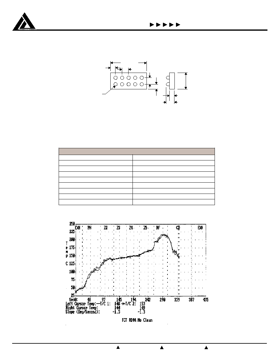
)
A
6
0
1
s
u
l
P
u
C
k
e
t
n
E
(
P
S
O
Typical Solder Reflow Thermal Profile (No Clean Flux)