
© 2003 California Micro Devices Corp. All rights reserved.
09/15/03
430 N. McCarthy Blvd., Milpitas, CA 95035-5112
L Tel: 408.263.3214
L Fax: 408.263.7846 L www.calmicro.com
1
PACSZ1284
IEEE 1284 Parallel Port ESD/EMI/Termination Network
Features
∑
17 EMI filters
∑
17 ESD protectors yielding protection to 30kV
contact discharge, per IEC 61000-4-2 specification
∑
17 terminators with choice of resistor values
∑
28-pin QSOP package
∑
Lead-free version available
Applications
∑
Parallel Ports of PCs, printers, peripherals,
and Set-Top Boxes
Product Description
The PACSZ1284 combines EMI filtering, ESD protec-
tion, and signal termination in a single QSOP package
for parallel port interfaces complying to the IEEE 1284
standard.
The PACSZ1284 provides a complete parallel port ter-
mination solution. It integrates the equivalent of 60 dis-
crete components, making it ideal for space critical
applications. The pins of the device which connect to
the parallel port are protected to 30kV contact dis-
charge, well beyond Level 4 of the IEC 61000-4-2
specification. All other pins are ESD-protected for con-
tact discharges up to 8kV per IEC 61000-4-2.
There are three available values for pull-up resistor R1.
For the PACSZ1284-01, R1 = 1k
; for the PACSZ1284-
02, R1 = 2.2k
; for the PACSZ1284-04, R1 = 4.7k.
P/Active
Æ
technology provides high reliability and low
cost through manufacturing efficiency. the PACSZ1284
is silicon-based and has the same reliability character-
istics as today's integrated circuits.
Electrical Schematic
PACSZ1284-01
R1 = 1k
R2 = 33
C = 150pF
PACSZ1284-02
R1 = 2.2k
R2 = 33
C = 150pF
PACSZ1284-04
R1 = 4.7k
R2 = 33
C = 150pF
C
R1
C
R1
C
R1
C
R1
1
2
28
27
C
R1
3
26
R2
C
R1
4
25
R2
C
R1
5
24
R2
C
R1
6
23
R2
C
R1
7
21
R2
22
C
R1
8
C
R1
9
19
R2
20
C
R1
10
C
R1
11
18
R2
C
R1
12
C
R1
13
17
R2
C
R1
14
16
R2
C
R1
15
© 2003 California Micro Devices Corp. All rights reserved.
2
430 N. McCarthy Blvd., Milpitas, CA 95035-5112
L Tel: 408.263.3214
L Fax: 408.263.7846 L www.calmicro.com
09/15/03
PACSZ1284
Ordering Information
Note 1: Parts are shipped in Tape & Reel form unless otherwise specified.
PIN DESCRIPTIONS
LEADS
NAME
DESCRIPTION
1,2,8,10,
12,15, 27,28
Capacitor-filtered
IEEE 1284 signals which require no series termination.
3-7, 9,11,
13,14
Super I/O Chip side series-termi-
nated
IEEE 1284 signals on the Super I/O Chip side which require
series termination.
16-19, 21,
23-26
Parallel Port
connector side series-terminated
IEEE 1284 signals on the Parallel Port Connector side which
require series termination.
20
V
CC
Supply rail for the device
22
GND
Ground reference for the device
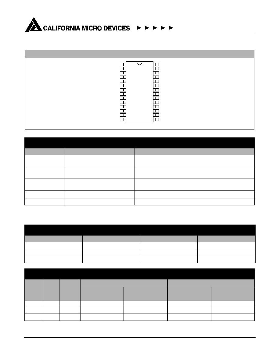
PACKAGE / PINOUT DIAGRAM
Note: This drawing is not to scale.
28-pin QSOP
1
2
3
4
5
6
7
8
20
19
18
17
21
22
9
10
24
23
25
26
11
12
27
28
SUPERCHIP SIDE SERIES-TERMINATED
SUPERCHIP SIDE SERIES-TERMINATED
SUPERCHIP SIDE SERIES-TERMINATED
CAP-FILTERED
SUPERCHIP SIDE SERIES-TERMINATED
CAP-FILTERED
SUPERCHIP SIDE SERIES-TERMINATED
CAP-FILTERED
CAP-FILTERED
CAP-FILTERED
SUPERCHIP SIDE SERIES-TERMINATED
SUPERCHIP SIDE SERIES-TERMINATED
CAP-FILTERED
CONNECTOR SIDE SERIES-TERMINATED
CONNECTOR SIDE SERIES-TERMINATED
CONNECTOR SIDE SERIES-TERMINATED
CONNECTOR SIDE SERIES-TERMINATED
GND
CONNECTOR SIDE SERIES-TERMINATED
V
CC
CONNECTOR SIDE SERIES-TERMINATED
CONNECTOR SIDE SERIES-TERMINATED
CONNECTOR SIDE SERIES-TERMINATED
CAP-FILTERED
13
14
16
15
CONNECTOR SIDE SERIES-TERMINATED
CAP-FILTERED
SUPERCHIP SIDE SERIES-TERMINATED
SUPERCHIP SIDE SERIES-TERMINATED
STANDARD VALUES
RC Code
R1 (
)
R2 (
)
C (pF)
01
1.0k
33
150
02
2.2k
33
150
04
4.7k
33
150
PART NUMBERING INFORMATION
RC
Code
Pins
Package
Standard Finish
Lead-free Finish
Ordering Part
Number
1
Part Marking
Ordering Part
Number
1
Part Marking
01
28
QSOP
PACSZ128401Q
PACSZ128401Q
PACSZ128401QR
PACSZ128401QR
02
28
QSOP
PACSZ128402Q
PACSZ128402Q
PACSZ128402QR
PACSZ128402QR
04
28
QSOP
PACSZ128404Q
PACSZ128404Q
PACSZ128404QR
PACSZ128404QR

© 2003 California Micro Devices Corp. All rights reserved.
09/15/03
430 N. McCarthy Blvd., Milpitas, CA 95035-5112
L Tel: 408.263.3214
L Fax: 408.263.7846
L www.calmicro.com
3
PACSZ1284
Specifications
Note 1: Guaranteed by design and characterization.
Note 2: ESD voltage applied between Input/Connector pins and ground, one pin at a time.
Note 3: Pins 3-7, 9, 11, 13, and 14 typically connect to the I/O pins of a Super I/O chip.
Note 4: Pins 1, 2, 8, 10, 12, 15-19, 21, and 23-28 typically connect to the Parallel Port connector.
ABSOLUTE MAXIMUM RATINGS
PARAMETER
RATING
UNITS
V
CC
Voltage
5.5
V
Input Voltage Range, no clamping
-0.4 to 5.5
V
Storage Temperature Range
-40 to +150
∞C
Power Dissipation per Resistor
0.1
W
Package Power Dissipation
1.0
W
STANDARD OPERATING CONDITIONS
PARAMETER
RATING
UNITS
V
CC
Voltage
5.0
V
Operating Temperature
-40 to +85
∞C
ELECTRICAL OPERATING CHARACTERISTICS
SYMBOL
PARAMETER
CONDITIONS
MIN
TYP
MAX
UNITS
TOL
R
Absolute Resistance Tolerance
Measured at T
A
=25∞C
+20
%
TOL
C
Absolute Capacitance Tolerance
Measured at 1MHz, 2.5VDC, T
A
=25∞C
+20
%
I
LEAK
Leakage current to GND
Measured at 5.0VDC, T
A
=25∞C
1
10
µA
V
ESDi
ESD protection, input pins
Pins 3,4,5,6,7,9,11,13, & 14, per IEC
61000-4-2 specification,
Notes 1,2,3
+8
kV
V
ESD
ESD protection, connector pins
Pins 1,2,8,10,12,15,16,17,18,19,
21,23,24,25,26,27, & 28, per
IEC 61000-4-2 specification
Notes 1,2,4
+30
kV
V
CLAMP
Clamping voltage under ESD
discharge
ESD applied to connector pin, mea-
sured at corresponding input pin;
+8kV discharge, Human Body Model
Notes 1,2
8.3
V
ESD applied to connector pin,
measured at corresponding input pin;
-8kV discharge, Human Body Model;
Notes 1,2
-2.7
V

© 2003 California Micro Devices Corp. All rights reserved.
4
430 N. McCarthy Blvd., Milpitas, CA 95035-5112
L Tel: 408.263.3214
L Fax: 408.263.7846 L www.calmicro.com
09/15/03
PACSZ1284
Performance Information
Filter Capacitors
The IEEE 1284 specification requires both termination
and EMI filtering on a total of 17 lines. Basic filtering is
provided through the presence of a capacitor on all sig-
nal lines. The filter capacitor is the junction capacitance
of an ESD diode. The typical capacitance at a reverse
voltage of 2.5V is 150pF. This diode capacitance is
somewhat voltage dependent. See
Figure 1
.
Figure 1. Diode Capacitance vs. Reverse Voltage
The higher speed Data and Strobe lines (9 in total)
require an additional series resistor termination for
proper operation, while the eight (8) Status lines do
not. See
Table 1 on page 5
.
Filter Insertion Loss
Figure 2
shows the typical Insertion Loss graphs of the
PACSZ1284 for Data and Strobe signals. The curves
are dependent on the physical location of the filter ele-
ments with respect to the ground terminal of this
device. These graphs are measured in a 50
environ-
ment on a Hewlett Packard HP 8753C Analyzer. The
signal source is introduced at the resistor input and the
output is measured at the corresponding protection
diode. The actual pins measured are labeled in the
Figure 2
graph.
Figure 2. Typical Filter Insertion Loss
Frequency (MHz)

© 2003 California Micro Devices Corp. All rights reserved.
09/15/03
430 N. McCarthy Blvd., Milpitas, CA 95035-5112
L Tel: 408.263.3214
L Fax: 408.263.7846
L www.calmicro.com
5
PACSZ1284
Application Information
Termination Considerations
The IEEE 1284 specification requires both termination
and EMI filtering on a total of 17 signal lines. Control
and Status lines (8 in total) only require a pull-up resis-
tor and a filter capacitor. The Data lines and Strobe
also require a series termination resistor in addition to
the pull-up resistors and filter capacitors. See
Table 1
,
in conjunction with the schematic diagram on page 1.
Interfacing to IEEE 1284 Connectors
IEEE 1284 defines three interface connectors:
∑
1284 A is a 25-pin DB series connector which is
the de facto PC standard for the host connection.
∑
1284 B is a 36-pin, 0.085 inch centerline connector
used on the peripheral device.
∑
1284 C is a new 36-pin, 0.050 inch centerline con-
nector which can be used for both host and periph-
eral.
Figure 3A
shows a possible hook-up between the
1284-A connector on a PC motherboard and the
PACSZ1284, illustrating how the pin configuration of
the PACSZ1284 allows for easy interconnect between
the two. The dotted I/O signals of the PACSZ1284 will
typically be connected to a Super I/O chip on the
motherboard.
Figure 3B
shows a possible hook-up between the
1284-B connector on a peripheral and the PACSZ1284.
Figure 3C
shows a possible hook-up between the
1284-C connector and the PACSZ1284.
Figure 3. Example Connections of IEEE 1284 Connectors with PACSZ1284
Table 1: IEEE 1284 Termination Requirements
SIGNAL TERMINATION REQUIREMENTS
Signal Name
Series Termination
Data1 - Data8
Yes
Strobe
Yes
Init
Not Required
AutoFeedXT
Not Required
Selectin
Not Required
ACK
Not Required
Busy
Not Required
Paper Empty
Not Required
Select
Not Required
Fault
Not Required
1
14
1
19
1
1
1
1
2
20
= FLOW
THROUGH
SIGNALS
= GND
= V
CC
SUPER 1284
SUPER 1284
SUPER 1284
1284-A Connector
Host
1284-B Connector
Peripheral
1284-C Connector
Host/Peripheral
25
13
36
18
36
18
19
Figure 3A:
Figure 3B:
Figure 3C:
= GND
= V
CC
PACSZ1284
PACSZ1284
PACSZ1284

© 2003 California Micro Devices Corp. All rights reserved.
6
430 N. McCarthy Blvd., Milpitas, CA 95035-5112
L Tel: 408.263.3214
L Fax: 408.263.7846 L www.calmicro.com
09/15/03
PACSZ1284
Application Information (continued)
Table 2
provides the IEEE 1284 signal assignments for
the three connectors, and example PACSZ1284 pin
connections.
When connecting a 1284-A host to a 1284-B periph-
eral, the "Peripheral Logic High" signal is not used.
Similarly, when a 1284-A host is connected to a 1284-
C peripheral, the "Peripheral Logic High" and "Host
Logic High" are not used. These two signals are
optionally used to detect a "Power Off" or "Cable Dis-
connect" state for host and peripheral, respectively.
Table 2: IEEE 1284 Connector Pinouts and PACSZ1284 Connection Guidelines
PACSZ1284
PIN TYPE
1284-A
25-PIN DSUB
1284-B
36-PIN CHAMP
1284-C
36-PIN HIGH
DENSITY
SIGNAL
PIN
SIGNAL
PIN
SIGNAL
PIN
P-Port conn. side, series-terminated (16-19, 21, or 23-26)
STROBE
1
STROBE
1
STROBE
15
P-Port conn. side, series-terminated (16-19, 21, or 23-26)
Data 1
2
Data 1
2
Data 1
6
P-Port conn. side, series-terminated (16-19, 21, or 23-26)
Data 2
3
Data 2
3
Data 2
7
P-Port conn. side, series-terminated (16-19, 21, or 23-26)
Data 3
4
Data 3
4
Data 3
8
P-Port conn. side, series-terminated (16-19, 21, or 23-26)
Data 4
5
Data 4
5
Data 4
9
P-Port conn. side, series-terminated (16-19, 21, or 23-26)
Data 5
6
Data 5
6
Data 5
10
P-Port conn. side, series-terminated (16-19, 21, or 23-26)
Data 6
7
Data 6
7
Data 6
11
P-Port conn. side, series-terminated (16-19, 21, or 23-26)
Data 7
8
Data 7
8
Data 7
12
P-Port conn. side, series-terminated (16-19, 21, or 23-26)
Data 8
9
Data 8
9
Data 8
13
Capacitor-filtered (1, 2, 8, 10, 12, 15, 27, or 28)
ACK
10
ACK
10
ACK
3
Capacitor-filtered (1, 2, 8, 10, 12, 15, 27, or 28)
BUSY
11
BUSY
11
BUSY
1
Capacitor-filtered (1, 2, 8, 10, 12, 15, 27, or 28)
PError
12
PError
12
PError
5
Capacitor-filtered (1, 2, 8, 10, 12, 15, 27, or 28)
Select
13
Select
13
Select
2
Capacitor-filtered (1, 2, 8, 10, 12, 15, 27, or 28)
AUTOFD
14
AUTOFD
14
AUTOFD
17
Capacitor-filtered (1, 2, 8, 10, 12, 15, 27, or 28)
FAULT
15
FAULT
32
FAULT
4
Capacitor-filtered (1, 2, 8, 10, 12, 15, 27, or 28)
INIT
16
INIT
31
INIT
14
Capacitor-filtered (1, 2, 8, 10, 12, 15, 27, or 28)
Selectin
17
Selectin
36
Selectin
16
Ground
18
Ground
19
Ground
19
Ground
19
Ground
20
Ground
20
Ground
20
Ground
21
Ground
21
Ground
21
Ground
22
Ground
22
Ground
22
Ground
23
Ground
23
Ground
23
Ground
24
Ground
24
Ground
24
Ground
25
Ground
25
Ground
25
Ground
26
Ground
26
Ground
27
Ground
27
Ground
28
Ground
28
Ground
29
Ground
29
Ground
30
Ground
30
Not Defined
33
Ground
31
Not Defined
34
Ground
32
Not Defined
35
Ground
33
Not Defined
15
Ground
34
Logic Ground
16
Ground
35
Chassis GND
17
Not Required
36
Peripheral Logic
18
Host Logic High
18

© 2003 California Micro Devices Corp. All rights reserved.
09/15/03
430 N. McCarthy Blvd., Milpitas, CA 95035-5112
L Tel: 408.263.3214
L Fax: 408.263.7846
L www.calmicro.com
7
PACSZ1284
Mechanical Details
QSOP Mechanical Specifications:
PACSZ1284 devices are packaged in 28-pin QSOP
packages. Dimensions are presented below.
For complete information on the QSOP-28 package,
see the California Micro Devices QSOP Package Infor-
mation document.
* This is an approximate amount which may vary.
Package Dimensions for QSOP-28
PACKAGE DIMENSIONS
Package
QSOP (JEDEC name is SSOP)
Pins
28
Dimensions
Millimeters
Inches
Min
Max
Min
Max
A
1.35
1.75
0.053
0.069
A1
0.10
0.25
0.004
0.010
B
0.20
0.30
0.008
0.012
C
0.18
0.25
0.007
0.010
D
9.80
9.98
0.386
0.393
E
3.81
3.98
0.150
0.157
e
0.64 BSC
0.025 BSC
H
5.79
6.20
0.228
0.244
L
0.40
1.27
0.016
0.050
# per tube
50 pieces*
# per tape
and reel
2500 pieces
Controlling Dimensions: inches
Mechanical Package Diagrams
E
D
H
TOP VIEW
L
END VIEW
C
e
B
A
A1
SEATING
PLANE
SIDE VIEW
5
6
7
8
9
10
11
12
1
2
3
4
24 23
22 21 20
19
18
17
28
27
26
25
Pin 1 Marking
13
14
16
15