©
2004 California Micro Devices Corp. All rights reserved.
09/14/04
430 N. McCarthy Blvd., Milpitas, CA 95035-5112
Tel: 408.263.3214
Fax: 408.263.7846
www.calmicro.com
1
PACUSB-D1/D2/D3
USB Downstream Port Terminator
Features
∑
A low-capacitance USB downstream port termina-
tor, EMI filter, and transient over-voltage (ESD)
protector in a single surface-mounted package
∑
ESD protection to +20kV contact discharge, per
MIL-STD-883D, Method 3015
∑
ESD protection to +15kV contact discharge, per
IEC 61000-4-2 International Standard
∑
Compact SOT23-5 and SC70-5 package options
save board space and lower manufacturing costs
compared to discrete solutions
∑
Capacitors matched to a precision exceeding the
USB specification
∑
Pin-compatible with ST Microelectronics
USBDFxxW5 USB Downstream Port Terminator
∑
Lead-free versions available
Applications
∑
ESD protection and termination of USB
downstream ports
∑
Desktop PCs
∑
Notebooks
∑
Set-top boxes
∑
USB hubs
Product Description
The PACUSB-D1/D2/D3 is a single-channel USB
downstream-port termination network. It integrates
EMI/RFI filter components R1 and C1, as recom-
mended by the USB specification as well as the
required 15k
pull-down resistors (R2) to GND. In
addition, PACUSB-D1/D2/D3 provides a very high
level of protection for sensitive electronic components
that may be subjected to electrostatic discharge (ESD).
The device pins will safely dissipate ESD strikes of
+15kV, exceeding the maximum requirements of the
IEC 61000-4-2 international standard. Using the MIL-
STD-883D (Method 3015) specification for Human
Body Model (HBM) ESD, all pins are protected from
contact discharges to +20kV.
There are three options for the value of the series
resistor R1: 15
, 22, and 33. This series resis-
tance, plus the USB driver output resistance, must be
close to the USB cable's characteristic impedance of
45
(each side) to minimize transmission line reflec-
tions.
The PACUSB-D1/D2/D3 is manufactured in a 5-pin
SC70 or a 5-pin SOT23 package and is available with
optional lead-free finishing.
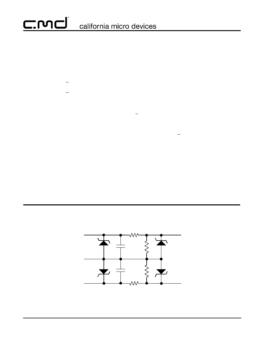
Electrical Schematic
GND
3
4
2
1
C1
C1
R1
R1
R2
R2
5

©
2004 California Micro Devices Corp. All rights reserved.
2
430 N. McCarthy Blvd., Milpitas, CA 95035-5112
Tel: 408.263.3214
Fax: 408.263.7846
www.calmicro.com
09/14/04
PACUSB-D1/D2/D3
Ordering Information
Note 1: Parts are shipped in Tape & Reel form unless otherwise specified.
PIN DESCRIPTIONS
PINS
NAME
DESCRIPTION
1
D+ CNTR
D+ Data to the USB controller circuitry
2
GND
Ground Pin
3
D- CNTR
D- Data to the USB controller circuitry
4
D- CONN
D- Data to the USB connector
5
D+ CONN
D+ Data to the USB connector
PACKAGE / PINOUT DIAGRAMS
Note 1: The "n" shown in part markings above represents either the digit "1," "2," or "3."
5-pin SOT23
D+ CNTR
GND
D- CNTR
D+ CONN
D- CONN
1
2
5
3
4
UD
F
n
/
Top View
5-pin SC70
1
2
5
3
4
DFn /
Top View
Note 2: SOT23 and SC70 package sizes may differ. These drawings are not to scale.
PACUSB-D1Y5/-D2Y5/-D3Y5
PACUSB-D1YB5/-D2YB5/-D3YB5
D+ CNTR
GND
D- CNTR
D+ CONN
D- CONN
DF
nR
Fn
R
-D1Y5R/-D2Y5R/-D3Y5R
-D1YB5R/-D2YB5R/-D3YB5R
PART NUMBERING INFORMATION
Pins
R1 Value
Package
Standard Finish
Lead-free Finish
Ordering Part
Number
1
Part Marking
Ordering Part
Number
1
Part Marking
5
15
SOT23-5
PACUSB-D2Y5
UDF2
PACUSB-D2Y5R
DF2R
22
PACUSB-D3Y5
UDF3
PACUSB-D3Y5R
DF3R
33
PACUSB-D1Y5
UDF1
PACUSB-D1Y5R
DF1R
5
15
SC70-5
PACUSB-D2YB5
DF2
PACUSB-D2YB5R
F2R
22
PACUSB-D3YB5
DF3
PACUSB-D3YB5R
F3R
33
PACUSB-D1YB5
DF1
PACUSB-D1YB5R
F1R

©
2004 California Micro Devices Corp. All rights reserved.
09/14/04
430 N. McCarthy Blvd., Milpitas, CA 95035-5112
Tel: 408.263.3214
Fax: 408.263.7846
www.calmicro.com
3
PACUSB-D1/D2/D3
Specifications
ABSOLUTE MAXIMUM RATINGS
PARAMETER
RATING
UNITS
Storage Temperature Range
-65 to +150
∞C
Power Dissipation per Resistor
100
mW
Package Power Dissipation
200
mW
Voltage on any pin (DC)
6
V
STANDARD OPERATING CONDITIONS
PARAMETER
RATING
UNITS
Operating Temperature
-40 to +85
∞C

©
2004 California Micro Devices Corp. All rights reserved.
4
430 N. McCarthy Blvd., Milpitas, CA 95035-5112
Tel: 408.263.3214
Fax: 408.263.7846
www.calmicro.com
09/14/04
PACUSB-D1/D2/D3
Specifications (cont'd)
Note 1: Electrical operating characteristics guaranteed over standard operating conditions unless specified otherwise.
Note 2: Guaranteed by design and characterization.
Note 3: ESD voltage applied to pins with respect to GND, one at a time; unused pins are left open.
Note 4: Pins 1 and 3 are not connected to the USB port connector, and therefore are not exposed to external ESD hazards. Thus,
they do not require the high ESD protection levels provided for pins 4 and 5.
Note 5: ESD Clamping Voltage is measured at the opposite end of R1 from the pin to which the ESD discharge is applied (e.g., if
ESD is applied to pin 6, then the clamping voltage is measured at pin 1).
ELECTRICAL OPERATING CHARACTERISTICS
(SEE NOTE 1)
SYMBOL PARAMETER
CONDITIONS
MIN
TYP
MAX
UNITS
R1
Resistance of R1 Resistor
(PACUSB-D2Y5/Y5R, -D2YB5/YB5R)
T
A
= 25∞C
12
15
18
R1
Resistance of R1 Resistor
(PACUSB-D3Y5/Y5R, -D3YB5/YB5R)
T
A
= 25∞C
17.6
22
26.4
R1
Resistance of R1 Resistor
(PACUSB-D1Y5/Y5R, -D1YB5/YB5R)
T
A
= 25∞C
26.4
33
39.6
R2
Resistance of R2 Resistor
T
A
= 25∞C
15
k
TCR
Temperature Coefficient of Resistance Note 1
+1300
ppm/
∞C
C1
Capacitance of C1 Capacitor
0 VDC; 30 mVAC; 1MHz; 25∞C
37.6
47
56.4
pF
2.5 VDC; 30 mVAC; 1MHz; 25∞C
25.6
32
38.4
pF
TOL
CM
Matching Tolerance of C1 Capacitors
1MHz; 25∞C
+2
%
I
LEAK
Diode Leakage Current to GND
Measured at 3.3 VDC, 25∞C
1
100
nA
V
RB
Diode Reverse Bias Voltage
I
LOAD
= 10
A; T
A
= 25∞C
5.5
V
V
SIG
Signal Voltage:
Positive Clamp
Negative Clamp
I
LOAD
= 10mA; T
A
= 25∞C
I
LOAD
= 10mA; T
A
= 25∞C
5.6
-0.4
6.8
-0.8
9.0
-1.5
V
V
V
ESD
In-system ESD Withstand Voltage
MIL-STD-883D, Method 3015
(HBM)
IEC 61000-4-2 Contact Discharge
Pins 1, 3; Notes 2,3 and 4
Pins 4, 5; Notes 2 and 3
Pins 4, 5; Notes 2 and 3
+4
+20
+15
kV
kV
kV
V
CL
Clamping voltage under ESD
discharge
MIL-STD-883D, Method 3015
+8kV; Notes 2 and 5
12
V
MIL-STD-883D, Method 3015 -
8kV; Notes 2 and 5
-7
V

©
2004 California Micro Devices Corp. All rights reserved.
09/14/04
430 N. McCarthy Blvd., Milpitas, CA 95035-5112
Tel: 408.263.3214
Fax: 408.263.7846
www.calmicro.com
5
PACUSB-D1/D2/D3
Performance Information
Capacitance vs. Voltage
The C1 capacitance value as a function of DC voltage
across it is presented in
Figure 1
. The curve is normal-
ized to a capacitance of 1.0 capacitance units at 2.5
VDC.
Figure 1. Diode Capacitance vs. DC Voltage (Normalized)
Insertion Loss vs. Frequency Characteristics
Figure 2. Insertion Loss vs. Frequency Performance Curve, PACUSB-D1(SOT23-6)
DC Voltage
No
r
m
a
l
i
z
e
d
C1 Ca
pa
ci
t
a
n
c
e
1.0
1.2
1.4
1.6
0.8
0.6
0.4
0.2
0
0
1
2
3
4
5
6

©
2004 California Micro Devices Corp. All rights reserved.
6
430 N. McCarthy Blvd., Milpitas, CA 95035-5112
Tel: 408.263.3214
Fax: 408.263.7846
www.calmicro.com
09/14/04
PACUSB-D1/D2/D3
Performance Information (cont'd)
Figure 3. Insertion Loss vs. Frequency Performance Curve, PACUSB-D2(SOT23-6)
Figure 4. Insertion Loss vs. Frequency Performance Curve, PACUSB-D3(SOT23-6)

©
2004 California Micro Devices Corp. All rights reserved.
09/14/04
430 N. McCarthy Blvd., Milpitas, CA 95035-5112
Tel: 408.263.3214
Fax: 408.263.7846
www.calmicro.com
7
PACUSB-D1/D2/D3
Application Information
The PACUSB-D1/D2/D3 provides a complete interface
for a single downstream USB port typically found in
computers and USB hubs. It integrates the series
resistors (R1) and the 15k
pull-down resistors (R2)
for both USB data lines (D+ and D-) as well as the
capacitors to ground for EMI suppression. Zener
diodes provide ESD protection up to 15kV contact dis-
charge per the IEC 61000-4-2 standard and protect the
USB controller on both data lines.
The PACUSB-D1/D2/D3 should be placed on the PCB
between the USB controller and the USB connector, as
shown on the Connection Diagram
Figure 5
.
Figure 5. Connection Diagram for PACUSB-D1/D2/D3 Devices
To guarantee the best ESD and filtering performance,
it is recommended to physically locate the PACUSB-
D1/D2/D3 close to the USB connector. Also, the trace
lengths between the PACUSB-D1/D2/D3 and the USB
controller should be kept as short as possible.
DOWN-
USB
USB
CONTROLLER
PACUSB-DnY5/Y5R, -DnYB5/YB5R
C1
C1
R1
R1
R2
R2
D+
D-
D+
D-
STREAM
CONNECTOR
2
1
3
4
5

©
2004 California Micro Devices Corp. All rights reserved.
8
430 N. McCarthy Blvd., Milpitas, CA 95035-5112
Tel: 408.263.3214
Fax: 408.263.7846
www.calmicro.com
09/14/04
PACUSB-D1/D2/D3
Mechanical Details
PACUSB-D1/D2/D3 devices are packaged in SOT23-5
and SC70-5 packages.
SOT23-5 Mechanical Specifications:
Dimensions for PACUSB-D1/D2/D3 devices packaged
in a 5-pin SOT23 package are presented below.
For complete information on the SOT23-5 package,
see the California Micro Devices SOT23 Package
Information document.
* This is an approximate amount which may vary.
Package Dimensions for SOT23-5.
PACKAGE DIMENSIONS
Package
SOT23-5 (JEDEC name is MO-178)
Pins
5
Dimensions
Millimeters
Inches
Min
Max
Min
Max
A
--
1.45
--
0.057
A1
0.00
0.15
0.000
0.006
b
0.30
0.50
0.012
0.020
c
0.08
0.22
0.003
0.009
D
2.75
3.05
0.108
0.120
E
2.60
3.00
0.102
0.118
E1
1.45
1.75
0.057
0.069
e
0.95 BSC
0.0374 BSC
e1
1.90 BSC
0.0748 BSC
L
0.30
0.60
0.0236 0.024
L1
0.60 REF
0.024 REF
# per tape
and reel
3000 pieces*
Controlling dimension: millimeters
Mechanical Package Diagrams
TOP VIEW
5
4
e1
e
E1 E
b
A
SIDE VIEW
D
A1
1
2
3
L1
END VIEW
c
L

©
2004 California Micro Devices Corp. All rights reserved.
09/14/04
430 N. McCarthy Blvd., Milpitas, CA 95035-5112
Tel: 408.263.3214
Fax: 408.263.7846
www.calmicro.com
9
PACUSB-D1/D2/D3
Mechanical Details (continued)
SC70-5 Mechanical Specifications:
Dimensions for PACUSB-D1/D2/D3 devices packaged
in a 5-pin SC70 package are presented below.
For complete information on the SC70-5 package, see
the California Micro Devices SC70 Package Informa-
tion document.
* This is an approximate amount which may vary.
Package Dimensions for SC70-5.
PACKAGE DIMENSIONS
Package
SC70-5
(JEDEC name is MO-203 Issue A)
Pins
5
Dimensions
Millimeters
Min
Max
A
0.80
1.10
A1
0.00
0.10
A2
0.70
1.00
B
0.15
0.30
c
0.08
0.25
D
1.85
2.25
E
1.15
1.35
e
0.65 BSC
HE
2.00
2.40
L
0.26
0.46
# / bag
1000 pieces*
# / tape and reel
3000 pieces*
Mechanical Package Diagrams
TOP VIEW
e
e
E HE
B
A
SIDE VIEW
L
END VIEW
D
A2
A1
c
1
2
3
5
4