
© 2004 California Micro Devices Corp. All rights reserved.
01/28/04
430 N. McCarthy Blvd., Milpitas, CA 95035-5112
L Tel: 408.263.3214
L Fax: 408.263.7846 L www.calmicro.com
1
PACVGA105
VGA Port Companion Circuit
Features
∑
7 channels of ESD protection designed to
meet IEC-1000-4-2 Level-4 ESD requirements
(8kV contact discharge)
∑
Very low loading capacitance from ESD protection
diodes at less than 5pF typical
∑
TTL to CMOS level-translating buffers for the
HSYNC and VSYNC lines
∑
Three independent supply pins (V
CC
, V
RGB
and
V
AUX
) to facilitate operation with sub-micron
Graphics Controller ICs
∑
High impedance pull-ups (50k
nominal to V
AUX
)
for HSYNC and VSYNC inputs
∑
Pull-up resistors (1.8k
nominal to V
CC
) for
DDC_CLK and DDC_DATA lines
∑
Compact 16-pin QSOP package
∑
Lead-free version available
Applications
∑
ESD protection and termination resistors for VGA
(video) port interfaces
∑
Desktop PCs
∑
Notebook computers
∑
LCD monitors
Product Description
The PACVGA105 incorporates 7 channels of ESD pro-
tection for signal lines commonly found in a VGA port
for PCs. ESD protection is implemented with current
steering diodes designed to safely handle the high
peak surge currents associated with the IEC-1000-4-2
Level-4 ESD Protection Standard (8kV contact dis-
charge). When the channels are subjected to an elec-
trostatic discharge, the ESD current pulse is diverted
via the protection diodes into the positive supply rails or
ground where they may be safely dissipated.
The upper ESD diodes for the R, G and B channels are
connected to a separate supply rail (V
RGB
) to facilitate
interfacing to graphics controller ICs with low voltage
supplies. The remaining channels are connected to the
main 5V rail (V
CC
). The lower diodes for the R, G and B
channels are also connected to a dedicated ground pin
(GNDA) to minimize crosstalk due to common ground
impedance.
Two non-inverting buffers are also included in this IC
for buffering the HSYNC and VSYNC signals from the
graphics controller IC. These buffers will accept TTL
input levels and convert them to CMOS output levels
that swing between GND and V
CC
. These drivers have
a nominal 60
output impedance to match the charac-
teristic impedance of the HSYNC and VSYNC lines of
the video cables typically used. The inputs of these
drivers also have high impedance pull-ups (50k
nom.)
pulling up to the V
AUX
rail. In addition, the
DDC_CLOCK and DDC_DATA channels have 1.8k
resistors pulling these inputs up to the main 5V (V
CC
)
rail.
Simplified Electrical Schematic
R
G
B
V
RGB
GNDA
VSYNC_OUT
GNDD
V
CC
1.8k
1.8k
50k
50k
V
AUX
HSYNC_OUT
VSYNC
HSYNC
DDC_DATA
DDC_CLK
© 2004 California Micro Devices Corp. All rights reserved.
2
430 N. McCarthy Blvd., Milpitas, CA 95035-5112
L Tel: 408.263.3214
L Fax: 408.263.7846 L www.calmicro.com
01/28/04
PACVGA105
PIN DESCRIPTIONS
LEAD(s)
NAME
DESCRIPTION
1
HSYNC_OUT
Horizontal sync signal buffer output. Connects to the video connector side of the horizontal sync
line.
2
HSYNC
Horizontal sync signal buffer input. Connects to the VGA Controller side of the horizontal sync
line.
3, 11
GNDD
Digital ground reference supply pin.
4
V
RGB
V
RGB
supply pin. This is an isolated supply pin for the R, G and B ESD protection circuits.
5
B
Blue signal video protection channel. This pin is typically tied to the B video line between the
VGA controller device and the video connector.
6
G
Green signal video protection channel. This pin is typically tied to the G video line between the
VGA controller device and the video connector.
7
R
Red signal video protection channel. This pin is typically tied to the R video line between the
VGA controller device and the video connector.
8
GNDA
Analog ground reference supply pin.
9, 16
V
CC
V
CC
supply pin. This is the main supply input for the DDC_CLK and DDC_DATA pullup resistors
and ESD protection circuits. It is also connected to the sync buffers and to the ESD protection
diodes present on the HSYNC_OUT and VSYNC_OUT lines.
10
DDC_DATA
DDC data pin.
12
DDC_CLK
DDC clock pin.
13
V
AUX
V
AUX
supply pin. This is the supply input for the 50k
pullups connected to the HSYNC and
VSYNC buffer inputs.
14
VSYNC
Vertical sync signal buffer input. Connects to the VGA Controller side of the vertical sync line.
15
VSYNC_OUT
Vertical sync signal buffer output. Connects to the video connector side of the vertical sync line.
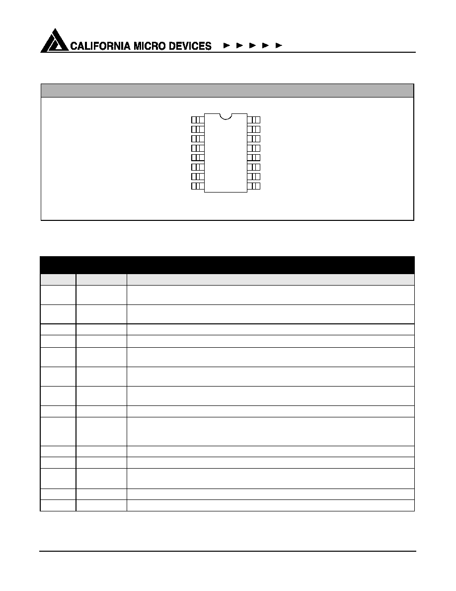
PACKAGE / PINOUT DIAGRAM
Note: This drawing is not to scale.
Top View
16 Pin QSOP
1
2
3
4
14
13
12
11
5
6
7
10
9
8
15
16
V
CC
VSYNC_OUT
VSYNC
V
AUX
DDC_CLK
GNDD
DDC_DATA
HSYNC_OUT
HSYNC
GNDD
V
RGB
B
G
R
V
CC
GNDA
© 2004 California Micro Devices Corp. All rights reserved.
01/28/04
430 N. McCarthy Blvd., Milpitas, CA 95035-5112
L Tel: 408.263.3214
L Fax: 408.263.7846
L www.calmicro.com
3
PACVGA105
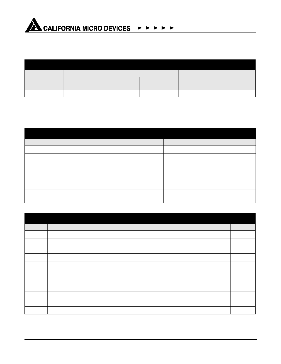
Ordering Information
Note 1: Parts are shipped in Tape & Reel form unless otherwise specified.
Specifications
Note 1: These parameters apply only to the HSYNC and VSYNC signals.
PART NUMBERING INFORMATION
Pins
Package
Standard Finish
Lead-free Finish
Ordering Part
Number
1
Part Marking
Ordering Part
Number
1
Part Marking
16
QSOP
PACVGA105Q
PACVGA105Q
PACVGA105QR
PACVGA105QR
ABSOLUTE MAXIMUM RATINGS
PARAMETER
RATING
UNITS
V
CC
,V
RGB
,V
AUX
Supply Voltage Inputs
[GND - 0.5] to +6.0
V
Diode Forward Current (one diode conducting at a time)
20
mA
DC Voltage at Inputs
R, G, B
HSYNC, VSYNC
DDC_CLK, DDC_DATA
[GND - 0.5] to [V
RGB
+ 0.5]
[GND - 0.5] to [V
AUX
+ 0.5]
[GND - 0.5] to [V
CC
+ 0.5]
V
V
V
Operating Temperature Range
0 to +70
∞C
Storage Temperature Range
-40 to +150
∞C
Package Power Rating
750
mW
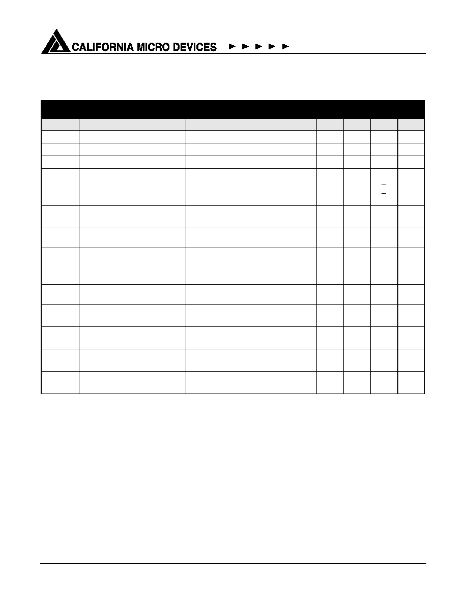
STANDARD OPERATING CONDITIONS
SYMBOL
PARAMETER
MIN
MAX
UNITS
V
CC
Main Supply Voltage
4.5
5.5
V
V
RGB
RGB Supply Voltage
1.7
3.7
V
V
AUX
Auxiliary Supply Voltage
2.9
3.7
V
V
IH
Logic High Input Voltage (Note 1)
2.0
V
V
IL
Logic Low Input Voltage (Note 1)
0.8
V
V
I
Input Voltage
RGB
HSYNC, VSYNC
DDC_CLK, DDC_DATA
0
0
0
V
RGB
V
AUX
V
CC
V
V
V
I
OH
High Level Output Current (Note 1)
-8
mA
I
OL
Low Level Output Current (Note 1)
8
mA
T
A
Free-air Operating Temperature
0
+70
∞C
© 2004 California Micro Devices Corp. All rights reserved.
4
430 N. McCarthy Blvd., Milpitas, CA 95035-5112
L Tel: 408.263.3214
L Fax: 408.263.7846 L www.calmicro.com
01/28/04
PACVGA105
Specifications (cont'd)
Note 1: All parameters specified over standard operating conditions unless otherwise noted.
Note 2: Measured at 1MHz. R/G/B inputs biased at 1.65V with V
RGB
= 3.3V. DDC_CLK and DDC_DATA biased at 2.5V with
V
CC
=5V. HSYNC and VSYNC inputs biased at V
AUX
or GND with V
AUX
= 3.3V and V
CC
= 5V. These parameters are guaran-
teed by design and characterization
Note 3: Per the IEC-61000-4-2 International ESD Standard, Level 4 contact discharge method. V
RGB
and V
CC
must be bypassed to
GND via a low impedance ground plane with a 0.2uF, low inductance, chip ceramic capacitor at each supply pin. ESD pulse
is applied between the applicable pins and GND. ESD pulse can be positive or negative with respect to GND. Applicable
pins are: R, G, B, HSYNC_OUT, VSYNC_OUT, DDC_CLK and DDC_DATA. The HSYNC and VSYNC inputs are ESD pro-
tected to the industry standard 2kV per the Human Body Model (MIL-STD-883, Method 3015).
Note 4: Applicable to the SYNC buffers only. Input signals swing between 0V and 3.0V, with rise and fall times
5ns. Guaranteed by
correlation to buffer output drive currents.
ELECTRICAL OPERATING CHARACTERISTICS
(SEE NOTE 1)
SYMBOL
PARAMETER
CONDITIONS
MIN
TYP
MAX
UNITS
V
F
Diode Forward Voltage
I
F
= 10mA
1.0
V
V
OH
Logic High Output Voltage
I
OH
= -4mA, V
CC
= 4.5V
4.0
V
V
OL
Logic Low Output Voltage
I
OL
= 4mA, V
CC
= 4.5V
0.4
V
I
IN
Input Current
R, G and B pins
HSYNC, VSYNC pins
HSYNC, VSYNC pins
V
RGB
= 3.63V, V
IN
= V
RGB
or GND
V
AUX
= 3.63V, V
IN
= V
AUX
V
AUX
= 3.63V, V
IN
= GND
-30
-72.5
+1
+1
-95
µA
µA
µA
I
CC
V
CC
Supply Current
V
CC
= 5.5V; V
AUX
= V
RGB
= 2.97V; All
inputs and outputs floating
35
100
µA
I
RGB
V
RGB
Supply Current
R, G and B pins at V
CC
or GND; All
inputs and outputs floating
10
µA
C
IN
Input Capacitance
R, G and B pins
HSYNC, VSYNC pins
DDC_DATA, DDC_CLK pins
Note 2 applies for all cases
5
10
5
pF
pF
pF
R
PU
Pull-up Resistance
DDC_DATA, DDC_CLK pins
1.62
1.8
1.98
k
V
ESD
ESD Withstand Voltage
V
CC
= 5V; V
RGB
= 3.3V;
V
AUX
= 3.3V; Note 3
±8
kV
t
PLH
SYNC Buffer L => H
Propagation Delay
C
L
= 50pF; V
CC
= 5.0V;
R
L
= 500
; Note 4
7.0
15.0
ns
t
PHL
SYNC Buffer H => L
Propagation Delay
C
L
= 50pF; V
CC
= 5.0V;
R
L
= 500
; Note 4
7.0
15.0
ns
t
R,
t
F
SYNC Buffer Output Rise & Fall
Times
C
L
= 50pF; V
CC
= 5.0V;
R
L
= 500
; Note 4
7.0
ns

© 2004 California Micro Devices Corp. All rights reserved.
01/28/04
430 N. McCarthy Blvd., Milpitas, CA 95035-5112
L Tel: 408.263.3214
L Fax: 408.263.7846
L www.calmicro.com
5
PACVGA105
Application Information
Figure 1. Typical Connection Diagram
GNDA, the negative voltage rail for the R, G and B diodes is not connected internally to GNDD. GNDA should ide-
ally be connected to the ground of the video DAC IC. This will prevent any ground bounce caused by digital signals
from injecting noise onto the R, G and B signals. Analog GND and digital GND are typically connected on the
printed circuit board.
Red
2
14
10
12
9,16
4
V
i
deo Conne
c
t
or
V
i
d
eo Co
nt
rol
l
er
H-Sync
V-Sync
DDC_Data
DDC_Clk
Blue
Grn
H-Sync
V-Sync
DDC_Data
DDC_Clk
Red
Green
Blue
PACVGA105
DDC_DATA
DDC_CLK
HSYNC
VSYNC
7
R
G
B
6
5
VF
**
VF
**
VF
**
V
RGB
GNDA
GNDD
HSYNC_OUT
VSYNC_OUT
15
1
To Video
13
V
CC
V
AUX
0.2uF
0.2uF
SF
**
SF
**
3, 11
8
VF** - VIDEO EMI Filter
SF** - SYNC EMI Filter
5V
3.3V
ANALOG
GND
DIGITAL
GND
DAC V
DD

© 2004 California Micro Devices Corp. All rights reserved.
6
430 N. McCarthy Blvd., Milpitas, CA 95035-5112
L Tel: 408.263.3214
L Fax: 408.263.7846 L www.calmicro.com
01/28/04
PACVGA105
Mechanical Details
QSOP Mechanical Specifications
PACVGA105 devices are packaged in 16-pin QSOP
packages. Dimensions are presented below.
For complete information on the QSOP-16 package,
see the California Micro Devices QSOP Package Infor-
mation document.
* This is an approximate number which may vary.
Package Dimensions for QSOP-16
PACKAGE DIMENSIONS
Package
QSOP (JEDEC name is SSOP)
Pins
16
Dimensions
Millimeters
Inches
Min
Max
Min
Max
A
1.35
1.75
0.053
0.069
A1
0.10
0.25
0.004
0.010
B
0.20
0.30
0.008
0.012
C
0.18
0.25
0.007
0.010
D
4.80
5.00
0.189
0.197
E
3.81
3.98
0.150
0.157
e
0.64 BSC
0.025 BSC
H
5.79
6.19
0.228
0.244
L
0.40
1.27
0.016
0.050
# per tube
100 pcs*
# per tape
and reel
2500 pcs
Controlling dimension: inches
Mechanical Package Diagrams
E
D
H
TOP VIEW
L
END VIEW
C
e
B
A
A1
SEATING
PLANE
SIDE VIEW
5
6
7
8
1
2
3
4
12
11
10
9
16
15
14
13
Pin 1 Marking