© 2000 California Micro Devices Corp. All rights reserved.
4/00
215 Topaz Street, Milpitas, California 95035 Tel: (408) 263-3214 Fax: (408) 263-7846 www.calmicro.com
1
CALIFORNIA MICRO DEVICES
PACVGA201
VGA PORT COMPANION CIRCUIT
Features
7 channels of ESD protection for all VGA port
connector pins meeting IEC-61000-4-2 Level-4 ESD
requirements (8KV contact discharge)
Very low loading capacitance from ESD protection
diodes on VIDEO lines, 4pF typical
TTL to CMOS level-translating buffers with power
down mode for HSYNC and VSYNC lines
Three power supplies for design flexibility
Compact 16-pin QSOP package
C0651299
PAC VGA201 is a trademark of California Micro Devices Corp.
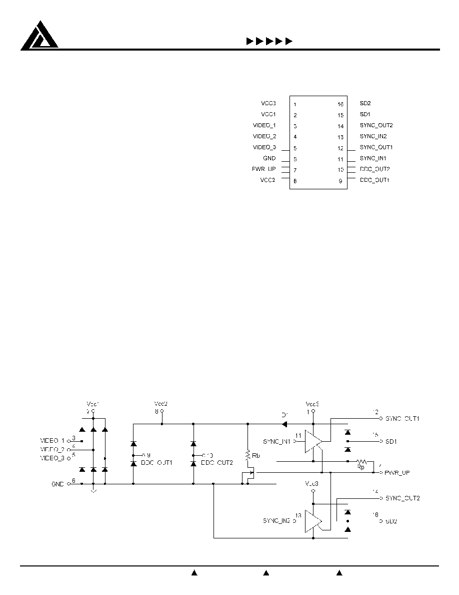
Pin Diagram
Schematic Diagram
Product Description
The PACVGA201 incorporates 7 channels of ESD protection for all signal lines commonly found in a VGA port. ESD protection
is implemented with current steering diodes designed to safely handle the high surge currents encountered with IEC-61000-4-
2 Level-4 ESD Protection (8KV contact discharge). When a channel is subjected to an electrostatic discharge, the ESD current
pulse is diverted via the protection diodes into the positive supply rail or ground where it may be safely dissipated.
Separate positive supply rails are provided for the VIDEO, DDC_OUT and SYNC channels to facilitate interfacing with low
voltage video controller ICs and provide design flexibility in multiple-supply-voltage environments.
An internal diode (D1, in schematic below) is provided such that V
CC2
is derived from V
CC3
. (V
CC2
does not require an external
power supply input.) In applications where V
CC3
may be powered down, diode D1 blocks any DC current path from the
DDC_OUT pins back to the powered down V
CC3
rail via the upper ESD protection diodes.
Two non-inverting drivers provide buffering for the HSYNC and VSYNC signals from the Video Controller IC (SYNC1, SYNC2).
These buffers accept TTL input levels and convert them to CMOS output levels that swing between Ground and V
CC3
.
When the PWR_UP input is driven LOW the SYNC inputs can be floated without causing the SYNC buffers to draw any current
from the V
CC3
supply. When the PWR_UP input is LOW the SYNC outputs are driven LOW.
16-PIN QSOP PACKAGE
©2000 California Micro Devices Corp. All rights reserved.
4/00
215 Topaz Street, Milpitas, California 95035 Tel: (408) 263-3214 Fax: (408) 263-7846 www.calmicro.com
2
CALIFORNIA MICRO DEVICES
PACVGA201
S
G
N
I
T
A
R
M
U
M
I
X
A
M
E
T
U
L
O
S
B
A
r
e
t
e
m
a
r
a
P
g
n
i
t
a
R
t
i
n
U
V
1
C
C
V
,
3
C
C
e
g
a
tl
o
v
y
l
p
p
u
s
0
.
6
+
,
5
.
0
-
D
N
G
V
:
s
t
u
p
n
i
t
a
e
g
a
tl
o
v
C
D
V
3
_
O
E
D
I
V
,
2
_
O
E
D
I
V
,
1
_
O
E
D
I
V
V
,
5
.
0
-
D
N
G
1
C
C
5
.
0
+
V
2
T
U
O
_
C
D
D
,
1
T
U
O
_
C
D
D
V
,
5
.
0
-
D
N
G
2
C
C
5
.
0
+
V
2
N
I
_
C
N
Y
S
,
1
N
I
_
C
N
Y
S
V
,
5
.
0
-
D
N
G
3
C
C
5
.
0
+
V
:
e
r
u
t
a
r
e
p
m
e
T
e
g
a
r
o
t
S
0
5
1
+
o
t
0
4
-
o
C
t
n
e
i
b
m
A
g
n
it
a
r
e
p
O
0
7
+
o
t
0
o
C
n
o
it
a
p
is
si
d
r
e
w
o
p
e
g
a
k
c
a
P
5
7
.
0
W
S
C
I
T
S
I
R
E
T
C
A
R
A
H
C
G
N
I
T
A
R
E
P
O
L
A
C
I
R
T
C
E
L
E
)
e
s
i
w
r
e
h
t
o
d
e
i
f
i
c
e
p
s
s
s
e
l
n
u
s
n
o
i
t
i
d
n
o
c
g
n
i
t
a
r
e
p
o
r
e
v
o
(
l
o
b
m
y
S
r
e
t
e
m
a
r
a
P
s
n
o
i
t
i
d
n
o
C
N
I
M
P
Y
T
X
A
M
T
I
N
U
I
1
C
C
V
1
C
C
t
n
e
r
r
u
c
y
l
p
p
u
s
V
1
C
C
V
5
=
0
1
A
u
I
3
C
C
V
3
C
C
t
n
e
rr
u
c
y
l
p
p
u
s
V
3
C
C
V
r
o
D
N
G
t
a
s
t
u
p
n
i
C
N
Y
S
;
V
5
=
3
C
C
;
0
1
A
u
V
t
a
n
i
p
P
U
_
R
W
P
;
3
C
C
d
e
d
a
o
l
n
u
s
t
u
p
t
u
o
C
N
Y
S
V
3
C
C
P
U
_
R
W
P
;
V
0
.
3
t
a
s
t
u
p
n
i
C
N
Y
S
;
V
5
=
0
0
2
A
u
V
t
a
n
i
p
3
C
C
d
e
d
a
o
l
n
u
s
t
u
p
t
u
o
C
N
Y
S
;
V
3
C
C
C
N
Y
S
;
D
N
G
t
a
t
u
p
n
i
P
U
_
R
W
P
;
V
5
=
0
1
A
u
d
e
d
a
o
l
n
u
s
t
u
p
t
u
o
V
2
C
C
V
2
C
C
e
g
a
tl
o
v
ti
u
c
ri
c
n
e
p
o
n
i
p
V
2
C
C
V
m
o
rf
d
e
v
ir
e
d
y
ll
a
n
r
e
t
n
i
e
g
a
tl
o
v
3
C
C
a
i
v
V
3
C
C
8
.
0
-
V
;
n
w
a
r
d
t
n
e
r
r
u
c
l
a
n
r
e
t
x
e
o
n
;
1
D
e
d
o
i
d
V
H
I
e
g
a
tl
o
v
t
u
p
n
i
h
g
i
H
c
i
g
o
L
1
V
3
C
C
V
0
.
5
=
0
.
2
V
V
L
I
e
g
a
tl
o
v
t
u
p
n
i
w
o
L
c
i
g
o
L
1
V
3
C
C
V
0
.
5
=
8
.
0
V
V
H
O
e
g
a
tl
o
v
t
u
p
t
u
o
h
g
i
H
c
i
g
o
L
2
I
H
O
V
,
A
m
4
-
=
3
C
C
V
0
.
5
=
4
.
4
V
V
L
O
e
g
a
tl
o
v
t
u
p
t
u
o
w
o
L
c
i
g
o
L
2
I
L
O
V
,
A
m
4
=
3
C
C
V
0
.
5
=
4
.
0
V
R
b
R
,
p
e
u
l
a
v
r
o
t
s
i
s
e
R
V
,
P
U
_
R
W
P
3
C
C
V
0
.
5
=
5
.
0
1
2
M
I
N
t
n
e
rr
u
c
t
u
p
n
I
s
t
u
p
n
i
O
E
D
I
V
V
1
C
C
V
;
V
5
=
N
I
V
=
1
C
C
D
N
G
r
o
1
±
µA
s
t
u
p
n
i
C
N
Y
S
V
,
C
N
Y
S
H
V
3
C
C
V
;
V
5
=
N
I
V
=
3
C
C
D
N
G
r
o
1
±
µA
C
N
I
e
c
n
a
ti
c
a
p
a
c
t
u
p
n
I
4
3
_
O
E
D
I
V
,
2
_
O
E
D
I
V
,
1
_
O
E
D
I
V
V
1
C
C
V
;
V
0
.
5
=
N
I
z
H
M
1
t
a
d
e
r
u
s
a
e
m
;
V
5
.
2
=
0
.
4
F
p
V
1
C
C
V
;
V
5
.
2
=
N
I
z
H
M
1
t
a
d
e
r
u
s
a
e
m
;
V
5
2
.
1
=
5
.
4
t
H
L
P
y
a
l
e
d
n
o
it
a
g
a
p
o
r
p
H
-
L
s
r
e
v
ir
d
C
N
Y
S
C
L
V
;
F
p
0
5
=
3
C
C
t
t
u
p
n
I
;
V
5
=
r
t
d
n
a
f
<
s
n
5
8
2
1
s
n
t
L
H
P
y
a
l
e
d
n
o
it
a
g
a
p
o
r
p
L
-
H
s
r
e
v
ir
d
C
N
Y
S
C
L
V
;
F
p
0
5
=
3
C
C
t
t
u
p
n
I
;
V
5
=
r
t
d
n
a
f
<
s
n
5
8
2
1
s
n
t
r
t
,
f
s
e
m
it
ll
a
f
&
e
si
r
t
u
p
t
u
o
s
r
e
v
ir
d
C
N
Y
S
C
L
V
;
F
p
0
5
=
3
C
C
t
t
u
p
n
I
;
V
5
=
r
t
d
n
a
f
<
s
n
5
7
s
n
V
D
S
E
e
g
a
tl
o
v
d
n
a
t
s
h
ti
w
D
S
E
4
,
3
V
1
C
C
V
=
2
C
C
V
=
3
C
C
V
5
=
8
±
V
k
Note 1: These parameters apply only to SYNC_IN1, SYNC_IN2 and PWR_UP.
Note 2: These parameters apply only to SYNC_OUT1 and SYNC_OUT2.
Note 3: Per the IEC-61000-4-2 International ESD Standard, Level 4 contact discharge method. V
CC1
, V
CC2
and V
CC3
must be bypassed to GND via
a low impedance ground plane with a 0.2uF or greater, low inductance, chip ceramic capacitor at each supply pin. ESD pulse is applied
between the applicable pins and GND. ESD pulse can be positive or negative with respect to GND. Applicable pins are: VIDEO_1,
VIDEO_2, VIDEO_3, SYNC_OUT1, SD1, SYNC_OUT2, SD2, DDC_OUT1 and DDC_OUT2. All other pins are ESD protected to the
industry standard 2kV per the Human Body model (MIL-STD-883, Method 3015).
Note 4: This parameter is guaranteed by design and characterization.

© 2000 California Micro Devices Corp. All rights reserved.
4/00
215 Topaz Street, Milpitas, California 95035 Tel: (408) 263-3214 Fax: (408) 263-7846 www.calmicro.com
3
CALIFORNIA MICRO DEVICES
PACVGA201
Typical Connection Diagram
A resistor may be necessary between the V
CC2
pin and ground if protection against a stream of ESD pulses is required
while the PACVGA201 is in the power-down state. The value of this resistor should be chosen such that the extra
charge deposited into the V
CC2
bypass capacitor by each ESD pulse will be discharged before the next ESD pulse occurs.
The maximum ESD repetition rate specified by the IEC-61000-4-2 standard is one pulse per second. When the PACVGA201
is in the power-up state, an internal discharge resistor is connected to ground via a FET switch for this purpose.
For the same reason, V
CC1
and V
CC3
may also require bypass capacitor discharging resistors to ground if there are no
other components in the system to provide a discharge path to ground.
When placing an order please specify desired shipping: Tubes or Tape & Reel.
T
S
R
A
D
N
A
N
O
I
T
A
M
R
O
F
N
I
G
N
I
R
E
D
R
O
T
R
A
P
D
e
g
a
k
c
a
P
r
e
b
m
u
N
t
r
a
P
g
n
i
r
e
d
r
O
s
n
i
P
e
l
y
t
S
g
n
i
k
r
a
M
t
r
a
P
6
1
P
O
S
Q
Q
1
0
2
A
G
V
C
A
P