 | –≠–ª–µ–∫—Ç—Ä–æ–Ω–Ω—ã–π –∫–æ–º–ø–æ–Ω–µ–Ω—Ç: CLM2950AC | –°–∫–∞—á–∞—Ç—å:  PDF PDF  ZIP ZIP |

150mA Low Dropout
Voltage Regulators
CLM2950 / CLM2951
FEATURES
∑
∑
5V, 3.3V, and 3.0V Versions at 150mA Output
∑
∑
Very Low Quiescent Current
∑
∑
Low Dropout Voltage
∑
∑
Extremely Tight Load and Line Regulation
∑
∑
Very Low Temperature Coefficient
∑
∑
Needs Only 1
µ
F for Stability
∑
∑
Current and Thermal Limiting
∑
∑
Unregulated DC Input can Withstand -20V Reverse
Battery and +60V Positive Transients
∑
∑
Similar Replacement for LP2950/LP2951 Sockets
CLM2951 Versions Only
∑
∑
Error Flag Warns of Output Dropout
∑
∑
Logic-Controlled Electronic Shutdown
∑
∑
Output Programmable from 1.24 to 29V
APPLICATIONS
∑
∑
Battery Powered Systems
∑
∑
Cordless Telephones
∑
∑
Radio Control Systems
∑
∑
Portable / Palm Top / Notebook Computers
∑
∑
Portable Consumer Equipment
∑
∑
Portable Instrumentation
∑
∑
Avionics
∑
∑
Automotive Electronics
∑
∑
SMPS Post-Regulator
∑
∑
Voltage Reference
PRODUCT DESCRIPTION
Calogic's CLM2950 and CLM2951 are low power voltage
regulators. These devices are an excellent choice for use in
battery-powered applications such as cordless telephones,
radio control systems, and portable computers. The CLM2950
and CLM2951 features very low quiescent current and very
low dropout voltage (Typ. 50mV at light load and 380mV at
100mA). This includes a tight initial tolerance of 0.5% typ.,
extremely good load and line regulation of 0.05% typ. and
very low output temperature coefficient, making the
CLM2950/CLM2951 useful as a low-power voltage reference.
Other key additional features of this device includes higher
output current (150mA), positive transient protection up to 60V
(Load dump), and the ability to survive an unregulated input
voltage transient of -20V below ground (reverse battery).
The error flag output feature is used as power-on reset for
warning of a low output voltage, due to falling voltage input of
batteries. Another feature is the logic-compatible shutdown
input which enables the regulator to be switched on and off.
The CLM2950 is offered in a 3-pin TO-92 package compatible
with other 5 volt regulators. The CLM2951 is also available in
8-pin plastic and SO-8.
The regulator output voltage may be pin-strapped for a 5V,
3.3V and 3.0 volts or programmed from 1.24 volt to 29 volts
with an external pair of resistors.
ORDERING INFORMATION
PART
PACKAGE
TEMPERATURE RANGE
CLM2950ACN-X
TO-92 (3-Pin)
IND.
CLM2950CN-X
TO-92 (3-Pin)
IND.
CLM2951ACP-X
Plastic DIP (8-Pin)
IND.
CLM2951CP-X
Plastic DIP (8-Pin)
IND.
CLM2951ACS-X
Plastic SOIC (8-Pin)
IND.
CLM2951CS-X
Plastic SOIC (8-Pin)
IND.
X = 3.0V, 3.3V or 5.0V
CORPORATION
PIN CONNECTIONS
1D-47
1
2
3
1. OUTPUT
2. GROUND
3. INPUT
TO-92
BOTTOM VIEW
GROUND
1
2
3
8
7
6
4
5
ERROR
CLM2951
1D-46
8-PIN SURFACE MOUNT
5V OR 3.3V TAP
FEEDBACK
INPUT
SHUTDOWN
SENSE
OUTPUT
TOP VIEW
CALOGIC CORPORATION, 237 Whitney Place, Fremont, California 94539, Telephone: 510-656-2900, FAX: 510-651-3025
ABSOLUTE MAXIMUM RATINGS
Power Dissipation . . . . . . . . . . . . . . . . . . . . . Internally Limited
Lead Temp. (Soldering, 5 Seconds) . . . . . . . . . . . . . . . 260
o
C
Storage Temperature Range . . . . . . . . . . . . . . . -65 to +150
o
C
Operating Junction Temperature Range
CLM2951 . . . . . . . . . . . . . . . . . . . . . . . . . . . . -55 to +150
o
C
CLM2950AC/CLM2950C
CLM2951AC/CLM2951C . . . . . . . . . . . . . . . . -40 to +125
o
C
Input Supply Voltage . . . . . . . . . . . . . . . . . . . . . . . -20 to +60V
Feedback Input Voltage . . . . . . . . . . . . . . . . . . . . -1.5 to +30V
Shutdown Input Voltage. . . . . . . . . . . . . . . . . . . . -0.3 to +30V
Error Comparator Output . . . . . . . . . . . . . . . . . . . -0.3 to +30V
ESD Rating . . . . . . . . . . . . . . . . . . . . . . . . . . . . . . . . 2KV Min
CLM2950 / CLM2951
CORPORATION
CALOGIC CORPORATION, 237 Whitney Place, Fremont, California 94539, Telephone: 510-656-2900, FAX: 510-651-3025
ELECTRICAL CHARACTERISTICS: V
S
= 15V, T
A
= 25
o
C, unless otherwise specified.
PARAMETER
CLM2951
CLM2950AC
CLM2951AC
CLM2950C
CLM2951C
UNITS
CONDITIONS
(Note 2)
MIN
TYP
MAX
MIN
TYP
MAX
MIN
TYP
MAX
3V VERSIONS
Output Voltage
2.985
2.964
3.0
3.015
3.036
2.985
2.970
2.964
3.0
3.0
3.0
3.015
3.030
3.036
2.970
2.955
2.940
3.0
3.0
3.0
3.030
3.045
3.060
V
V
V
T
J
= 25
o
C
-25
o
C
T
J
85
o
C
Full Operating Temperature
Output Voltage
2.955
3.0
3.045
2.958
3.0
3.042
2.928
3.0
3.072
V
100
µ
A
I
L
150mA,T
J
T
JMAX
3.3V VERSIONS
Output Voltage
3.284
3.260
3.3
3.317
3.340
3.284
3.267
3.260
3.3
3.3
3.3
3.317
3.333
3.340
3.267
3.251
3.234
3.3
3.3
3.3
3.333
3.350
3.366
V
V
V
T
J
= 25
o
C
-25
o
C
T
J
85
o
C
Full Operating Temperature
Output Voltage
3.251
3.3
3.350
3.254
3.3
3.346
3.221
3.3
3.379
V
100
µ
A
I
L
150mA, T
J
T
JMAX
5V VERSIONS
Output Voltage
4.975
4.94
5.0
5.025
5.06
4.975
4.95
4.94
5.0
5.0
5.0
5.025
5.050
5.06
4.95
4.925
4.90
5.0
5.0
5.0
5.05
5.075
5.10
V
V
V
T
J
= 25
o
C
-25
o
C
T
J
85
o
C
Full Operating Temperature
Output Voltage
4.925
5.0
5.075
4.93
5.0
5.07
4.88
5.0
5.12
V
100
µ
A
I
L
150mA, T
J
T
JMAX
ALL VOLTAGE OPTIONS
Output Voltage
Temperature Coefficient
20
120
20
50
ppm/
o
C
(Note 1)
Line Regulation (Note 3)
0.03
0.1
0.03
0.1
0.04
0.2
%
6V
V
IN
30V (Note 4)
Load Regulation (Note 3)
0.04
0.1
0.04
0.1
0.1
0.2
%
100
µ
A
IL
150mA
Dropout Voltage
(Note 5)
50
380
450
80
450
500
50
380
450
80
450
500
50
380
450
80
450
500
mV
mV
mV
I
L
= 100
µ
A
I
L
= 100mA
I
L
= 150mA
Ground Current
150
3
5
170
6
8
150
3
5
170
6
8
150
3
5
170
6
8
µ
A
mA
mA
I
L
= 100
µ
A
I
L
= 100mA
I
L
= 150mA
Current Limit
130
200
130
200
130
200
mA
V
OUT
= 0
Thermal Regulation
0.05
0.2
0.05
0.2
0.05
0.2
%/W
Output Noise,
10Hz to 100KHz
430
160
100
430
160
100
0430
160
100
µ
Vrms
µ
Vrms
µ
Vrms
C
L
= 1
µ
F
C
L
= 200
µ
F
C
L
= 13.3
µ
F
(Bypass = 0.01
µ
F pins 7 to 1 (CLM2951))
8-PIN VERSIONS ONLY
CLM2951
CLM2951AC
CLM2951C
Reference Voltage
1.22
1.235
1.25
1.22
1.235
1.25
1.21
1.23
1.26
V
Reference Voltage
1.19
1.27
1.19
1.27
1.18
1.28
V
Over Temperature (Note 6)
Feedback Pin Bias Current
40
60
40
60
40
60
nA
Reference Voltage
Temperature Coefficient
20
20
50
ppm/
o
C
(Note 7)
Feedback Pin Bias Current
Temperature Coefficient
0.1
0.1
0.1
nA/
o
C
CLM2950 / CLM2951
CORPORATION
BLOCK DIAGRAM
ERROR DETECTION
COMPARATOR
1D-48
1
µ
F
REFERENCE
1.23V
UNREGULATED DC
ERROR
AMPLIFIER
60mV
+
+
TO CMOS OR
TTL
330k
FROM
CMOS
OR TTL
+
+
5V @ 150mA
MAX
60k
CLM2950 AND CLM2951 BLOCK DIAGRAM
180k
8
1
7
SENSE
6
2
4
5
5V TAP
ERROR
GROUND
INPUT
OUTPUT
FEEDBACK
SHUTDOWN
3
≠
+
≠
+
CALOGIC CORPORATION, 237 Whitney Place, Fremont, California 94539, Telephone: 510-656-2900, FAX: 510-651-3025
ELECTRICAL CHARACTERISTICS (continued)
PARAMETER
CLM2951
CLM2950AC
CLM2951AC
CLM2950C
CLM2951C
UNITS
CONDITIONS
(Note 2)
MIN
TYP
MAX
MIN
TYP
MAX
MIN
TYP
MAX
ERROR COMPARATOR
Output Leakage Current
0.01
1
0.01
1
0.01
1
µ
A
V
oh
= 30V
Output Low Voltage
150
250
150
250
150
250
mV
V
IN
= 4.5V, I
OL
= 400
µ
A
Upper Threshold Voltage
40
60
40
60
40
60
mV
(Note 8)
Lower Threshold Voltage
75
95
75
95
75
95
mV
(Note 8)
Hysteresis
15
15
15
mV
(Note 8)
SHUTDOWN INPUT
Input Logic Voltage
2
1.3
0.6
2
1.3
0.7
2
1.3
0.7
V
V
Low (Regulator ON)
High (Regulator OFF)
Shutdown Pin
Input Current
30
675
50
800
30
675
50
800
30
675
50
800
µ
A
µ
A
V
S
= 2.4V
V
S
= 30V
Regulator Output Current
In Shutdown
3
10
3
10
3
10
µ
A
(Note 9)
Note 1: Output or reference voltage temperature coefficients defined as the worst case voltage change divided by the total temperature range.
Note 2: Unless otherwise specified all limits guaranteed for T
J
= 25
o
C, V
IN
= 6V, I
L
= 100
µ
A and C
L
= 1
µ
F. Additional conditions for the 8-pin
versions are feedback tied to 5V tap and output tied to output Sense (V
OUT
= 5V) and V
SHUTDOWN
0.8V.
Note 3: Regulation is measured at constant junction temperature, using pulse testing with a low duty cycle. Changes in output voltage due to
heating effects are covered under the specification for thermal regulation.
Note 4: Line regulation for the CLM2951 is tested at 150
o
C for I
L
= 1mA. For I
L
= 100
µ
A and T
J
= 125
o
C, line regulation is guaranteed by design
to 0.2%. See typical performance characteristics for line regulation versus temperature and load current.
Note 5: Dropout voltage is defined as the input to output differential at which the output voltage drops 100mV below its nominal value measured
at 1V differential at very low values of programmed output voltage, the minimum input supply voltage of 2V (2.3V over temperature) must be
taken input account.
Note 6: V
REF
V
OUT
(V
IN
- 1V), 2.3
V
IN
30V, 100
µ
A
I
L
150mA, T
J
T
JMAX
.
Note 7: Output or reference voltage temperature coefficient is defined as the worst case voltage change divided by the total temprtature range.
Note 8: Comparator thresholds are expressed in terms of a voltage differential at the feedback terminal below the nominal reference voltage
measured at 6V input. To express these thresholds in terms of output voltage change, multiply by the error amplifier gain = V
OUT
/V
REF
=
(R1+R2)/R2. For example, at a programmed output voltage of 5V, the error output is guaranteed to go low when the output drops by 95mV x
5V/1.235 = 384mV. Thresholds remain constant as a percent of V
OUT
as V
OUT
is varied, with the dropout warning occurring at typically 5% below
nominal, 7.5% guaranteed.
Note 9: V
SHUTDOWN
2V, V
IN
30V, V
OUT
= 0, Feedback pin tied to 5V Tap.
Note 10: All typical values are not guaranteed.

APPLICATION HINTS
EXTERNAL CAPACITORS
∑
The stability of the CLM2950/CLM2951 requires a 1.0
µ
F or
greater capacitor between output and ground. Oscillation
could occur without this capacitor. Most types of tantalum
or aluminum electrolytic works fine here. For operations
below -25
o
C a solid tantalum is recommended since the
many aluminum types have electrolytes that freeze at about
-30
o
C. The ESR of about 5
or less and resonant
frequency about 500kHz are the most important parameters
in the value of the capacitor. The capacitors value can be
increased without limit.
∑
At lower values of output current, less output capacitance is
required for stability. For currents below 10mA the value of
the capacitor can be reduced to 0.5
µ
F and 0.15
µ
F for 1mA.
More output capacitance is needed for the 8-pin version at
voltages below 5V since it runs the error amplifier at lower
gain.
∑
At worst case 5
µ
F or greater must be used for the condition
of 150mA load at 1.23V output.
∑
The CLM2950, unlike other low dropout regulators, will
remain stable and in regulation with no load in addition to
the internal voltage divider. The feature is especially
important in applications like CMOS RAM keep-alive
circuits. When setting the output voltage of the CLM2951
version with external resistors, a minimum load of 1
µ
A is
recommended.
∑
If there is more than 10 inches of wire between the input
and the AC filter capacitor or if a battery is used as the input
then a 1
µ
A tantalum or aluminum electrolytic capacitor
should be placed from the input to the ground.
∑
Instability can occur if there is a stray capacitance to the
CLM2951 feedback terminal (pin 7). This could cause more
problems when using a higher value of external resistors to
set the output voltage. This problem can be fixed by adding
a 100pF capacitor between output and feedback and
increasing the output capacitor to at least 3.3
µ
F.
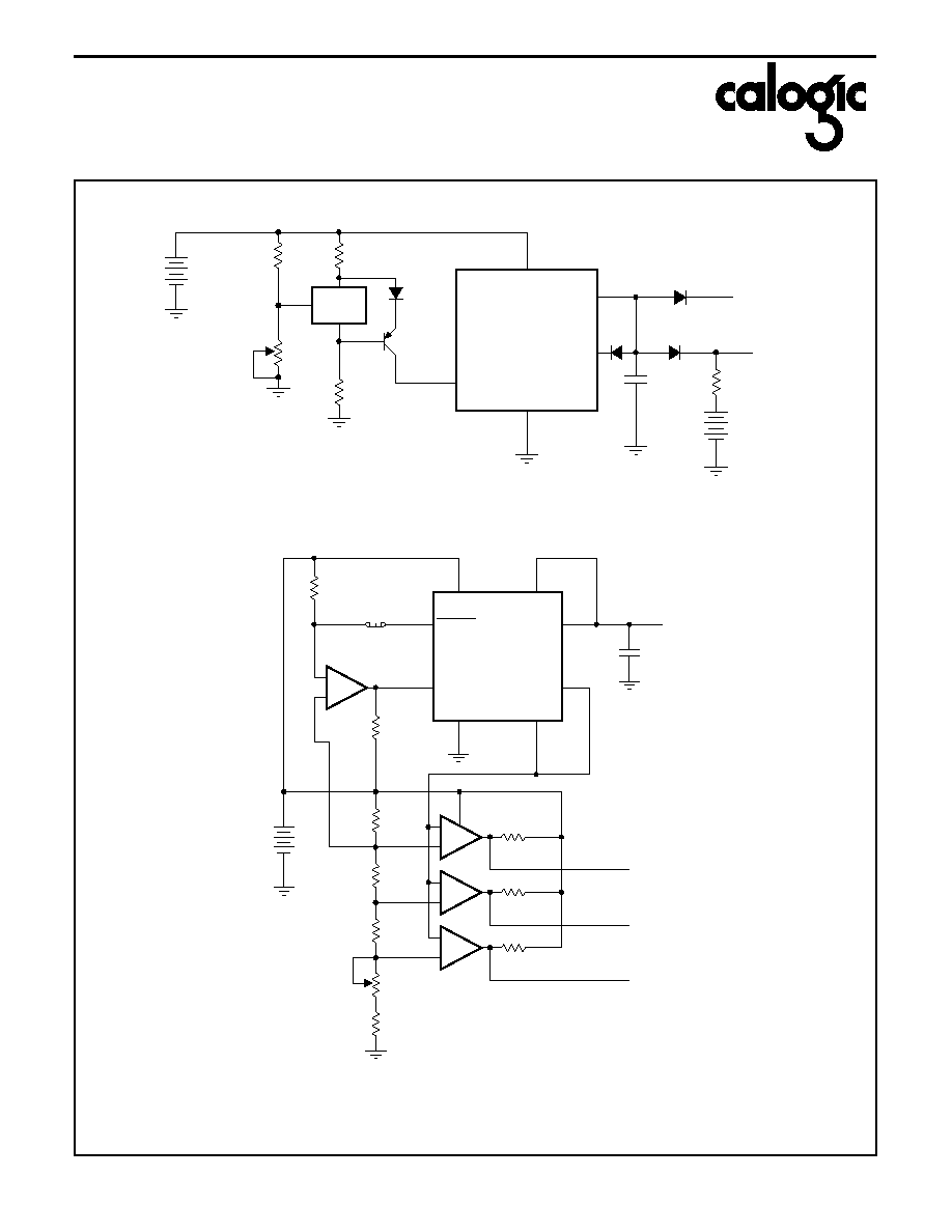
ERROR DETECTION COMPARATOR OUTPUT
The Comparator produces a logic low output whenever the
CLM2951 output falls out of regulation by more than around
5%. This is around 60mV offset divided by the 1.235
reference voltage. This trip level remains 5% below normal
regardless of the programmed output voltage of the regulator.
Figure 1 shows the timing diagram depicting the ERROR
signal and the regulator output voltage as the CLM2951 input
is ramped up and down. The ERROR signal becomes low at
around 1.3V input, and goes high around 5V input (input
voltage at which V
OUT
= 4.75). Since the CLM2951's dropout
voltage is load dependent, the input voltage trip point (around
5V) will vary with the load current. The output voltage trip
point (approx. 4.75V) does not vary with load.
The error comparator has an open-collector output which
requires an external pull-up resistor. Depending on the
system requirements the resistor may be returned to 5V
output or other supply voltage. In determining the value of
this resistor, note that the output is rated to sink 400
µ
A, this
value adds to battery drain in a low battery condition.
Suggested values range from 100K to 1M
. If the output is
unused this resistor is not required.
PROGRAMMING THE OUTPUT VOLTAGE OF CLM2951
The CLM2951 may be pin-strapped for 5V using its internal
voltage divider by tying Pin 1 (output) to Pin 2 (sense) and Pin
7 (feedback) to Pin 6 (5V Tap). Also, it may be programmed
for any output voltage between its 1.235V reference and its
30V maximum rating. As seen in Figure 2, an external pair of
resistors is required.
Refer to the below equation for the programming of the output
voltage:
V
OUT
= V
REF
◊
(1 + R
1
\R
2
) + I
FB
R
1
The V
REF
is 1.235 and I
FB
is the feedback bias current,
nominally -20nA. The minimum recommended load current of
1
µ
A forces an upper limit of 1.2M
on value of R
2
. If no load
is presented the I
FB
produces an error of typically 2% in V
OUT
which may be eliminated at room temperature by trimming R
1
.
To improve the accuracy choose the value of R2 = 100k this
reduces the error by 0.17% and increases the resistor
program current by 12
µ
A. Since the CLM2951 typically draws
60
µ
A at no load with Pin 2 open-circuited this is a small price
to pay.
REDUCING OUTPUT NOISE
It may be an advantage to reduce the AC noise present at the
output. One way is to reduce the regulator bandwidth by
increasing the size of the output capacitor. This is the only
way that noise can be reduced on CLM2950 but is relatively
inefficient, as increasing the capacitor from 1
µ
F to 220
µ
F only
decreases the noise from 430
µ
V to 160
µ
Vrms for a 100kHz
bandwidth at 5V output.
Noise could also be reduced fourfold by a bypass capacitor
across R
1
, since it reduces the high frequency gain from 4 to
unity.
C
BYPASS
1/2
R
1
◊
200Hz
or choose 0.01
µ
F. When doing this, the output capacitor must
be increased to 3.3
µ
F to maintain stability. These changes
reduce the output noise from 430
µ
V to 100
µ
Vrms for a
100kHz bandwidth at 5V output. With the bypass capacitor
added, noise no longer scales with output voltage so that
improvements are more dramatic at higher voltages.
CLM2950 / CLM2951
CORPORATION
CALOGIC CORPORATION, 237 Whitney Place, Fremont, California 94539, Telephone: 510-656-2900, FAX: 510-651-3025
CLM2950 / CLM2951
CORPORATION
CALOGIC CORPORATION, 237 Whitney Place, Fremont, California 94539, Telephone: 510-656-2900, FAX: 510-651-3025
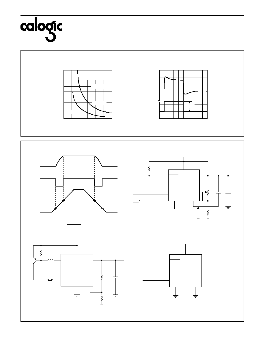
TEMPERATURE (∞C)
1.8
0.6
1.2
≠75
150
1D-49
SHUTDOWN
THRESHOLD VOLTAGE
SHUTDOWN THRESHOLD VOLTAGE (V)
0.8
1.0
1.4
1.6
≠50 ≠25 0
25 50 75 100 125
INPUT VOLTAGE (V)
180
0
0
30
1E-01
RATED
OUTPUT CURRENT
OUTPUT CURRENT (mA)
5
10
25
20
15
20
40
60
80
100
120
140
160
T
A
= 50∞C
T
A
= 85∞C
T
A
= 25∞C
V
OUT
= 5V
8-PIN SOIC
SOLDERED
TO PC BOARD
T
JMAX
= 125∞C
INPUT VOLTAGE (V)
30
≠10
1D-50
LINE REGULATION
OUTPUT VOLTAGE CHANGE (mV)
0
0
10
10
20
≠5
5
5
15
25
30
25
20
15
10
5
T
J
= 150∞C
T
J
= 125∞C
I
L
= 100
µ
A
I
L
= 1mA
I
L
= 100
µ
A
TYPICAL PERFORMANCE CHARACTERISTICS
TIME (mS)
125
100
µ
A
10
1E-02
LOAD TRANSIENT
RESPONSE
LOAD CURRENT
25
100mA
75
OUTPUT VOLTAGE
CHANGE (mV)
8
6
4
2
0
100
50
0
≠25
≠50
C
L
= 4.7
µ
F
V
OUT
= 5V
TIME (
µ
s)
1E-04
ENABLE TRANSIENT
SHUTDOWN
PIN VOLTAGE (V)
OUTPUT
VOLTAGE (V)
≠100
700
0
100 200 300 400 500 600
7
≠2
0
2
0
1
2
3
4
5
6
C
L
= 1.5
µ
F
V
OUT
= 5V
C
L
= 10
µ
F
V
IN
= 8V
I
L
= 10mA
TIME (mS)
80
100
µ
A
20
1E-03
LOAD TRANSIENT
RESPONSE
LOAD CURRENT
0
100mA
40
OUTPUT VOLTAGE
CHANGE (mV)
16
12
8
4
0
60
20
≠20
≠40
≠60
C
L
= 15
µ
F
V
OUT
= 5V
INPUT VOLTAGE (V)
1E-05
ERROR
COMPARATOR OUTPUT
COMPARATOR OUTPUT (V)
0
6
1
2
5
4
3
8
≠2
6
4
2
0
V
OUT
= 5V
NOTE: PULLUP RESISTOR
TO SEPARATE 5V SUPPLY
HYSTERESIS
400mV
4V
800
1E-07
LINE TRANSIENT
RESPONSE
INPUT
VOLTAGE
0
200
400
600
0
8V
6V
200mV
≠50mV
OUTPUT VOLTAGE
CHANGE
= 5V
C
L
= 4.7
µ
F
I
L
= 1mA
V
OUT
2.5
0.0
0.0
0.9
1E-06
COMPARATOR
SINK CURRENT
SINK CURRENT (mA)
0.1 0.2 0.3 0.4 0.5 0.6 0.7 0.8
2.0
1.5
1.0
0.5
T
A
= 125∞C
T
A
= 25∞C
T
A
= ≠55∞C
CLM2950 / CLM2951
CORPORATION
CALOGIC CORPORATION, 237 Whitney Place, Fremont, California 94539, Telephone: 510-656-2900, FAX: 510-651-3025
2.2
1.6
150
1E-08
MINIMUM
OPERATING VOLTAGE
≠50
0
50
100
2.0
1.8
1.7
2.1
1.9
MINIMUM OPERATING VOLTAGE (V)
TEMPERATURE (∞C)
≠25
25
75
125
≠75
INPUT VOLTAGE (V)
160
0
0
8
1E-10
GROUND PIN CURRENT
QUIESCENT CURRENT (
µ
A)
1
2
3
4
5
6
7
20
40
60
100
120
140
80
I
L
= 1mA
I
L
= 0
TEMPERATURE (∞C)
5.06
4.94
5.0
≠75
150
1E-09
OUTPUT VOLTAGE vs
TEMPERATURE OF 3
REPRESENTATIVE UNITS
OUTPUT VOLTAGE (V)
4.96
4.98
5.02
5.04
≠50 ≠25 0
25 50 75 100 125
0.2%
FREQUENCY (Hz)
1E-11
OUTPUT IMPEDANCE
OUTPUT IMPEDANCE (OHMS)
10
0.01
10
1M
100
1K
100K
10K
0.1
1
0.02
0.05
0.2
0.5
2
5
C
L
= 4.7
µ
F
I
O
= 100
µ
A
I
O
= 1mA
I
O
= 100mA
V
OUT
= 5V
FREQUENCY (Hz)
90
20
1E-13
RIPPLE REJECTION
RIPPLE REJECTION (dB)
80
70
60
50
40
30
10
6
10
5
10
4
10
3
10
2
10
1
I
L
= 1mA
C
L
= 1.5
µ
F
V
IN
= 6V
I
L
= 10mA
V
OUT
= 5V
FREQUENCY (Hz)
90
20
1E-12
RIPPLE REJECTION
RIPPLE REJECTION (dB)
80
70
60
50
40
30
10
6
10
5
10
4
10
3
10
2
10
1
C
L
= 1.5
µ
F
I
L
= 0
I
L
= 100
µ
A
V
OUT
= 5V
V
IN
= 6V
FREQUENCY (Hz)
80
10
1E-14
RIPPLE REJECTION
RIPPLE REJECTION (dB)
70
60
50
40
30
20
10
6
10
5
10
4
10
3
10
2
10
1
C
L
= 1.5
µ
F
V
IN
= 6V
V
OUT
= 5V
I
L
= 50
µ
A
I
L
= 100mA
TEMPERATURE (∞C)
≠75
150
1E-16
DIVIDER RESISTANCE
PIN 2 TO PIN 4 RESISTANCE (k
)
≠50 ≠25 0
25 50 75 100 125
400
0
100
300
200
FREQUENCY (Hz)
3.5
0.0
1E-15
OUTPUT NOISE
VOLTAGE NOISE
SPECTRAL DENSITY (
µ
V/ Hz)
3.0
2.5
2.0
1.5
1.0
0.5
10
5
10
2
10
4
10
3
I
L
= 100mA
C
L
= 4.7
µ
F
C
L
= 3.3
µ
F
0.01mF
BYPASS
PIN 1 TO
PIN 7
C
L
= 220
µ
F
TYPICAL PERFORMANCE CHARACTERISTICS (continued)
CLM2950 / CLM2951
CORPORATION
CALOGIC CORPORATION, 237 Whitney Place, Fremont, California 94539, Telephone: 510-656-2900, FAX: 510-651-3025
INPUT VOLTAGE (V)
150
0
0
30
1E-17
RAISED OUTPUT
OUTPUT CURRENT (mA)
5
10
25
20
15
20
40
60
80
100
120
140
160
TO-92 PACKAGE
.25∞ LEADS SOLDERED
TO PC BOARD
T
A
= 85∞C
T
A
= 25∞C
T
JMAX
= 125∞C
180
TIME (
µ
S)
5
≠1
0
50
1E-18
THERMAL RESPONSE
4
2
0
≠2
1
0
30
40
20
10
POWER
DISSIPATION (W)
OUTPUT VOLTAGE
CHANGE (mV)
1.25W
TYPICAL PERFORMANCE CHARACTERISTICS (continued)
1E-19
*SEE APPLICATION INFO.
OUTPUT
VOLTAGE
INPUT
VOLTAGE
4.75V
ERROR*
1.3V
5.0V
R
1
+V
IN
CLM2951
FB
4
1E-20
SD
GND
V
OUT
7
ERROR
8
1
3
R
2
ERROR
OUTPUT
SHUTDOWN
INPUT
3.3
µ
F
+
+V
IN
1.2 TO 30V
1.23V
.01
µ
F
100K
5
V
REF
TYPICAL APPLICATIONS
R
1
+V
IN
CLM2951
FB
4
1E-21
SD
GND
V
OUT
7
ERROR
8
1
+V
IN
1
µ
F
+
3
V
OUT
470K
470K
R
2
LATCH OFF WHEN ERROR FLAG OCCURS
5
*V
OUT
= V
IN
+V
IN
CLM2951
FB
4
1E-22
SD
GND
V
OUT
7
ERROR
OUTPUT
SHUTDOWN
INPUT
ERROR
8
1
+V
IN
*MINIMUM INPUT - OUTPUT VOLTAGE RANGES FROM 4mV TO 400mV.
DEPENDING ON LOAD CURRENT. CURRENT LIMIT IS TYPICALLY 160mA.
WIDE INPUT VOLTAGE RANGE CURRENT LIMITER
5
3
FIGURE 1. ERROR OUTPUT TIMING
FIGURE 2. ADJUSTABLE REGULATOR
CLM2950 / CLM2951
CORPORATION
CLM2951
4
1E-23
GND
8
1
3
SENSE
MAIN V-
MEMORY V+
NI-CAD
BACKUP
BATTERY
CLM385
6V
SEALED
LEAD-
ACID
BATTERY
SOURCE
100K
1.5K
120K
400K
20K
FB
IN457
SD
V
OUT
+V
IN
FOR 5.5V
LOW BATTERY DISCONNECT
+
1
µ
F
+
+V
IN
CLM2951
TAP
4
1E-24
SD
GND
V
OUT
6
ERROR
8
1
1
µ
F
+
3
+V
OUT
39k
100k
100k
100k
≠
+
C4
2
SENSE
= 5V
7
39k
100k
1k
1k
10k
20k
<6.2V**
<6.0V**
<5.8V**
1%
1%
1%
1%
5
R
3
6V
LEAD-
ACID
BATTERY
REGULATOR WITH STATE-OF-CHARGE INDICATOR
RESET
≠
+
C1
≠
+
C2
≠
+
C3
*OPTIONAL LATCH OFF WHEN DROPOUT OCCURS. ADJUST R3 FOR C2 SWITCHING WHEN V IS 6.0V.
**OUTPUTS GO LOW WHEN V DROPS BELOW DESIGNATED THRESHHOLDS.
IN
IN
TYPICAL APPLICATIONS (continued)
CALOGIC CORPORATION, 237 Whitney Place, Fremont, California 94539, Telephone: 510-656-2900, FAX: 510-651-3025
CALOGIC CORPORATION, 237 Whitney Place, Fremont, California 94539, Telephone: 510-656-2900, FAX: 510-651-3025
+V
IN
CLM2951
FB
4
1E-25
GND
8
5
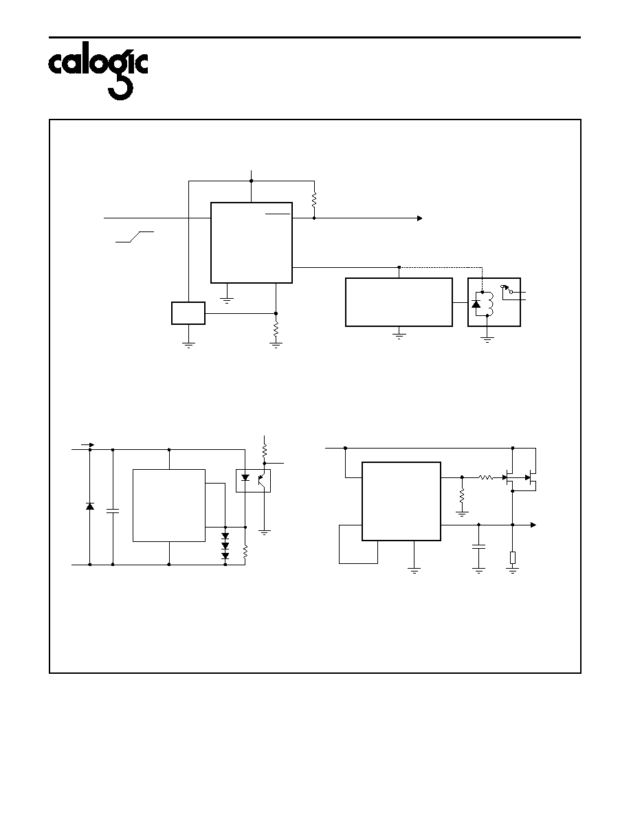
SYSTEM OVER TEMPERATURE PROTECTION CIRCUIT
AUX SHUTDOWN
INPUT
+V
IN
AS35
5 DEGREE SHUTDOWN FLAG
V
OUT
1
EXTERNAL CIRCUIT
PROTECTED FROM
OVER TEMPERATURE
(V+ GOES OFF WHEN
TEMP > 125)
OR
TEMP
SENSOR
7
+
≠
3
ERROR
SD
10K
ON
OFF
RELAY
8.2K
TYPICAL APPLICATIONS (continued)
CLM2951
4
1E-26
GND
8
1
OPEN CIRCUIT DETECTOR FOR 4mA TO 20mA CURRENT LOOP
7
FB
2
4
20mA
IN4001
360K
0.1
µ
F
IN457
OUTPUT
4.7mA
+5v
MIN VOLTAGE = 4V
+V
IN
V
OUT
CLM2951
4.7
µ
F
LOAD 50mA
TO 300mA
OUTPUT
5V
1
2
SENSE
GND
5
UNREGULATED INPUT
3
300mA REGULATOR WITH 0.75 DROPOUT
7
4
2N5432
27K
330K
IN
1E-27
V
TAP
FB
V
OUT
+
CLM2950 / CLM2951
CORPORATION

ERROR
GND
SHDN
5V TAP
SENSE
OUT
FEEDBACK
IN
R25
2.8
k
R23 60k
R21 8
R24
50k
R16
30k
R15
100k
R17
10
R13
100
k
R14
350
k
R22
150k
R17
12k
R28
60k
R27
182k
R18
20k
R26
60k
50k
10k
R3
50k
R4
13k
R30
30k
R5
180
k
R6
140
k
R9
27.8k
R2
50k
R1
20k
R8
31.4k
R10
150
k
R12
110
k
R11
18
k
R11
20.6
k
Q1
Q30 Q31
Q19
Q18
Q29
Q28
Q22
Q21
Q20
Q34
Q40
Q41
Q42
Q13
Q12
Q3
Q4
Q7
Q8
Q9
Q6
Q15A
Q15B
Q16
Q17
Q14
Q25
Q24
Q23
Q11
Q38
Q37
Q36
Q39
Q26
Q2
Q5
C1
20pF
C2
40pF
1E-28
10
SCHEMATIC DIAGRAM
CLM2950 / CLM2951
CORPORATION
Information furnished by Calogic is believed to be accurate and reliable. However, no responsibility is assumed for its use: nor for any infringement of patents or other
rights of third parties which may result from its use. No license is granted by implication or otherwise under any patent rights of Calogic.
CALOGIC CORPORATION
, 237 Whitney Place, Fremont, California 94539, Telephone: 510-656-2900, FAX: 510-651-3025