 | –≠–ª–µ–∫—Ç—Ä–æ–Ω–Ω—ã–π –∫–æ–º–ø–æ–Ω–µ–Ω—Ç: CLM4121 | –°–∫–∞—á–∞—Ç—å:  PDF PDF  ZIP ZIP |

High Speed Buffer
CLM4121 / CLM4321
FEATURES
∑
∑
High Slew Rate. . . . . . . . . . . . . . . . . . . . . . . . . . 2000V/
µ
s
∑
∑
Wide Bandwidth. . . . . . . . . . . . . . . . . . . . . . . . . . 180MHz
∑
∑
Peak Output Current . . . . . . . . . . . . . . . . . . . . . . . 300mA
∑
∑
Low Supply Current . . . . . . . . . . . . . . . . . . . . . . . . . 7mA
∑
∑
No Oscillations with Capacitive Loads
∑
∑
5V to
±
15V Operation Guaranteed
∑
∑
Fully Specified to Drive 50
Lines
APPLICATIONS
∑
∑
Coaxial Cable Driver
∑
∑
Flash A/D Converter Driver
∑
∑
Video DAC Buffer
∑
∑
OP Amp Booster
∑
∑
Video Amplifier
∑
∑
High Frequency Filter
∑
∑
Wide Bandwidth Signal Conditioning
∑
∑
Radar
∑
∑
Sonar
GENERAL DESCRIPTION
The CLM4121 family are high speed unity gain buffers that
slew at 2000V/
µ
s, having a small signal bandwidth of
180MHz, delivers 150mA, yet draws only 7mA supply current.
The fast slew rate, wide bandwidth, and high output drive
make the CLM4121 family the ideal choice for closed loop
buffer applications with wide band op amps.
These same characteristics are the excellent choices for open
loop applications such as driving coaxial and switched pair
cables.
ORDERING INFORMATION
Part
Package
Temperature Range
CLM4121 N
NO8A (Plastic P Dip 8 Lead) -40
o
C to 85
o
C
CLM4121 M
MO8B (SOIC 8 Lead)
-40
o
C to 85
o
C
CLM4321 N
NO8A (Plastic P Dip 8 Lead) -25
o
C to 70
o
C
CLM4321 M
MO8B (SOIC 8 Lead)
-25
o
C to 70
o
C
CORPORATION
CONNECTION DIAGRAMS
1
2
3
4
5
6
7
8
Plastic SO
V
N/C
*V-
V-*
V+
V
*Heat-sinking pins. Pin 1 and Pin 8
must be connected to the negative supply.
IN
OUT
*V-
V-*
1
2
3
4
5
6
7
8
Plastic DIP
*V-
N/C
V-*
V+
V-*
*V-
V
IN
V
OUT
*Heat-sinking pins. Pin 1 and Pin 8
must be connected to the negative supply.
Package NO8A
Package MO8B
CALOGIC CORPORATION
, 237 Whitney Place, Fremont, California 94539, Telephone: 510-656-2900, FAX: 510-651-1076
ABSOLUTE MAXIMUM RATINGS (Note 1)
Supply Voltage. . . . . . . . . . . . . . . . . . . . . . . . . . . . . . . . . .
±
20
Input Voltage . . . . . . . . . . . . . . . . . . . . . . . . . . . . . .
±
Vsupply
Storage Temperature Range . . . . . . . . . . . . -65
o
C to +150
o
C
Lead Temperature
(Soldering 10 seconds) . . . . . . . . . . . . . . . . . . . . . . 260
o
C
Power Dissipation . . . . . . . . . . . . . . . . . . . . . . . . . . . (Note 4)
ESD Tolerance (Note 3). . . . . . . . . . . . . . . . . . . . . . .
±
2000V
Thermal Resistance (
JA
) (Note 6)
N Package . . . . . . . . . . . . . . . . . . . . . . . . . . . . . . . 50
o
C/W
M Package . . . . . . . . . . . . . . . . . . . . . . . . . . . . . . . 60
o
C/W
Maximum Junction Temperature . . . . . . . . . . . . . . . . . . 150
o
C
CORPORATION
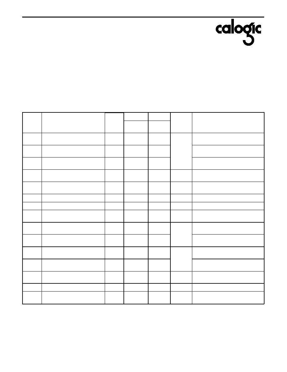
DC ELECTRICAL CHARACTERISTICS
The following specifications apply for Supply Voltage =
±
15V, V
CM
= 0, R
L
100K
and R
S
= 50
unless otherwise noted.
Boldface limits apply for T
A
= T
J
= T
MIN
to T
MAX
; all other limits T
A
= T
J
= 25
o
C.
SYMBOL
CHARACTERISTICS
TYP
CLM4121
CLM4321
UNITS
CONDITIONS
Limit
(Note 5)
Limit
(Note 5)
A
V1
Voltage Gain 1
0.970
0.950
0.950
0.950
0.950
V/V Min
R
L
= 1K
, V
IN
=
±
10V
A
V2
Voltage Gain 2
0.900
0.800
0.800
0.800
0.800
R
L
= 50
, V
IN
=
±
6V
A
V3
Voltage Gain 3
0.840
0.780
0.750
0.750
0.700
R
L
= 50
, V
+
= 5V
V
IN
= 2V
PP
V
OS
Offset Voltage
15
20
30
30
30
mV Max
R
L
= 1K
I
B
Input Bias Current
1
5
7
10
10
µ
A Max
R
L
= 1K
, R
S
= 10k
,
R
IN
Input Resistance
0.5
.2
.2
M
R
L
= 50
C
IN
Input Capacitance
3.5
pF
R
O
Output Resistance
3
5
10
5
6
Max
I
OUT
=
±
10mA
I
S1
Supply Current 1
7.5
10
10
10
10
mA Max
R
L
=
I
S2
Supply Current 2
2.5
5
5
5
5
R
L
=
, V
+
= 5V
V
O1
Output Swing 1
13.5
13.3
13
13.2
13
±
V Min
R
L
= 1K
V
O2
Output Swing 2
12.7
10
9
10
9
R
L
= 100
V
O3
Output Swing 3
1.8
1.6
1.3
1.6
1.5
V
PP
Min
R
L
= 50
, V
+
= 5V (Note 5)
I
OUT
Output Current
200
140
140
mA
V
IN
=
±
13V
PSSR
Power Supply
Rejection Ratio
70
60
60
60
60
dB Min
V
±
=
±
5V to
±
15V
CLM4121 / CLM4321
CALOGIC CORPORATION
, 237 Whitney Place, Fremont, California 94539, Telephone: 510-656-2900, FAX: 510-651-1076

CORPORATION
AC ELECTRICAL CHARACTERISTICS
The following specifications apply for Supply Voltage =
±
15V, V
CM
= 0, R
L
100K
and R
S
= 50
unless otherwise noted.
Boldface limits apply for T
A
= T
J
= T
MIN
to T
MAX
; all other limits T
A
= T
J
= 25
o
C.
SYMBOL
CHARACTERISTICS
TYP
CLM4121
CLM4321
UNITS
CONDITIONS
Limit (Note 5)
Limit (Note 5)
SR
1
Slew Rate 1
4000
3500
2500
V/
µ
s
V
IN
=
±
11V, R
L
= 1K
(Note 2)
SR
2
Slew Rate 2
2000
1500
1000
V
IN
=
±
5V, R
L
= 50
(Note 2)
SS
BW
Small Signal Bandwidth
180
140
100
MHz
V
IN
=
±
100mV
PP
, R
L
= 50
C
L
10pF
LS
BW
Large Signal Bandwidth
65
55
40
V
IN
=
±
11V, R
L
= 1K
C
L
10pF
P
BW
Power Bandwidth
40
30
20
V
IN
=
±
8V, R
L
= 50
C
L
10pF
t
r
, t
f
Rise Time
Fall Time
2.0
2.5
3.5
ns
R
L
= 50
, C
L
10pF
V
O
= 100mV
PP
t
pd
Propagation Delay Time
3.0
ns
R
L
= 50
, C
L
10pF
V
O
= 100mV
PP
O
S
Overshoot
10
%
R
L
= 50
, C
L
10pF
V
O
= 100mV
PP
Note 1: Absolute Maximum Ratings indicate limits beyond which damage to the device may occur. DC and AC electrical specifications do not
apply when operating the device beyond its rated operating conditions.
Note 2: Slew rate is measured with 50
source impedance at 25
o
C. For accurate measurements, the input slew rate should be at least
5000V/
µ
s.
Note 3: The test circuit consists of the human body model of 120pF in series with 1500
.
Note 4: The maximum power dissipation is a function of T
J(max),
JA
and T
A
. The maximum allowable power dissipation at any ambient
temperature is P
D
= (T
J(max)
- T
A
)/
JA
.
Note 5: Limits are guaranteed by testing, correlation or periodic characterization.
Note 6: For M & N package,
JA
is measured by soldering the unit directly on a printed circuit board and V
-
pins are connected to 2 square
inches of 2 oz copper.
CLM4121 / CLM4321
CALOGIC CORPORATION
, 237 Whitney Place, Fremont, California 94539, Telephone: 510-656-2900, FAX: 510-651-1076

CORPORATION
TYPICAL PERFORMANCE CHARACTERISTICS
FREQUENCY (MHz)
1
10
2
5
BANDWIDTH
(LARGE SIGNAL & POWER)
20
50
400
100 200
24
18
12
6
0
30
V
IN
(V )
P-
P
R
L
= 50
R
L
= 10K
SUPPLY VOLTAGE (±V)
2
SUPPLY VOLTAGE
vs BANDWIDTH
0
-3dB BANDWIDTH (M
Hz)
4
6
8
10 12 14 16 18 20
300
280
260
240
220
200
180
160
140
120
100
80
60
40
20
R
L
= 50
R
L
= 1K
SUPPLY VOLTAGE (±V)
1
SUPPLY VOLTAGE
vs SUPPLY CURRENT
0
S
U
PPLY C
U
R
R
E
N
T
(±
m
A
)
3
5
7
9 11 13 15 17
11
10
9
8
7
6
5
4
3
2
1
19
INPUT VOLTAGE
vs SLEW RATE
0.0
4500
SL
E
W
R
A
TE (V
/
µ
s)
V
IN
(V )
P-P
2
6
10
14
18
22
4000
3500
3000
2500
2000
1500
1000
500
R
L
= 50
R
L
= 1K
FREQUENCY (MHz)
GAI
N
(dB)
1
10
2
5
FREQUENCY RESPONSE
PH
ASE
LAG
(D
EGREE
S
)
20
50
400
100 200
0
-2
-4
-6
-8
64
48
32
16
0
80
R
L
= 1K
V
IN
100mV
C
L
10pF
T
j
= 25∞C
FREQUENCY (MHz)
GAI
N
(dB)
1
10
2
5
FREQUENCY RESPONSE
PH
ASE
LAG
(D
EGREE
S
)
20
50
400
100 200
0
-2
-4
-6
-8
80
60
40
20
0
R
L
= 50
V
IN
100mV
C
L
10pF
T
j
= 25∞C
CLM4121 / CLM4321
CALOGIC CORPORATION
, 237 Whitney Place, Fremont, California 94539, Telephone: 510-656-2900, FAX: 510-651-1076

CORPORATION
(1.27)
1
2
5
6
7
8
3
4
(TOP VIEW)
.213
.205
(5.4)
(5.2)
.050
.020
.013
(.50)
(.33)
.210
.205
(5.32)
(5.19)
.074
.070
(1.87)
(1.77)
.318
.302
(8.10)
(7.64)
.010
.006
(.25)
(.15)
.010
.004
(.25)
(.10)
.023
.019
MO8B-8 LEAD SOIC
(.58)
(.48)
MO8B DIMENSIONS
CALOGIC CORPORATION
, 237 Whitney Place, Fremont, California 94539, Telephone: 510-656-2900, FAX: 510-651-1076
CORPORATION
(0.58)
(0.36)
0.070
0.030
(1.78)
(0.76)
0.015
0.290
(0.38)
(0.20)
0.310
0.220
(7.87)
(5.59)
0.320
0.290
(8.13)
(7.37)
(1.40)
(10.29)
0.405 MAX
15 MAX
o
(1.13)
0.005
MAX
0.055
MAX
0.150
(3.81)
0.06
0.15
(1.52)
(0.38)
MAX
0.200
(5.08)
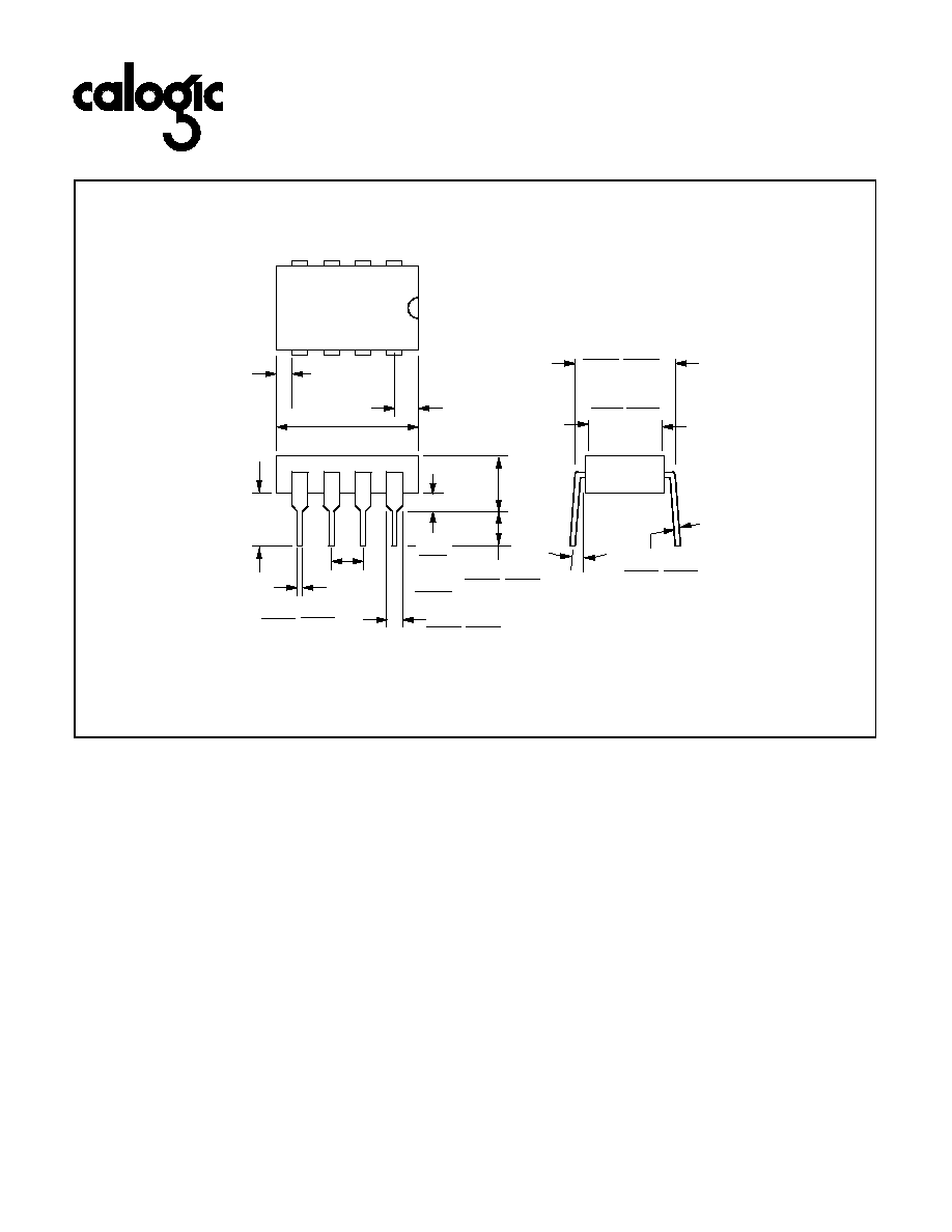
8-Pin Plastic Dip
0.023
0.014
(millimeters)
All Dimensions in
inches and
MIN
0.200
0.125
(5.08)
(3.18)
NO8A DIMENSIONS
CALOGIC CORPORATION
, 237 Whitney Place, Fremont, California 94539, Telephone: 510-656-2900, FAX: 510-651-1076