150mA Low-Noise LDO
Voltage Regulator
CLM5205
FEATURES
∑
∑
Ultra-Low Noise Output
∑
∑
High Output Voltage Accuracy
∑
∑
Guaranteed 150mA Output
∑
∑
Low Quiescent Current
∑
∑
Low Dropout Voltage
∑
∑
Extremely Tight Load and Line Regulation
∑
∑
Very Low Temperature Coefficient
∑
∑
Current and Thermal Limiting
∑
∑
Reverse-Battery Protection
∑
∑
"Zero" OFF-Mode Current
∑
∑
Logic-Controlled Electronic Enable
APPLICATIONS
∑
∑
Cellular Telephones
∑
∑
Laptop, Notebook, and Palmtop Computers
∑
∑
Battery Powered Equipment
∑
∑
PCMCIA V
CC
and V
PP
Regulation/Switching
∑
∑
Consumer/Personal Electronics
∑
∑
SMPS Post-Regulator/ DC toDC Modules
∑
∑
High Efficiency Linear Power Supplies
GENERAL DESCRIPTION
The Calogic CLM5205 is a low noise, low dropout voltage
regulator featuring ultra low ground current (800uA at 100mA
output) and tighter than 1% initial accuracy with a logic
compatible ON/OFF switching input. Designed for hand-held
battery powered devices, the CLM505 is switched by a CMOS
or TTL compatible logic signal. When disabled, power
consumption drops nearly to zero. Prolonging battery life, the
ground current of the CLM5205 increases only slightly in
dropout. Major features of the CLM5205 include a reference
bypass pin for excellent low-noise performance, protection
against reversed battery, current limiting, and overtemperature
shutdown.
The CLM5202 is available in several fixed voltages and an
adjustable output voltage version in a small SOT-23-5
package. The pinout is smaller to the LP2980 with
significantly better performance.
ORDERING INFORMATION
Part
Voltage
Package
Temperature
Range
CLM5205M
Adjustable SOT-23-5
-40
o
C to +125
o
C
CLM5205M-5.0
5.0V
SOT-23-5
-40
o
C to +125
o
C
CLM5205M-4.7
4.7V
SOT-23-5
-40
o
C to +125
o
C
CLM5205M-4.0
4.0V
SOT-23-5
-40
o
C to +125
o
C
CLM5205M-3.6
3.6V
SOT-23-5
-40
o
C to +125
o
C
CLM5205M-3.3
3.3V
SOT-23-5
-40
o
C to +125
o
C
CLM5205M-3.0
3.0V
SOT-23-5
-40
o
C to +125
o
C
CLM5205M-2.85
2.85V
SOT-23-5
-40
o
C to +125
o
C
CORPORATION
1V-15
GND
EN
V
IN
V
OUT
1
µ
F
+
+
0.01
µ
F
REF. BYP
(OPT.)
CALOGIC CORPORATION,
237 Whitney Place, Fremont, California 94539, Telephone: 510-656-2900, FAX: 510-651-3025
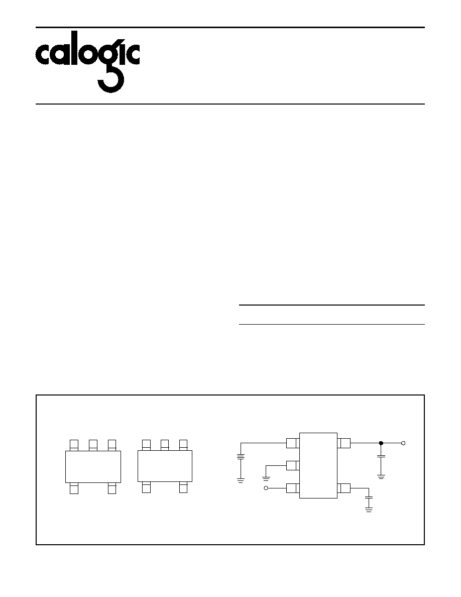
PIN CONFIGURATION
TYPICAL APPLICATION
3
EN
2
GND
IN
V
1
REF BYP
4
CLM5205M-XX
1V-13
V
OUT
5
3
EN
2
GND
IN
V
1
ADJ
4
CLM5205M
(ADJUSTABLE)
1V-14
V
OUT
5

ABSOLUTE MAXIMUM RATINGS
Absolute Maximum Ratings indicate limits beyond which
damage to the device may occur. Electrical specifications do
not apply when operating the device beyond its specified
Operating Ratings.
Power Dissipation . . . . . . . . . . . . . . . . . . . . . Internally Limited
Lead Temperature (Soldering 5 seconds) . . . . . . . . . . . 260
o
C
Operating Junction Temperature Range . . . . -40
o
C to +125
o
C
Input Supply Voltage . . . . . . . . . . . . . . . . . . . . . . -20V to +20V
ENABLE Input Voltage . . . . . . . . . . . . . . . . . . . . -20V to +20V
RECOMMENDED OPERATING CONDITIONS
Input Voltage . . . . . . . . . . . . . . . . . . . . . . . . . . . . . 2.5V to 16V
Operating Junction Temperature Range . . . . -40
o
C to +125
o
C
ENABLE Input Voltage. . . . . . . . . . . . . . . . . . . . . . . . 0V to V
IN
SOT-23-5
JA
. . . . . . . . . . . . . . . . . . . . . . . . . . . . . See Note 1
DC ELECTRICAL CHARACTERISTICS
Limits in standard typeface are for T
J
= 25
o
C and limits in boldface apply over the junction temperature range of -40
o
C to +125
o
C.
Unless otherwise specified, V
IN
= V
OUT
+ 1V, I
L
= 100
µ
A, C
L
= 3.3
µ
F, and V
ENABLE
2.0V.
SYMBOL
PARAMETER
MIN
TYP
MAX
UNITS
CONDITIONS
V
O
Output Voltage Accuracy
-1
-2
1
2
%
Variation from specified V
OUT
V
O
T
Output Voltage
Temperature Coeficient
40
ppm/
o
C
(Note 2)
V
O
V
O
Line Regulation
0.004
%
V
IN
= V
OUT
+ 1V to 16V
V
O
V
O
Load Regulation
0.04
%
I
L
= 0.1mA to 150mA (Note 3)
V
IN
- V
O
Dropout Voltage
(Note 4)
17
80
115
140
165
mV
I
L
= 100
µ
A
I
L
= 20mA
I
L
= 50mA
I
L
= 100mA
I
L
= 150mA
I
GND
Quiescent Current
< 1
µ
A
V
ENABLE
0.7V (Shutdown)
I
GND
Ground Pin Current
(Note 5)
80
160
350
720
1300
µ
A
V
ENABLE
2.0V , I
L
= 100
µ
A
I
L
= 20mA
I
L
= 50mA
I
L
= 100mA
I
L
= 150mA
PSRR
Ripple Rejection
75
dB
I
LIMIT
Current Limit
320
mA
V
OUT
= 0V
V
O
P
D
Thermal Regulation
0.05
%/W
(Note 6)
e
no
Output Noise
260
nV/
Hz
I
L
= 50mA, C
L
= 4.7
µ
F, 0.01
µ
F from Ref BYP to ground
ENABLE INPUT
V
IL
Input Voltage Level
Logic Low
Logic High
2.0
0.4
V
OFF
ON
I
L
I
IH
ENABLE Input Current
0.01
2
µ
A
V
IL
0.18V
V
IH
2.0V
CLM5205
CORPORATION
CALOGIC CORPORATION,
237 Whitney Place, Fremont, California 94539, Telephone: 510-656-2900, FAX: 510-651-3025

CLM5205
CORPORATION
Information furnished by Calogic is believed to be accurate and reliable. However, no responsibility is assumed for its use: nor for any infringement of patents or other
rights of third parties which may result from its use. No license is granted by implication or otherwise under any patent rights of Calogic.
CALOGIC CORPORATION,
237 Whitney Place, Fremont, California 94539, Telephone: 510-656-2900, FAX: 510-651-3025
Note 1: Absolute maximum ratings indicate limits beyond which damage to the components may occur. Electrical specifications do not apply
when operating the device outside of its rated operating conditions. The maximum allowable power dissipation is a function of the maximum
junction temperature, TJ(MAX), the junction-to-ambient thermal resistance,
JA
, and the ambient temperature, T
A
. The maximum allowable power
dissipation at any ambient temperature is calculated using: P
(MAX)
= (T
J(MAX)
- T
A
)
JA
. Exceeding the maximum allowable power dissipation will
result in excessive die temperature, and the regulator will go into thermal shutdown. The
JA
of the MIC5205-xxBM5 (all versions) is 250
o
C/W
mounted on a PC board.
Note 2: Output voltage temperature coefficient is defined as the worst case voltage change divided by the total temperature range.
Note 3: Regualtion is measured at constant junction temperature using low duty cylce pulse testing. Parts are tested for load regualtion in the
load range for 0.1mA to 150mA.
Note 4: Dropout Voltage is defined as the input to output differential at which the output voltage drops 2% below its normal value measured at 1V
differential.
Note 5: Ground pin current is the regulator quiescent current plus pass transistor base current. The total current drawn from the supply is the
sum of the load current plus the ground pin current.
Note 6: Thermal regulation is defined as the change in output voltage at a time T after a change in power dissipation is applied, excluding load or
line regulation effects. Specifications are for a 150mA load pulse at V
IN
= 16V for T = 10ms.