 | –≠–ª–µ–∫—Ç—Ä–æ–Ω–Ω—ã–π –∫–æ–º–ø–æ–Ω–µ–Ω—Ç: CVA2403 | –°–∫–∞—á–∞—Ç—å:  PDF PDF  ZIP ZIP |

Low Cost
Triple CRT Driver
CVA2403T
FEATURES
∑
∑
Rise/Fall Time. . . . . . . . . . . . . . . . . . . . . . . . . . . . . . . 4.0ns
∑
∑
Swing . . . . . . . . . . . . . . . . . . . . . . . . . . . . . . . . . . . 65V
P-P
∑
∑
Supply Voltage . . . . . . . . . . . . . . . . . . . . . . . . . . . . . . . 90V
∑
∑
High Input Impedance
APPLICATIONS
∑
∑
CRT driver for up to 82kHz monitors
∑
∑
Excellent Gray Scale Linearity
∑
∑
Emitter Peaking Option
∑
∑
Adjustable Gain
DESCRIPTION
The CVA2403T is a high input impedance wideband triple
amplifier. The device is specifically designed to drive a CRT
featuring a high speed buffer for easy matching to a pre-amplifier,
no crossover distortion for excellent gray scale linearity, external
emitter peaking to maximize the high frequency gain at the cross
hatch pattern and an adjustable gain for ease of use. This
device can drive monitors with resolutions of 1280 X 1024
(interlaced) with pixel frequencies of 220MHz.
The part is housed in the industry standard 11-lead TO-220
molded power package. The heat sink is grounded.
ORDERING INFORMATION
Part
Package
Temperature
CVA2403T
T11A
-20
o
C to +100
o
C
CORPORATION
CONNECTION DIAGRAM AND SIMPLIFIED SCHEMATIC
OUT
OUT
11
10
9
8
7
6
5
4
3
2
1
IN
TOP VIEW
T11A PACKAGE
V
V
V
Gain/Peaking
Control
V
BIAS
V
CC
1N-22
OUT
V
IN
V
Gain/Peaking
Control
Gain/Peaking
Control
IN
V
GND = TAB
1
2
3
3
3
2
2
1
1
CALOGIC CORPORATION, 237 Whitney Place, Fremont, California 94539, Telephone: 510-656-2900, FAX: 510-651-3025
1P-38
GND
TAB
7
9
V
CC
11,10,8
12
12
V
BIAS
V
OUT
1,3,5
V
IN
2,4,6
Gain/Peaking
Control
= 1000
R
1
Preliminary Data Sheet

ABSOLUTE MAXIMUM RATINGS
Supply Voltage. . . . . . . . . . . . . . . . . . . . . . . . . . . . . . . . . . 90V
Power Dissipation . . . . . . . . . . . . . . . . . . . . . . . . . . . . . . . 16W
Storage Temperature . . . . . . . . . . . . . . . . . . . -25
o
C to +100
o
C
Operating Temperature . . . . . . . . . . . . . . . . . -20
o
C to +100
o
C
Lead Temperature . . . . . . . . . . . . . . . . . . . . . . . . . . . . +300
o
C
CVA2403T
CORPORATION
FIGURE 1. TEST CIRCUIT
GND
TAB
1P-39
V
IN
V
BIAS
C1 = 0.01
µ
F
C2 = 100
µ
F
C3 = 0.1
µ
F
C7 = 120pF
D1, D2 = FHD400
R1 = 62
R2 = 20
C4 = 100
µ
F
C6 = 8pF
R2
R1
C6
C4
C3
C2
C1
D2
D1
VIDEO
INPUT
V 9
CC
1,3,5
7
8,10,11
V
OUT
C7
V
P G
2,4,6
TEKTRONIX
FET PROBE
MODEL 6201
(CAP. 1.5pF)
CVA2403T
DC ELECTRICAL CHARACTERISTICS V
s
= 80V, C
L
= 8pF, DC
INPUT BIAS
= 12V, V
IN
= 3.4V, V
OUT
= 50V
p-p
. T
CASE
= +25
o
C.
See Figure 1.
SYMBOL
CHARACTERISTICS
MIN
TYP
MAX
UNITS
I
cc
Supply Current
30
34
40
mA
V
OUT DC
Output DC Level
40
45
50
V
A
v
Voltage Gain
13
15
17
V
Gain Matching
0.2
dB
AC ELECTRICAL CHARACTERISTICS V
s
= 80V, C
L
= 8pF, DC
INPUT BIAS
= 12V, V
IN
= 3.4V, V
OUT
= 50V
p-p
. T
CASE
= +25
o
C.
See Figure 1.
SYMBOL
CHARACTERISTICS
MIN
TYP
MAX
UNITS
T
r
Rise Time
4
4.5
ns
T
f
Fall Time
4
4.5
ns
L
e
Linearity
6
%
OS
Overshoot
5
%
CALOGIC CORPORATION, 237 Whitney Place, Fremont, California 94539, Telephone: 510-656-2900, FAX: 510-651-3025

CVA2403T
CORPORATION
CALOGIC CORPORATION, 237 Whitney Place, Fremont, California 94539, Telephone: 510-656-2900, FAX: 510-651-3025
FIGURE 2. APPLICATION CIRCUIT
1P-40
GND
TAB
V
BIAS
C1 = 0.01
µ
F
C2 = 100
µ
F
C3 = 0.1
µ
F
C4 = 100
µ
F
C5 = 2.2
µ
F
C7 = 40 - 120pf
D1, D2 = FHD400
L = 330 - 390nH
R1 = 62
R2 = 20
R3 = 47
R4 = 47(1/2W)
R7 = 33
R8 = 39
R10 = 680
R3
R4
C4
C3
C2
C1
D2
D1
V 9
CC
7
8,10,11
V
OUT
C5
SPARK
GAP
CVA2403T
R5
L
V
IN
R2
R1
VIDEO
INPUT
1,3,5
C7
V
PG
2,4,6
DC BIAS
APPLICATION INFORMATION
The CVA2403T is a high voltage triple CRT driver suitable for
VGA, Super VGA, IBM
Æ
8514, 1280 x 1024 and 1024 x 768
non-interlaced display applications. The CVA2403T features
80V operation. The part is housed in the industry standard 11
lead TO-220 molded power package. The heat sink is floating
and may be grounded for ease of manufacturing and RFI
shielding.
Thermal Considerations
The transfer characteristics of the amplifier are shown in
Figure 4. Since this is a class A input stage, power supply
current increases as the input signal increases and
consequently power dissipation also increases.
The CVA2403T cannot be used without heat sinking.
Figure 2
shows the power dissipated in each channel over the
operating voltage range of the device. Under white screen
conditions, i.e.: 20V output, dissipation increases to 16W
total. The CVA2403T case temperature must be maintained
below +90
o
C. If the maximum expected ambient temperature
is +50
o
C, then a heat sink is needed with thermal resistance
equal to or less than:
R
th
=
(
90
-
50
o
C
)
16W
=
2.5
o
C/W
The CVA2403T maximum load is 600
to ground or V
+
.
The output of CVA2403T is not short circuit proof. Any resistance
to V
+
or Ground should be > 600
.
FIGURE 3. CVA2403T DC Characteristics
INPUT VOLTAGE
OUTPUT VOLTAGE (VOLTS)
0
60
90
3
5
7
POWER DISSIPATION (WATTS)
1
4
6
2
50
80
40
70
30
20
10
3
4
2
1
5
100
110
6
VOLTAGE
POWER
1G-26
CVA2403T
CORPORATION
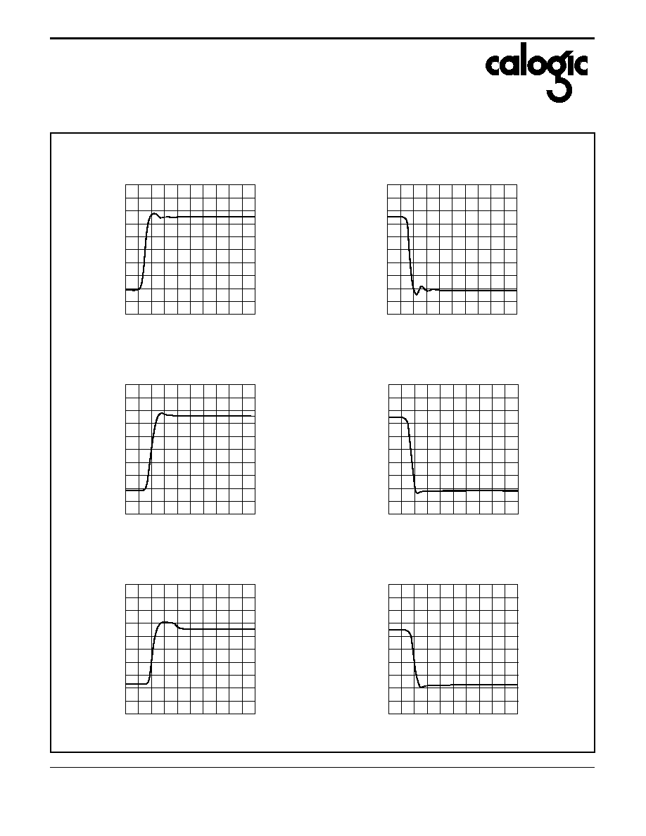
10ns/DIV
8V/DIV
30V
10V
1D-03
FALL TIME
WITH PEAKING
INDUCTOR & CAPACITOR
10ns/DIV
8V/DIV
30V
10V
1D-02
RISE TIME
WITH PEAKING
INDUCTOR & CAPACITOR
10ns/DIV
8V/DIV
90V
10V
1D-05
FALL TIME
WITH PEAKING
CAPACITOR (NO INDUCTOR)
10ns/DIV
8V/DIV
90V
10V
1D-04
RISE TIME
WITH PEAKING
CAPACITOR (NO INDUCTOR)
TYPICAL CHARACTERISTICS
10ns/DIV
10V/DIV
120.5V
2.5V
1D-07
FALL TIME
NO PEAKING
INDUCTOR OR CAPACITOR
10ns/DIV
10V/DIV
120.5V
2.5V
1D-06
RISE TIME
NO PEAKING
INDUCTOR OR CAPACITOR
Information furnished by Calogic is believed to be accurate and reliable. However, no responsibility is assumed for its use: nor for any infringement of patents or other
rights of third parties which may result from its use. No license is granted by implication or otherwise under any patent rights of Calogic.
CALOGIC CORPORATION, 237 Whitney Place, Fremont, California 94539, Telephone: 510-656-2900, FAX: 510-651-3025

CVA2401T
CORPORATION