
HB01U 11/98 REV B
Page 1
Product Data Sheet
1 W
ATT
U
NREGULATED
DC/DC C
ONVERTERS
HB01U
FEATURES
G
G
G
G
G HIGH ISOLATION
G
G
G
G
G 2500Vrms ISOLATION TEST VOLTAGE
G
G
G
G
G BARRIER 100% PRODUCTION TESTED
G
G
G
G
G LOW BARRIER CAPACITANCE - 10pF
G
G
G
G
G LOW LEAKAGE CURRENT - 2�A MAX
G
G
G
G
G 24-PIN DIP AND SMD
G
G
G
G
G INTERNAL FILTERING
G
G
G
G
G NON-CONDUCTIVE CASE
G
G
G
G
G LOW COST
G
G
G
G
G LOW PROFILE - .375"
APPLICATIONS
G
G
G
G
G INDUSTRIAL PROCESS CONTROL
G
G
G
G
G DC MOTOR DRIVE
G
G
G
G
G INTRINSIC SAFETY SYSTEMS
G
G
G
G
G GROUND LOOP ELIMINATION
G
G
G
G
G MEDICAL EQUIPMENT
G
G
G
G
G PORTABLE TEST EQUIPMENT
G
G
G
G
G DATA ACQUISITION
Internet: http://www.cdpowerelectronics.com
Power Electronics Division, United States
3400 E Britannia Drive, Tucson, Arizona 85706
Phone: 800.547.2537 Fax: 520.770.9369
Power Electronics Division, Europe
C&D Technologies (Power Electronics) Ltd.
132 Shannon Industrial Estate, Shannon, Co. Clare, Ireland
Tel: +353.61.474.133 Fax:+353.61.474.141
DESCRIPTION
The HB01U Series offers a wide selection of input and
output voltages to choose from. Each model is offered in
a 24-pin DIP or SMD package and has an input to output
isolation rating of 2500Vrms making it ideal for applica-
tions requiring high isolation. The dielectric withstand
characteristics of each converter are measured in pro-
duction to ensure barrier integrity.
The HB01U Series is ideal for applications where the
output is susceptible to high voltage transients, such as
motor drive and industrial process control applications.
The low barrier capacitance gives excellent input to
output dV/dt characteristics thus protecting the input
control circuitry from peak transients appearing on the
output.
The HB01U Series uses a self-oscillating circuit design
technology to realize low cost and high performance. The
inherent current limiting capability of the high isolation
design reduces high current stresses during start-up thus
increasing the capacitive load capability while maintain-
ing high reliability.
As with all of our DC/DC converters, surface mount
construction combined with extensive qualification test-
ing assures low cost without sacrificing quality and reli-
ability.

HB01U 11/98 REV B
Page 2
NOMINAL
RATED
RATED
INPUT CURRENT
INPUT
OUTPUT
OUTPUT
VOLTAGE
VOLTAGE CURRENT MIN LOAD
RATED LOAD EFFICIENCY
MODEL
(V
DC
)
(V
DC
)
(mA)
(mA)
(mA) (%)
HB01U05S05
5
5
200
63
290
68
HB01U05S12
5
12
83
63
290
70
HB01U05S15
5
15
67
63
290
73
HB01U12S05
12
5
200
20
120
68
HB01U12S12
12
12
83
20
120
70
HB01U12S15
12
15
67
20
114
73
HB01U15S05
15
5
200
25
98
68
HB01U15S12
15
12
83
25
95
70
HB01U15S15
15
15
67
25
90
73
HB01U24S05
24
5
200
13
61
68
HB01U24S12
24
12
83
13
60
70
HB01U24S15
24
15
67
13
57
73
HB01U05D05
5
�5
�100
63
290
68
HB01U05D12
5
�12
�42
63
285
70
HB01U05D15
5
�15
�34
63
275
73
HB01U12D05
12
�5
�100
20
123
68
HB01U12D12
12
�12
�42
20
118
70
HB01U12D15
12
�15
�34
20
114
73
HB01U15D05
15
�5
�100
25
98
68
HB01U15D12
15
�12
�42
25
95
70
HB01U15D15
15
�15
�34
25
90
73
HB01U24D05
24
�5
�100
13
61
68
HB01U24D12
24
�12
�42
13
60
70
HB01U24D15
24
�15
�34
13
57
73
PARAMETER
CONDITIONS
MIN
TYP
MAX
UNITS
INPUT
Voltage Range
4.5
5
5.5
V
DC
10.8
12
13.2
V
DC
13.5
15
16.5
V
DC
20
24
30
V
DC
Reflected Ripple Current
35
mAp-p
ISOLATION
Rated Voltage
3535
VDC
Test Voltage
60 Hz, 10 Seconds
2500
Vrms
Resistance
10
G
Capacitance
10
pF
Leakage Current
V
ISO
= 240V
AC
, 60Hz
1
2
�Arms
OUTPUT
Rated Power
1
W
Voltage Setpoint Accuracy
�3
�5
%
Temperature Coefficent
�0.02
%/�C
Ripple & Noise
BW = DC to 10MHz
50
mVp-p
BW =10Hz to 2MHz
25
mVrms
Line Regulation
High Line to Low Line
�1.5
%/% Vin
Load Regulation
See Performance Curves (Min Load =1mA)
GENERAL
Switching Frequency
160
kHz
Package Weight
12
g
MTTF per MIL-HDBK-217, Rev. F
Circuit Stress Method
Ground Benign
T
A
= +25�C
2,000,000
Hr
TEMPERATURE
Specification
-25
+70
�C
Operation
-40
+85
�C
Storage
-40
+110
�C
Specifications typical at T
A
= +25�C, nominal input voltage, rated output current unless otherwise specified.
COMMON SPECIFICATIONS
Specifications typical at T
A
= +25�C, nominal input voltage, rated output current unless otherwise specified.
ELECTRICAL SPECIFICATIONS
HB01U 11/98 REV B
Page 3
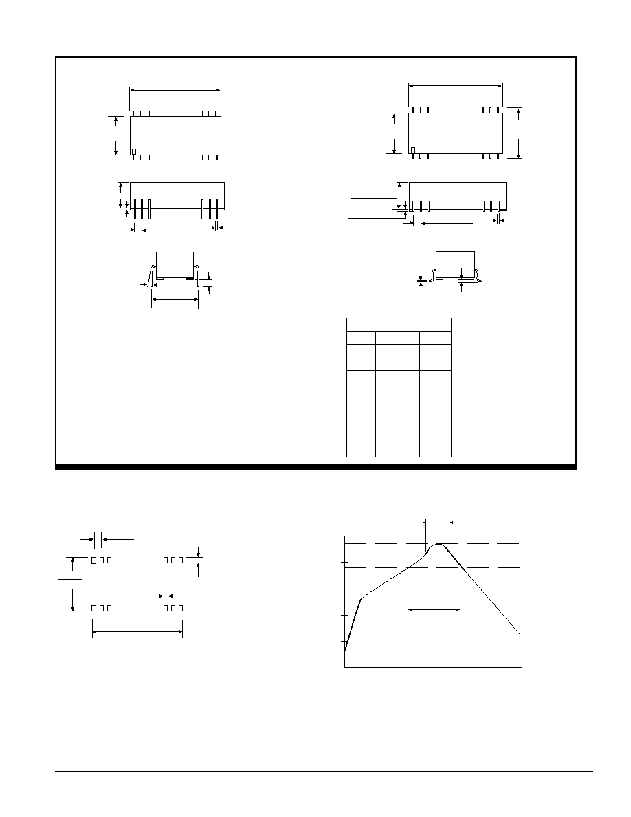
MECHANICAL
Package/Pinout "Y" and "Z"
0.100�0.010"
(2.54�0.25)
0.020�0.002"
(0.51�0.05)
0.015�0.005"
(0.38�0.13)
0.375�0.005"
(9.52�0.13)
1.285�0.010"
(32.64�0.25)
24 23 22
15 14 13
12
11
10
3
2
1
0.014�0.002"
(0.36�0.05)
.015�.010"
(.38�.25)
0.525�0.010"
(13.34�0.25)
0.695�0.015"
(17.65�0.38)
0�-
15�
0.125+0.030"
-0.000"
(3.18+0.76)
( -0.00)
0.600"
(15.24)
0.100�0.010"
(2.54�0.25)
0.020�0.002"
(0.51�0.05)
0.015�0.005"
(0.38�0.13)
0.375�0.005"
(9.52�0.13)
1.285�0.010"
(32.64�0.25)
24 23 22
15 14 13
12
11
10
3
2
1
0.525�0.010"
(13.34�0.25)
SIDE VIEWS
TOP VIEWS
END VIEWS
SMD PACKAGE
DIP PACKAGE
HB01UxxyzzY
HB01UxxyzzZ
NU = Do Not Use.
NC = No Internal Connection.
Duplicate pin functions are internally connected.
All dimensions are in inches (millimeters).
GRID: 0.100 inches (2.54 millimeters)
Typically Marked with: specific model ordered, date code, job code and Logo.
PIN CONNECTIONS
PIN# SINGLES DUALS
1
+V
OUT
+V
OUT
2
-V
OUT
Common
3
NU
-V
OUT
10
-V
IN
-V
IN
11
NC
NC
12
+V
IN
+V
IN
13
+V
IN
+V
IN
14
NC
NC
15
-V
IN
-V
IN
21
NC
NC
22
NU
-V
OUT
23
-V
OUT
Common
24
+V
OUT
+V
OUT
RECOMMENDED LAND PATTERN
24 23 22
15 14 13
12
11
10
3
2
1
0.730"
(18.54)
1.150"
(29.21)
0.100"
(2.54)
0.080"
(2.03)
0.040"
(1.02)
50
100
150
200
250
TEMPERA
T
URE (
�
C)
TIME (seconds)
235 �C MAX
220
190
30 sec MAX
(>220�C)
90 sec MAX
(>190�C)
RECOMMENDED REFLOW PROFILE
MATERIAL: Units are encapsulated in a low thermal resistance molding
compound which has excellent chemical resistance, wide operating
temperature range, and good electrical properties under high humidity
environments. The encapsulant and outer shell of the unit have UL94V-0
ratings. Lead material is brass with a solder plated surface to allow ease of
solderability.

HB01U 11/98 REV B
Page 4
HB01U xxyzz Y/Z /H
ABSOLUTE MAXIMUM RATINGS
Internal Power Dissipation...................................................0.5 Watt
Short Circuit Duration...............................................................5 Min
Lead Temperature (soldering, 10 seconds max)..................+300�C
*Note: Refer to Reflow Profile for SMD Models.
*
ORDERING INFORMATION
Device Family
HB Indicates DC/DC Converter
Model Number
Where:
xx = Input Voltage
y = Number or Outputs (Single "S", Dual "D")
zz = Output Voltage
Package Option
Screening Option
T
YPICAL PERFORMANCE CURVES
Specifications typical at T
A
= +25�C, nominal input voltage, rated output current unless otherwise specified.
VOUT VS LOAD
(5Vout Models)
VOUT VS LOAD
(�5Vout Models)
VOUT VS LOAD
(12Vout Models)
VOUT VS LOAD
(�12Vout Models)
VOUT VS LOAD
(15Vout Models)
VOUT VS LOAD
(�15Vout Models)
EFFICIENCY VS LOAD
1
20
80
150
200
5.3
5.5
5.7
5.9
4.9
5.1
1
10
30
50
70
12.2
12.3
12.4
12.5
12.6
12.7
1
20
40
80
100
5.0
5.2
5.4
5.6
5.8
6.0
1
10
20
30
40
12.0
12.1
12.2
12.3
12.4
12.5
14.9
15.0
15.1
15.2
15.3
15.4
1
10
20
60
67
1
10
20
30
34
14.9
15.0
15.1
15.2
15.3
15.4
20
60
80
100
30
40
50
60
70
80
V
out (V
olts)
V
out (V
olts)
V
out (V
olts)
V
out (V
olts)
V
out (V
olts)
V
out (V
olts)
Ef
ficiency (%)
Load (mA)
Load (mA)
Load (mA)
Load (mA)
Load (mA)
Load (mA)
Load (mA)
100
60
90
5
40
5
40
The information provided herein is believed to be reliable; however, C&D TECHNOLOGIES assumes no responsibility for inaccuracies or omissions. C&D TECHNOLOGIES assumes no responsibility
for the use of this information, and all use of such information shall be entirely at the user's own risk. Prices and specifications are subject to change without notice. No patent rights or licenses to any
of the circuits described herein are implied or granted to any third party. C&D TECHNOLOGIES does not authorize or warrant any C&D TECHNOLOGIES product for use in life support devices/systems
or in aircraft control applications.