 | –≠–ª–µ–∫—Ç—Ä–æ–Ω–Ω—ã–π –∫–æ–º–ø–æ–Ω–µ–Ω—Ç: CM1213 | –°–∫–∞—á–∞—Ç—å:  PDF PDF  ZIP ZIP |

1
© Copyright 2002, Capella Microsystems, Inc.
399B West Trimble Road, San Jose, CA 95131 USA ∑ 408.382.6600 ∑ FAX.408.382.6601
CM1213
Integrated PD+TIA
DESCRIPTION
The Capella CM1213 PDIC is a low voltage
integrated photodiode and transimpedence
amplifier (TIA) for use as the photodetector in
CD optical pickups. The built-in TIA has low
output impedance for stability. The CM1213
can also be used in quadruple-speed drives
because the photodiode and TIA can operate
at typical speeds of 8MHz.
10
9
8
7
6
1
3
4
5
+
-
+
-
2
GND
E
OUT
D
OUT
A
OUT
NC
B
OUT
C
OUT
F
OUT
Vcc
Vc
D
D IV AMP
F
F IV AMP
+
-
A
A IV AMP
R1
R1
R2
+
-
B
B IV AMP
R1
+
-
+
-
C
C IV AMP
E
E IV AMP
R1
R2
R1 = 88K
, R2 = 182k
A~F Photodiodes
FEATURES
∑ Low voltage operation (2.5V ~ 5.5V)
∑ Built-in TIA (current-to-voltage
conversion circuit)
∑ High PD sensitivity
∑ Recommended Diode for CD
applications is an IR laser diode
(=780nm)
∑ Supports Focus Servo (Astigmatism
method) and Tracking servo (Three
beam method)
APPLICATIONS
∑ Optical pickups for VideoCD-players,
CD-ROM, CD-MP3 players, and CD-
Audio
DISCLAIMER
Capella Microsystems Inc. reserves the right to make changes in specifications or discontinue this product at any time
without notice. Please contact Capella Microsystems Inc. for possible updates before starting a design.
Capella Microsystems Inc. products are not designed for use in life support applications. Any parties who use these products
in such applications do so at their own risk and agree to fully indemnify Capella Microsystems Inc. for any damages resulting
from such improper usage or sale.
Revision: 0.1
Date: 03-Dec-2002

CM1213 -- Integrated PD+TIA
2
© Copyright 2002, Capella Microsystems, Inc.
CM1213 Pin Descriptions
Pin No.
Symbol
I/O
Equivalent Circuit
Description
1
2
4
5
D
OUT
A
OUT
B
OUT
C
OUT
O
Output of electrical signals
converted from optical
signals
3 NC
Common with GND for the
package construction
6
10
E
OUT
F
OUT
O
Output of electrical signals
converted from optical
signals
7
GND
I
Single power supply: GND
8 Vc
I
Single power supply: center
voltage input
9 Vcc
I
Positive
power
supply

CM1213 -- Integrated PD+TIA
3
© Copyright 2002, Capella Microsystems, Inc.
Absolute Maximum Ratings (Ta = 25∞∞∞∞C)
Operating Conditions
Electrical & Optical Characteristics
(Vcc = 5V, Vs = 2.5V, Ta = 25∞∞∞∞C)
* Note 1: The CM1213 is based on a single power supply
* Note 2: Vc must be able to sink / source
±
500
µ
A
* Note 3: Dark Condition. There is no light incident on the photodiodes
* Note 4: The output voltage and the output offset voltage are with respect to Vc
* Note 5: The maximum output voltage is with respect to GND
* Note 6: The output voltage parameters and the frequency characteristics are guaranteed by design
Description Symbol
Value
Unit
Power Supply Voltage
Vcc
7.0
V
Operating Temperature
Topr
-20 ~ +75
∞C
Storage Temperature
Tstg
-40 ~ +85
∞C
Allowable Power Dissipation
P
D
200 mW
Description Signal
Condition
Min
Typ
Max
Unit
Supply Voltage (* Note 1)
Vcc
-
2.5
5.0
5.5
V
Reference Voltage (* Note 2)
Vc
Vcc/2
1.25
2.5
2.75
V
Description
Signal Condition Min
Typ
Max
Unit
Applicable
to
Current Consumption
Icc
(*Note 3)
-
6.0
8.0
mA
Vcc
Output Offset Voltage
Voff
Offset voltage with
Respect to Vc
(*Note 3)
-15 0 +15 mV A
OUT
~ F
OUT
(A+B) ≠ (C+D)
(*Note 3)
-20 0 +20 mV A
OUT
~ D
OUT
(A+D) ≠ (B+C)
(*Note 3)
-20 0 +20 mV A
OUT
~ D
OUT
(A+C) - (B+D)
(*Note 3)
-20 0 +20 mV A
OUT
~ D
OUT
Output Offset
Voltage Difference
Voff
(E - F)
(*Note 3)
-15 0 +15 mV E
OUT
~ F
OUT
Output Voltage (A-D)
Vo
Po = 10µW, =780nm
290 370 450 mV A
OUT
~ D
OUT
Output Voltage (E-F)
Vo
Po = 10µW, =780nm
610 770 930 mV E
OUT
~ F
OUT
Max. Output Voltage (A-D)
Vomax
Po = 100µW, =780nm
4.0 4.2 -
V A
OUT
~ D
OUT
Max. Output Voltage (E-F)
Vomax
Po = 100µW, =780nm
4.0 4.2 -
V E
OUT
~ F
OUT
Cutoff Frequency (A-D)
fc
100KHz, -3dB
6.0
8.0
-
MHz
A
OUT
~ D
OUT
Cutoff Frequency (E-F)
fc
10KHz, -3dB
100
400
KHz
E
OUT
~ F
OUT
CM1213 -- Integrated PD+TIA
4
© Copyright 2002, Capella Microsystems, Inc.
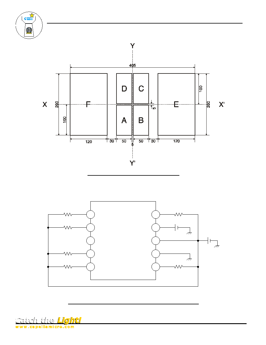
Figure 2: CM1213 Photodiode Layout
1
2
3
4
5
D
OUT
A
OUT
NC
B
OUT
C
OUT
10
9
8
7
6
F
OUT
Vcc
Vc
GND
E
OUT
10k
10k
10k
10k
10k
10k
C1
C2
Note: C1 and C2 are 0.1uF capacitors
Figure 3: CM1213 Test Measurement Circuit Diagram

CM1213 -- Integrated PD+TIA
5
© Copyright 2002, Capella Microsystems, Inc.
Figure 4: CM1213 CMP Package Dimensions
Figure 5: CM1213 COB Package Dimensions