CAT28C257
1
CAT28C257
256K-Bit CMOS PARALLEL EEPROM
FEATURES
s
Fast read access times: 120/150 ns
s
Low power CMOS dissipation:
Active: 25 mA max.
Standby: 150
µ
A max.
s
Simple write operation:
On-chip address and data latches
Self-timed write cycle with auto-clear
s
Fast write cycle time:
5ms max
s
CMOS and TTL compatible I/O
s
Automatic page write operation:
1 to 128 Bytes in 5ms
Page load timer
s
End of write detection:
Toggle bit
DATA
DATA
DATA
DATA
DATA
polling
s
Hardware and software write protection
s
100,000 Program/erase cycles
s
100 Year data retention
s
Commercial, industrial and automotive
temperature ranges
DESCRIPTION
The CAT28C257 is a fast, low power, 5V-only CMOS
Parallel EEPROM organized as 32K x 8-bits. It requires a
simple interface for in-system programming. On-chip
address and data latches, self-timed write cycle with auto-
clear and V
CC
power up/down write protection eliminate
additional timing and protection hardware.
DATA
Polling
and Toggle status bits signal the start and end of the self-
timed write cycle. Additionally, the CAT28C257 features
hardware and software write protection.
The CAT28C257 is manufactured using Catalyst's
advanced CMOS floating gate technology. It is designed
to endure 100,000 program/erase cycles and has a data
retention of 100 years. The device is available in JEDEC
approved 28-pin DIP or 32-pin PLCC packages.
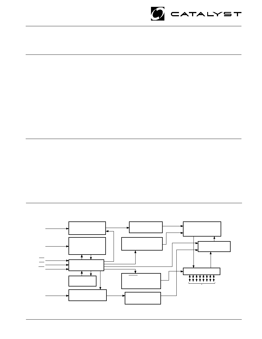
BLOCK DIAGRAM
5096 FHD F02
© 2002 by Catalyst Semiconductor, Inc.
Characteristics subject to change without notice
ADDR. BUFFER
& LATCHES
ADDR. BUFFER
& LATCHES
INADVERTENT
WRITE
PROTECTION
CONTROL
LOGIC
TIMER
ROW
DECODER
COLUMN
DECODER
HIGH VOLTAGE
GENERATOR
A7A14
CE
OE
WE
A0A6
I/O0I/O7
I/O BUFFERS
32,768 x 8
E
2
PROM
ARRAY
128 BYTE PAGE
REGISTER
VCC
DATA POLLING
AND
TOGGLE BIT
Doc. No. 1015, Rev. B
CAT28C257
2
Doc. No. 1015, Rev. B
5096 FHD F01
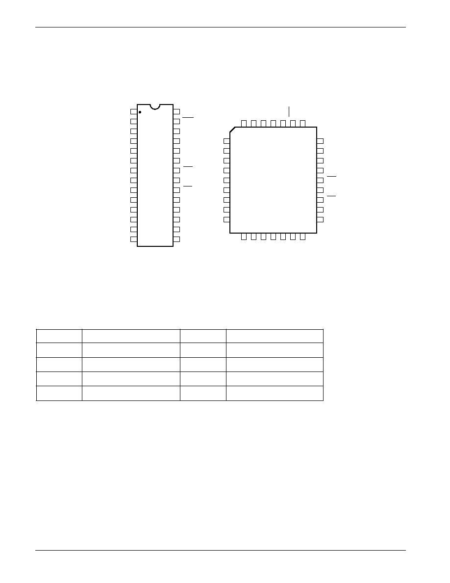
PIN CONFIGURATION
PLCC Package (N)
DIP Package (P)
I/O2
VSS
I/O6
I/O5
13
14
20
19
18
17
9
10
11
12
24
23
22
21
A1
A0
I/O0
I/O1
OE
A10
CE
I/O7
A5
A4
A3
A2
5
6
7
8
1
2
3
4
A14
A12
A7
A6
A9
A11
28
27
26
25
VCC
WE
A13
A8
A6
A5
A4
A3
5
6
7
8
A2
A1
A0
NC
9
10
11
12
I/O0
13
A8
A9
A11
NC
29
28
27
26
OE
A10
CE
25
24
23
22
I/O7
21
I/O
1
I/O
2
V
SS
NC
I/O
3
I/O
4
I/O
5
14 15 16 17 18 19 20
4
3
2
1 32 31 30
A
7
A
12
A
14
NC
V
CC
WE
A
13
I/O4
I/O3
16
15
I/O6
PIN FUNCTIONS
Pin Name
Function
A
0
A
14
Address Inputs
I/O
0
I/O
7
Data Inputs/Outputs
CE
Chip Enable
OE
Output Enable
Pin Name
Function
WE
Write Enable
V
CC
5V Supply
V
SS
Ground
NC
No Connect
CAT28C257
3
Doc. No. 1015, Rev. B
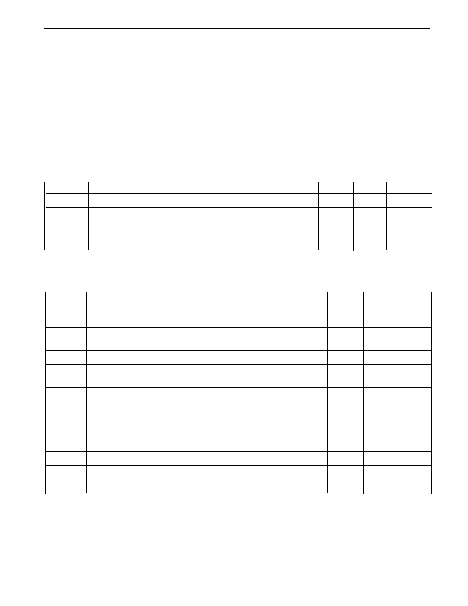
D.C. OPERATING CHARACTERISTICS
V
CC
= 5V
±
10%, unless otherwise specified.
Symbol
Parameter
Test Conditions
Min
Typ
Max
Units
I
CC
V
CC
Current (Operating, TTL)
CE
=
OE
= V
IL
, f=6MH
z
30
mA
All I/O's Open
I
CCC
(5)
V
CC
Current (Operating, CMOS)
CE
=
OE
= V
ILC
, f=6MH
z
25
mA
All I/O's Open
I
SB
V
CC
Current (Standby, TTL)
CE
= V
IH
, All I/O's Open
1
mA
I
SBC
(6)
V
CC
Current (Standby, CMOS)
CE
= V
IHC
,
150
µ
A
All I/O's Open
I
LI
Input Leakage Current
V
IN
= GND to V
CC
10
10
µ
A
I
LO
Output Leakage Current
V
OUT
= GND to V
CC
,
10
10
µ
A
CE = V
IH
V
IH
(6)
High Level Input Voltage
2
V
CC
+0.3
V
V
IL
(5)
Low Level Input Voltage
0.3
0.8
V
V
OH
High Level Output Voltage
I
OH
= 400
µ
A
2.4
V
V
OL
Low Level Output Voltage
I
OL
= 2.1mA
0.4
V
V
WI
Write Inhibit Voltage
3.5
V
*COMMENT
Stresses above those listed under "Absolute Maximum
Ratings" may cause permanent damage to the device.
These are stress ratings only, and functional operation
of the device at these or any other conditions outside of
those listed in the operational sections of this specifica-
tion is not implied. Exposure to any absolute maximum
rating for extended periods may affect device perfor-
mance and reliability.
ABSOLUTE MAXIMUM RATINGS*
Temperature Under Bias .................. -55
°
C to +125
°
C
Storage Temperature ........................ -65
°
C to +150
°
C
Voltage on Any Pin with
Respect to Ground
(2)
............ -2.0V to +V
CC
+ 2.0V
V
CC
with Respect to Ground ................ -2.0V to +7.0V
Package Power Dissipation
Capability (Ta = 25
°
C) ................................... 1.0W
Lead Soldering Temperature (10 secs) ............ 300
°
C
Output Short Circuit Current
(3)
........................ 100 mA
RELIABILITY CHARACTERISTICS
Symbol
Parameter
Test Method
Min
Typ
Max
Units
N
END
(1)
Endurance
MIL-STD-883, Test Method 1033 10
4
or 10
5
Cycles/Byte
T
DR
(1)
Data Retention
MIL-STD-883, Test Method 1008
100
Years
V
ZAP
(1)
ESD Susceptibility
MIL-STD-883, Test Method 3015
2000
Volts
I
LTH
(1)(4)
Latch-Up
JEDEC Standard 17
100
mA
Note:
(1) This parameter is tested initially and after a design or process change that affects the parameter.
(2) The minimum DC input voltage is 0.5V. During transitions, inputs may undershoot to 2.0V for periods of less than 20 ns. Maximum DC
voltage on output pins is V
CC
+0.5V, which may overshoot to V
CC
+2.0V for periods of less than 20 ns.
(3) Output shorted for no more than one second. No more than one output shorted at a time.
(4) Latch-up protection is provided for stresses up to 100mA on address and data pins from 1V to V
CC
+1V.
(5) V
ILC
= 0.3V to +0.3V.
(6) V
IHC
= V
CC
0.3V to V
CC
+0.3V.
CAT28C257
4
Doc. No. 1015, Rev. B
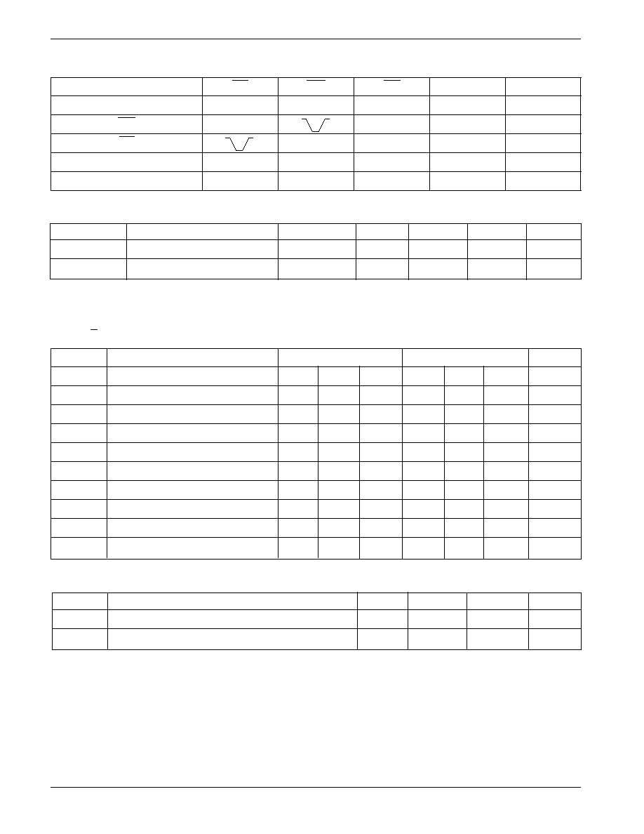
CAPACITANCE T
A
= 25
°
C, f = 1.0 MHz, V
CC
= 5V
Symbol
Test
Conditions
Min
Typ
Max
Units
C
I/O
(1)
Input/Output Capacitance
V
I/O
= 0V
10
pF
C
IN
(1)
Input Capacitance
V
IN
= 0V
6
pF
MODE SELECTION
Mode
CE
WE
OE
I/O
Power
Read
L
H
L
D
OUT
ACTIVE
Byte Write (WE Controlled)
L
H
D
IN
ACTIVE
Byte Write (CE Controlled)
L
H
D
IN
ACTIVE
Standby, and Write Inhibit
H
X
X
High-Z
STANDBY
Read and Write Inhibit
X
H
H
High-Z
ACTIVE
Note:
(1) This parameter is tested initially and after a design or process change that affects the parameter.
(2) Output floating (High-Z) is defined as the state when the external data line is no longer driven by the output buffer.
28C257-12
28C257-15
Symbol
Parameter
Min
Typ
Max
Min
Typ
Max
Units
t
RC
Read Cycle Time
120
150
ns
t
CE
CE
Access Time
120
150
ns
t
AA
Address Access Time
120
150
ns
t
OE
OE
Access Time
50
70
ns
t
LZ
(1)
CE
Low to Active Output
0
0
ns
t
OLZ
(1)
OE
Low to Active Output
0
0
ns
t
HZ
(1)(2)
CE
High to High-Z Output
50
50
ns
t
OHZ
(1)(2)
OE
High to High-Z Output
50
50
ns
t
OH
(1)
Output Hold from Address Change
0
0
ns
A.C. CHARACTERISTICS, Read Cycle
V
CC
=5V + 10%, Unless otherwise specified
Symbol
Parameter
Min
Typ
Max
Units
t
PUR
Power-Up to Read
100
µ
s
t
PUW
Power-Up to Write
5
10
ms
Power-Up Timing
CAT28C257
5
Doc. No. 1015, Rev. B
Note:
(1)
This parameter is tested initially and after a design or process change that affects the parameter.
(2)
Input rise and fall times (10% and 90%) < 10 ns.
(3)
A write pulse of less than 20ns duration will not initiate a write cycle.
(4)
A timer of duration t
BLC
max. begins with every LOW to HIGH transition of WE. If allowed to time out, a page or byte write will begin;
however a transition from HIGH to LOW within t
BLC
max. stops the timer.
5096 FHD F04
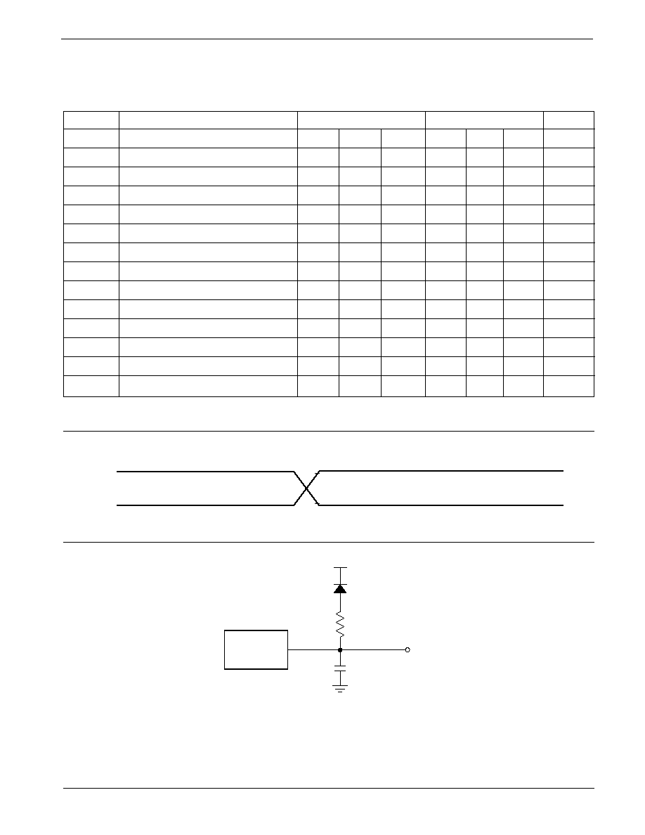
Figure 1. A.C. Testing Input/Output Waveform(2)
1.3V
DEVICE
UNDER
TEST
1N914
3.3K
CL = 100 pF
OUT
CL INCLUDES JIG CAPACITANCE
Figure 2. A.C. Testing Load Circuit (example)
INPUT PULSE LEVELS
REFERENCE POINTS
2.0 V
0.8 V
2.4 V
0.45 V
5096 FHD F03
A.C. CHARACTERISTICS, Write Cycle
V
CC
=5V
±
10%, unless otherwise specified
28C257-12
28C257-15
Symbol
Parameter
Min
Typ
Max
Min
Typ
Max
Units
t
WC
Write Cycle Time
5
5
ms
t
AS
Address Setup Time
0
0
ns
t
AH
Address Hold Time
50
50
ns
t
CS
CE
Setup Time
0
0
ns
t
CH
CE
Hold Time
0
0
ns
t
CW
(3)
CE
Pulse Time
100
100
ns
t
OES
OE
Setup Time
0
0
ns
t
OEH
OE
Hold Time
0
0
ns
t
WP
(3)
WE
Pulse Width
100
100
ns
t
DS
Data Setup Time
50
50
ns
t
DH
Data Hold Time
0
0
ns
t
INIT
(1)
Write Inhibit Period After Power-up
5
10
5
10
ms
t
BLC
(1)(4)
Byte Load Cycle Time
0.1
100
0.1
100
µ
s
CAT28C257
6
Doc. No. 1015, Rev. B
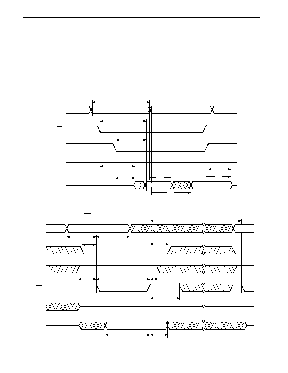
ADDRESS
CE
OE
WE
tRC
DATA OUT
DATA VALID
DATA VALID
tCE
tOE
tOH
tAA
tOHZ
tHZ
VIH
HIGH-Z
tLZ
tOLZ
DEVICE OPERATION
Read
Data stored in the CAT28C257 is transferred to the data
bus when
WE
is held high, and both
OE
and
CE
are
held low. The data bus is set to a high impedance state
when either
CE
or
OE
goes high. This 2-line control
architecture can be used to eliminate bus contention in
a system environment.
Byte Write
A write cycle is executed when both
CE
and
WE
are low,
and
OE
is high. Write cycles can be initiated using either
WE
or
CE
, with the address input being latched on the
falling edge of
WE
or
CE
, whichever occurs last. Data,
conversely, is latched on the rising edge of
WE
or
CE
,
whichever occurs first. Once initiated, a byte write cycle
automatically erases the addressed byte and the new
data is written within 5 ms.
Figure 3. Read Cycle
Figure 4. Byte Write Cycle [WE Controlled]
ADDRESS
CE
OE
WE
DATA OUT
tAS
DATA IN
DATA VALID
HIGH-Z
tCS
tAH
tCH
tWC
tOEH
tBLC
tDH
tDS
tOES
tWP
5096 FHD F06
28C257 F06
CAT28C257
7
Doc. No. 1015, Rev. B
Page Write
The page write mode of the CAT28C257 (essentially an
extended BYTE WRITE mode) allows from 1 to 128
bytes of data to be programmed within a single E
2
PROM
write cycle. This effectively reduces the byte-write time
by a factor of 128.
Following an initial WRITE operation (
WE
pulsed low, for
t
WP
, and then high) the page write mode can begin by
issuing sequential
WE
pulses, which load the address
and data bytes into a128 byte temporary buffer. The
page address where data is to be written, specified by
bits A
7
to A
14
, is latched on the last falling edge of
WE
.
Each byte within the page is defined by address bits A
0
to A
6
(which can be loaded in any order) during the first
and subsequent write cycles. Each successive byte load
cycle must begin within t
BLC MAX
of the falling edge of the
preceding
WE
pulse. There is no page write window
limitation as long as
WE
is pulsed low within t
BLC MAX
.
Upon completion of the page write sequence,
WE
must
stay high a minimum of t
BLC MAX
for the internal automatic
program cycle to commence. This programming cycle
consists of an erase cycle, which erases any data that
existed in each addressed cell, and a write cycle, which
writes new data back into the cell. A page write will only
write data to the locations that were addressed and will
not rewrite the entire page.
Figure 5. Byte Write Cycle [
CE
CE
CE
CE
CE
Controlled]
5096 FHD F07
Figure 6. Page Mode Write Cycle
OE
CE
WE
ADDRESS
I/O
tWP
tBLC
BYTE 0
BYTE 1
BYTE 2
BYTE n
BYTE n+1
BYTE n+2
LAST BYTE
tWC
5096 FHD F10
ADDRESS
CE
OE
WE
DATA OUT
tAS
DATA IN
DATA VALID
HIGH-Z
tAH
tWC
tOEH
tDH
tDS
tOES
tBLC
tCH
tCS
tCW
CAT28C257
8
Doc. No. 1015, Rev. B
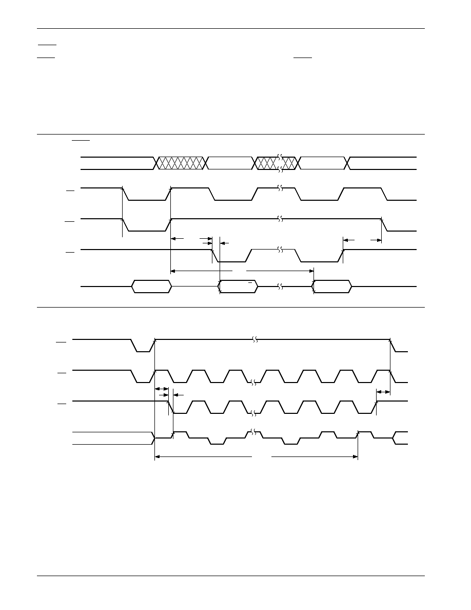
WE
CE
OE
I/O6
tOEH
tOE
tOES
tWC
(1)
(1)
ADDRESS
CE
WE
OE
I/O7
DIN = X
DOUT = X
DOUT = X
tOE
tOEH
tWC
tOES
DATA Polling
DATA polling is provided to indicate the completion of
write cycle. Once a byte write or page write cycle is
initiated, attempting to read the last byte written will
output the complement of that data on I/O
7
(I/O
0
I/O
6
are indeterminate) until the programming cycle is
complete. Upon completion of the self-timed write cycle,
all I/O's will output true data during a read cycle.
Toggle Bit
In addition to the DATA Polling feature of the CAT28C257,
the device offers an additional method for determining
the completion of a write cycle. While a write cycle is in
progress, reading data from the device will result in I/O
6
toggling between one and zero. However, once the write
is complete, I/O
6
stops toggling and valid data can be
read from the device.
Figure 7. DATA Polling
28C257 F10
Figure 8. Toggle Bit
28C257 F11
Note:
(1)
Beginning and ending state of I/O
6
is indeterminate.
CAT28C257
9
Doc. No. 1015, Rev. B
Note:
(1)
Write protection is activated at this point whether or not any more writes are completed. Writing to addresses must occur within t
BLC
Max., after SDP activation.
HARDWARE DATA PROTECTION
The following is a list of hardware data protection features
that are incorporated into the CAT28C257.
(1) V
CC
sense provides for write protection when V
CC
falls below 3.5V min.
(2) A power on delay mechanism, t
INIT
(see AC
characteristics), provides a 5 to 10 ms delay before
a write sequence, after V
CC
has reached 3.5V min.
(3) Write inhibit is activated by holding any one of
OE
low,
CE
high or
WE
high.
(4) Noise pulses of less than 20 ns on the
WE
or
CE
inputs will not result in a write cycle.
SOFTWARE DATA PROTECTION
The CAT28C257 features a software controlled data
protection scheme which, once enabled, requires a data
algorithm to be issued to the device before a write can be
performed. The device is shipped from Catalyst with the
software protection NOT ENABLED (the CAT28C257 is
in the standard operating mode).
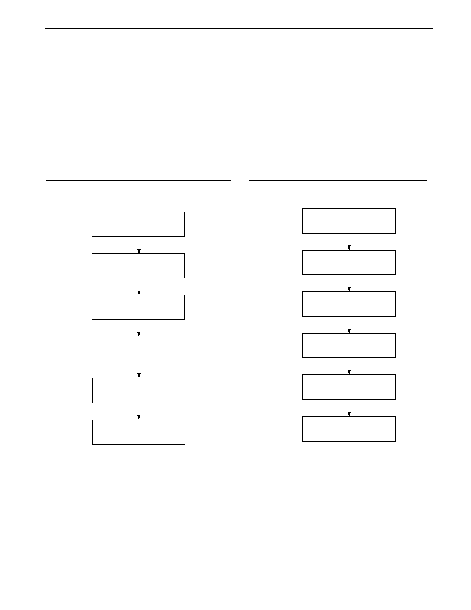
Figure 9. Write Sequence for Activating Software
Data Protection
Figure 10. Write Sequence for Deactivating
Software Data Protection
5096 FHD F08
5096 FHD F09
SOFTWARE DATA
PROTECTION ACTIVATED
(12)
WRITE DATA:
XX
WRITE LAST BYTE
TO
LAST ADDRESS
TO ANY ADDRESS
WRITE DATA:
AA
ADDRESS:
5555
WRITE DATA:
55
ADDRESS:
2AAA
WRITE DATA:
A0
ADDRESS:
5555
(1)
WRITE DATA:
AA
ADDRESS:
5555
WRITE DATA:
55
ADDRESS:
2AAA
WRITE DATA:
80
ADDRESS:
5555
WRITE DATA:
AA
ADDRESS:
5555
WRITE DATA:
55
ADDRESS:
2AAA
W R I T E DATA :
20
ADDRESS:
5555
CAT28C257
10
Doc. No. 1015, Rev. B
To activate the software data protection, the device must
be sent three write commands to specific addresses with
specific data (Figure 9). This sequence of commands
(along with subsequent writes) must adhere to the page
write timing specifications (Figure 11). Once this is done,
all subsequent byte or page writes to the device must be
preceded by this same set of write commands. The data
protection mechanism is activated until a deactivate
sequence is issued regardless of power on/off transitions.
This gives the user added inadvertent write protection
on power-up in addition to the hardware protection
provided.
To allow the user the ability to program the device with
an E
2
PROM programmer (or for testing purposes) there
is a software command sequence for deactivating the
data protection. The six step algorithm (Figure 10) will
reset the internal protection circuitry, and the device will
return to standard operating mode (Figure 12 provides
reset timing). After the sixth byte of this reset sequence
has been issued, standard byte or page writing can
commence.
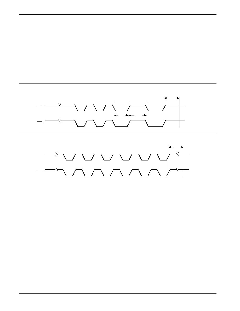
Figure 11. Software Data Protection Timing
5096 FHD F13
CE
WE
tWP
AA
5555
55
2AAA
A0
5555
DATA
ADDRESS
tBLC
tWC
BYTE OR
PAGE
WRITES
ENABLED
Figure 12. Resetting Software Data Protection Timing
CE
WE
AA
5555
55
2AAA
DATA
ADDRESS
tWC
80
5555
AA
5555
55
2AAA
20
5555
SDP
RESET
DEVICE
UNPROTECTED
5096 FHD F14
CAT28C257
11
Doc. No. 1015, Rev. B
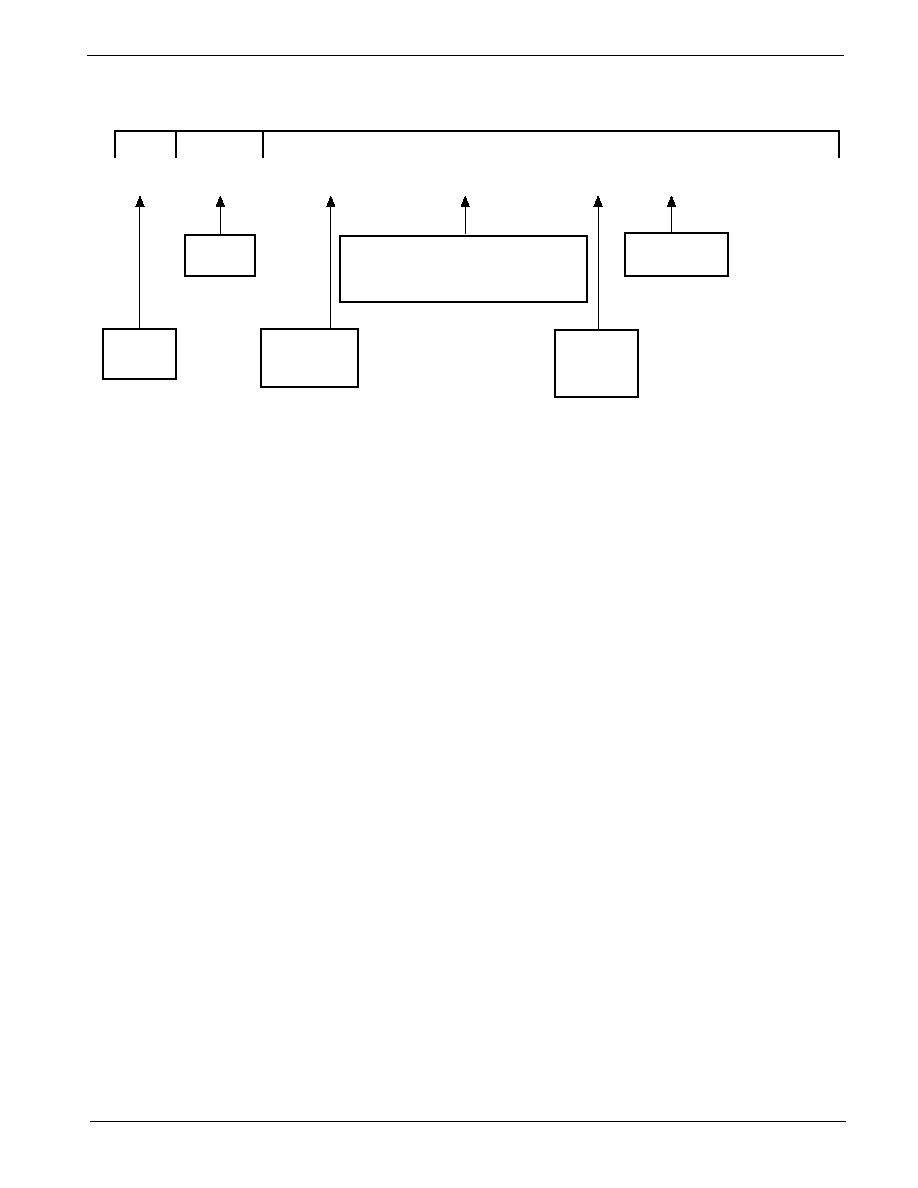
ORDERING INFORMATION
Notes:
(1)
The device used in the above example is a CAT28C257NI-90T (100,000 Cycle Endurance, PLCC, Industrial temperature, 200 ns
Access Time, Tape & Reel).
28C257 F17a
Speed
12: 120ns
15: 150ns
Prefix
Device #
Suffix
28C257
Product
Number
CAT
Optional
Company
ID
N
I
T
Tape & Reel
T: 500/Reel
Package
P: PDIP
N: PLCC
-90
Temperature Range
Blank = Commercial (0°C to +70°C)
I = Industrial (-40°C to +85°C)
A = Automotive (-40° to +105°C)*
* -40°C to +125°C is available upon request

Catalyst Semiconductor, Inc.
Corporate Headquarters
1250 Borregas Avenue
Sunnyvale, CA 94089
Phone: 408.542.1000
Fax: 408.542.1200
www.catalyst-semiconductor.com
Copyrights, Trademarks and Patents
Trademarks and registered trademarks of Catalyst Semiconductor include each of the following:
DPP TM
AE
2
TM
Catalyst Semiconductor has been issued U.S. and foreign patents and has patent applications pending that protect its products. For a complete list of patents
issued to Catalyst Semiconductor contact the Company's corporate office at 408.542.1000.
CATALYST SEMICONDUCTOR MAKES NO WARRANTY, REPRESENTATION OR GUARANTEE, EXPRESS OR IMPLIED, REGARDING THE SUITABILITY OF ITS
PRODUCTS FOR ANY PARTICULAR PURPOSE, NOR THAT THE USE OF ITS PRODUCTS WILL NOT INFRINGE ITS INTELLECTUAL PROPERTY RIGHTS OR THE
RIGHTS OF THIRD PARTIES WITH RESPECT TO ANY PARTICULAR USE OR APPLICATION AND SPECIFICALLY DISCLAIMS ANY AND ALL LIABILITY ARISING
OUT OF ANY SUCH USE OR APPLICATION, INCLUDING BUT NOT LIMITED TO, CONSEQUENTIAL OR INCIDENTAL DAMAGES.
Catalyst Semiconductor products are not designed, intended, or authorized for use as components in systems intended for surgical implant into the body, or
other applications intended to support or sustain life, or for any other application in which the failure of the Catalyst Semiconductor product could create a
situation where personal injury or death may occur.
Catalyst Semiconductor reserves the right to make changes to or discontinue any product or service described herein without notice. Products with data sheets
labeled "Advance Information" or "Preliminary" and other products described herein may not be in production or offered for sale.
Catalyst Semiconductor advises customers to obtain the current version of the relevant product information before placing orders. Circuit diagrams illustrate
typical semiconductor applications and may not be complete.
Publication #:
1015
Revison:
B
Issue date:
5/2/02
Type:
Final