
Caution Observe precautions when handling because these devices are sensitive to electrostatic discharge.
HETERO JUNCTION FIELD EFFECT TRANSISTOR
NE3512S02
C TO Ku BAND SUPER LOW NOISE AMPLIFIER
N-CHANNEL HJ-FET
FEATURES
∑ Super low noise figure and high associated gain
NF = 0.35 dB TYP., G
a
= 13.5 dB TYP. @ f = 12 GHz
∑ Micro-X plastic (S02) package
APPLICATIONS
∑ C to Ku-band DBS LNB
∑ Other C to Ku-band communication systems
ORDERING INFORMATION
Part Number
Order Number
Package
Quantity
Marking
Supplying Form
NE3512S02-T1C NE3512S02-T1C-A
2
kpcs/reel
C
NE3512S02-T1D NE3512S02-T1D-A
S02 (Pb-Free)
10 kpcs/reel
∑ 8 mm wide embossed taping
∑ Pin 4 (Gate) faces the perforation side
of the tape
Remark To order evaluation samples, contact your nearby sales office.
Part number for sample order: NE3512S02
ABSOLUTE MAXIMUM RATINGS (T
A
= +25
∞
C)
Parameter Symbol
Ratings Unit
Drain to Source Voltage
V
DS
4 V
Gate to Source Voltage
V
GS
-
3 V
Drain Current
I
D
I
DSS
mA
Gate Current
I
G
100
µ
A
Total Power Dissipation
P
tot
Note
165 mW
Channel Temperature
T
ch
+125
∞
C
Storage Temperature
T
stg
-
65 to +125
∞
C
Note Mounted on 1.08 cm
2
◊
1.0 mm (t) glass epoxy PCB
Document No. PG10592EJ01V0DS (1st edition)
Date Published February 2006 CP(N)

NE3512S02
RECOMMENDED OPERATING CONDITIONS (T
A
= +25
∞
C)
Parameter Symbol
MIN.
TYP.
MAX.
Unit
Drain to Source Voltage
V
DS
1 2 3 V
Drain Current
I
D
5 10 15
mA
Input Power
P
in
-
-
0 dBm
ELECTRICAL CHARACTERISTICS (T
A
= +25
∞
C, unless otherwise specified)
Parameter Symbol
Test
Conditions MIN.
TYP.
MAX.
Unit
Gate to Source Leak Current
I
GSO
V
GS
=
-
3 V
-
0.5 10
µ
A
Saturated Drain Current
I
DSS
V
DS
= 2 V, V
GS
= 0 V
15
40
70
mA
Gate to Source Cutoff Voltage
V
GS (off)
V
DS
= 2 V, I
D
= 100
µ
A
-
0.2
-
0.7
-
2.0 V
Transconductance g
m
V
DS
= 2 V, I
D
= 10 mA
40
55
-
mS
Noise Figure
NF
V
DS
= 2 V, I
D
= 10 mA, f = 12 GHz
-
0.35 0.5 dB
Associated Gain
G
a
12.5 13.5
-
dB
Data Sheet PG10592EJ01V0DS
2
NE3512S02
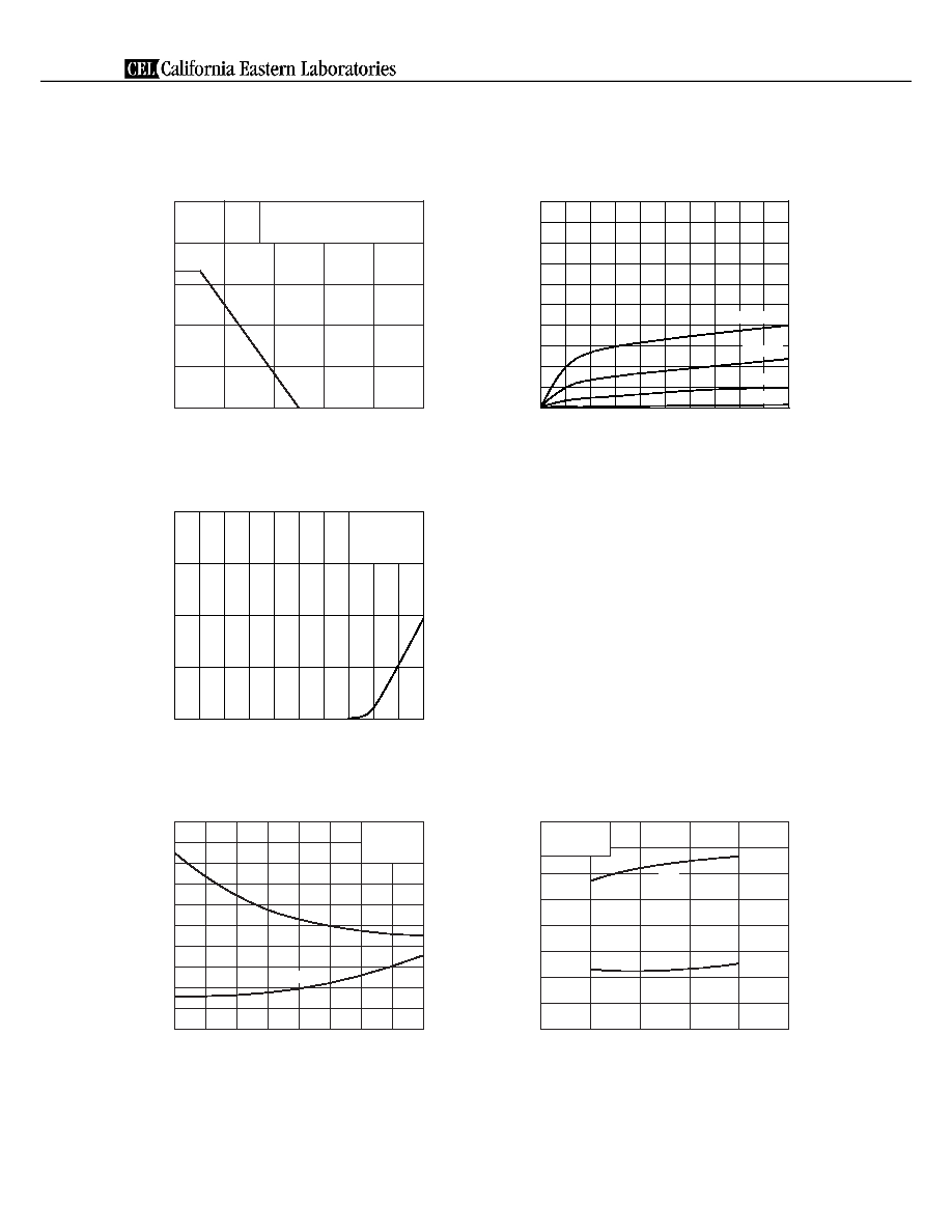
TYPICAL CHARACTERISTICS (T
A
= +25
∞
C, unless otherwise specified)
Total Power Dissipation P
tot
(mW)
Ambient Temperature T
A
(∞C)
vs. AMBIENT TEMPERATURE
TOTAL POWER DISSIPATION
250
200
150
100
50
0
50
100
150
200
250
80
60
40
20
0
≠2.0
≠1.0
0
Drain Current I
D
(mA)
Gate to Source Voltage V
GS
(V)
DRAIN CURRENT vs.
GATE TO SOURCE VOLTAGE
V
DS
= 2 V
Drain Current I
D
(mA)
Minimum Noise Figure NF
min
(dB)
Associated Gain G
a
(dB)
ASSOCIATED GAIN vs. DRAIN CURRENT
MINIMUM NOISE FIGURE,
f = 12 GHz
V
DS
= 2 V
NF
min
G
a
V
DS
= 2 V
I
D
= 10 mA
NF
min
Drain Current I
D
(mA)
Drain to Source Voltage V
DS
(V)
DRAIN TO SOURCE VOLTAGE
DRAIN CURRENT vs.
100
20
40
60
80
0
1.0
2.0
V
GS
= 0 V
≠
0.2 V
≠
0.4 V
≠
0.6 V
Mounted on Glass Epoxy PCB
(1.08 cm
2
◊
1.0 mm (t) )
Frequency f (GHz)
Minimum Noise Figure NF
min
(dB)
Associated Gain G
a
(dB)
ASSOCIATED GAIN vs. FREQUENCY
MINIMUM NOISE FIGURE,
2.0
1.2
1.4
1.6
1.8
0.6
0.8
1.0
0.2
0.4
0.0
10
15
0
5
20
25
1.2
1.4
1.6
0.6
0.8
1.0
0.2
0.4
0.0
12
14
16
6
8
10
2
4
0
25
15
10
5
20
0
8
6
2
4
14
12
10
16
18
G
a
Remark The graphs indicate nominal characteristics.
Data Sheet PG10592EJ01V0DS
3

NE3512S02
S-PARAMETERS
S-parameters/Noise parameters are provided on the NEC Compound Semiconductor Devices Web site in a form
(S2P) that enables direct import to a microwave circuit simulator without keyboard input.
Click here to download S-parameters.
[RF and Microwave]
[Device Parameters]
URL http://www.ncsd.necel.com/
Data Sheet PG10592EJ01V0DS
4
NE3512S02
RF MEASURING LAYOUT PATTERN (REFERENCE ONLY) (UNIT: mm)
13.0
2.80
L2≠uX Ver. 1
1.7 mm/R.P.
2.60
2.06
2.6
1.7
1.7
Reference Plane
(Calibration Plane)
Reference Plane
(Calibration Plane)
6.0
0.64
0.74
2.06
0.54
0.3 TH
RT/duroid 5880/ROGERS
t = 0.254 mm
r = 2.20
tan delta = 0.0009 @10 GHz
Data Sheet PG10592EJ01V0DS
5

NE3512S02
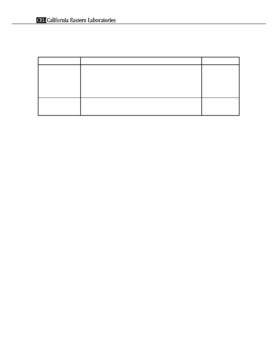
PACKAGE DIMENSIONS
S02 (UNIT: mm)
PIN CONNECTIONS
1. Source
2. Drain
3. Source
4. Gate
(Top View)
(Side View)
(Bottom View)
0.5 TYP.
2.6±0.1
0.65 TYP.
3.2±0.2
C
1
2
3
4
2.2±0.2
3.2±0.2
1.7
1.5 MAX.
0.15±0.05
3
4
1
2
2.2±0.2
2.2±0.2
Data Sheet PG10592EJ01V0DS
6
NE3512S02
RECOMMENDED SOLDERING CONDITIONS
This product should be soldered and mounted under the following recommended conditions. For soldering
methods and conditions other than those recommended below, contact your nearby sales office.
Soldering Method
Soldering Conditions Condition
Symbol
Infrared Reflow
Peak temperature (package surface temperature)
: 260
∞
C or below
Time at peak temperature
: 10 seconds or less
Time at temperature of 220
∞
C or higher
: 60 seconds or less
Preheating time at 120 to 180
∞
C :
120
±
30 seconds
Maximum number of reflow processes
: 3 times
Maximum chlorine content of rosin flux (% mass)
: 0.2%(Wt.) or below
IR260
Partial Heating
Peak temperature (terminal temperature)
: 350
∞
C or below
Soldering time (per side of device)
: 3 seconds or less
Maximum chlorine content of rosin flux (% mass)
: 0.2%(Wt.) or below
HS350
Caution Do not use different soldering methods together (except for partial heating).
Data Sheet PG10592EJ01V0DS
7
4590 Patrick Henry Drive
Santa Clara, CA 95054-1817
Telephone: (408) 919-2500
Facsimile: (408) 988-0279
Subject: Compliance with EU Directives
CEL certifies, to its knowledge, that semiconductor and laser products detailed below are compliant
with the requirements of European Union (EU) Directive 2002/95/EC Restriction on Use of Hazardous
Substances in electrical and electronic equipment (RoHS) and the requirements of EU Directive
2003/11/EC Restriction on Penta and Octa BDE.
CEL Pb-free products have the same base part number with a suffix added. The suffix ≠A indicates
that the device is Pb-free. The ≠AZ suffix is used to designate devices containing Pb which are
exempted from the requirement of RoHS directive (*). In all cases the devices have Pb-free terminals.
All devices with these suffixes meet the requirements of the RoHS directive.
This status is based on CEL's understanding of the EU Directives and knowledge of the materials that
go into its products as of the date of disclosure of this information.
Restricted Substance
per RoHS
Concentration Limit per RoHS
(values are not yet fixed)
Concentration contained
in CEL devices
-A -AZ
Lead (Pb)
< 1000 PPM
Not Detected
(*)
Mercury
< 1000 PPM
Not Detected
Cadmium
< 100 PPM
Not Detected
Hexavalent Chromium
< 1000 PPM
Not Detected
PBB
< 1000 PPM
Not Detected
PBDE
< 1000 PPM
Not Detected
If you should have any additional questions regarding our devices and compliance to environmental
standards, please do not hesitate to contact your local representative.
Important Information and Disclaimer: Information provided by CEL on its website or in other communications concerting the substance
content of its products represents knowledge and belief as of the date that it is provided. CEL bases its knowledge and belief on information
provided by third parties and makes no representation or warranty as to the accuracy of such information. Efforts are underway to better
integrate information from third parties. CEL has taken and continues to take reasonable steps to provide representative and accurate
information but may not have conducted destructive testing or chemical analysis on incoming materials and chemicals. CEL and CEL
suppliers consider certain information to be proprietary, and thus CAS numbers and other limited information may not be available for
release.
In no event shall CEL's liability arising out of such information exceed the total purchase price of the CEL part(s) at issue sold by CEL to
customer on an annual basis.
See CEL Terms and Conditions for additional clarification of warranties and liability.