
PART NUMBER
NE687M13
EIAJ
1
REGISTERED NUMBER
2SC5618
PACKAGE OUTLINE
M13
SYMBOLS
PARAMETERS AND CONDITIONS
UNITS
MIN
TYP
MAX
f
T
Gain Bandwidth at V
CE
= 2 V, I
C
= 20 mA, f = 2 GHz
GHz
9.0
14.0
V
CE
= 1 V, I
C
= 10 mA, f = 2 GHz
GHz
7.0
12.0
NF
Noise Figure at V
CE
= 2 V, I
C
= 3 mA, f = 2 GHz, Z
s
= Z
opt
dB
1.4
2.0
V
CE
= 1 V, I
C
= 3 mA, f = 2 GHz, Z
s
= Z
opt
dB
1.5
2.0
|S
21E
|
2
Insertion Power Gain at V
CE
= 2 V, I
C
= 20 mA, f = 2 GHz
dB
8.5
10.0
V
CE
= 1 V, I
C
= 10 mA, f = 2 GHz
dB
6.0
9.0
h
FE
Forward Current Gain at V
CE
= 2 V, I
C
= 20 mA,
Note 2
70
130
I
CBO
Collector Cutoff Current at V
CB
= 5 V, I
E
= 0
µA
0.1
I
EBO
Emitter Cutoff Current at V
EB
= 1 V, I
C
= 0
µA
0.1
C
RE
Feedback Capacitance at V
CB
= 2 V, I
E
= 0, f = 1 MHz,
Note 3
pF
0.4
0.8
NE687M13
NEC's NPN SILICON TRANSISTOR
∑
NEW MINIATURE M13 PACKAGE:
≠ Small transistor outline
≠ 1.0 X 0.5 X 0.5 mm
≠ Low profile / 0.50 mm package height
≠ Flat lead style for better RF performance
∑
HIGH GAIN BANDWIDTH PRODUCT:
f
T
= 14 GHz
∑
LOW NOISE FIGURE:
NF = 1.4 dB at 2 GHz
FEATURES
OUTLINE DIMENSIONS
(Units in mm)
PACKAGE OUTLINE M13
ELECTRICAL CHARACTERISTICS
(T
A
= 25∞C)
California Eastern Laboratories
Notes:
1. Electronic Industrial Association of Japan.
2. Pulsed measurement, pulse width 350 µs, duty cycle 2 %.
3. Capacitance is measured with emitter and case connected to the guard terminal of the bridge.
DESCRIPTION
NEC's NE687M13 transistor is designed for low noise, high
gain, and low cost requirements. This high f
T
part is well suited
for very low voltage/low current designs for portable wireless
communications and cellular radio applications. NEC's new
low profile/flat lead style "M13" package is ideal for today's
portable wireless applications.
1. Emitter
2. Base
3. Collector
PIN CONNECTIONS
0.125
+0.1 Ò0.05
0.5±0.05
0.1
0.1
0.2
+0.1 Ò0.05
0.35
0.7
0.35
0.15
+0.1 Ò0.05
0.15
+0.1 Ò0.05
1.0
+0.1 Ò0.05
0.5
+0.1
Ò0.05
0.7±0.05
1
2
3
W2
0.3
0.2
0.2
(Bottom View)

Notes:
1. Operation in excess of any one of these parameters may result
in permanent damage.
2. With device mounted on 1.08 cm
2
X 1.2 mm glass epoxy board.
SYMBOLS
PARAMETERS
UNITS
RATINGS
V
CBO
Collector to Base Voltage
V
5.0
V
CEO
Collector to Emitter Voltage
V
3.0
V
EBO
Emitter to Base Voltage
V
2.0
I
C
Collector Current
mA
30
P
T
Total Power Dissipation
2
mW
90
T
J
Junction Temperature
∞C
150
T
STG
Storage Temperature
∞C
-65 to +150
ABSOLUTE MAXIMUM RATINGS
1
(T
A
= 25∞C)
TYPICAL PERFORMANCE CURVES
(T
A
= 25∞C)
Ambient Temperature, T
A
(∞C)
Total Power Dissipation, P
tot
(mW)
TOTAL POWER DISSIPATION vs.
AMBIENT TEMPERATURE
Collector to Base Voltage, V
CB
(V)
Reverse Transfer Capacitance, C
re
(pF)
REVERSE TRANSFR CAPACITANCE vs.
COLLECTOR TO BASE VOLTAGE
Mounted on Glass Epoxy PCB
(1.08 cm
2
◊ 1.0 mm (t) )
300
250
200
150
90
100
50
0
25
50
75
100
125
150
f = 1 MHz
0.6
0.5
0.4
0.3
0.2
0.1
0
1
2
3
4
5
35
30
25
20
15
10
5
0
1
2
3
4
100 A
µ
200 A
µ
400 A
µ
500 A
µ
300 A
µ
I
B
: 50 A step
µ
I
B
= 50 A
µ
NE687M13
Base to Emmiter Voltage, V
BE
(V)
Collector Current, I
C
(mA)
COLLECTOR CURRENT vs.
BASE TO EMITTER VOLTAGE
V
CE
= 2 V
100
10
1
0.01
0.001
0.1
0.0001
0.7
0.5
0.6
0.4
0.8
0.9
1.0
Collector to Emmiter Voltage, V
CE
(V)
Collector Current, I
C
(mA)
COLLECTOR CURRENT vs.
COLLECTOR TO EMITTER VOLTAGE
PART NUMBER
QUANTITY
NE687M13-A
NE687M13-T3-A
ORDERING INFORMATION

TYPICAL PERFORMANCE CURVES
(T
A
= 25∞C)
Collector Current, I
C
(mA)
DC Current Gain, H
FE
DC CURRENT GAIN
vs. COLLECTOR CURRENT
NE687M13
Collector Current, I
C
(mA)
Gain Bandwidth Product, f
T
(GHz)
GAIN BANDWIDTH PRODUCT
vs. COLLECTOR CURRENT
Frequency, f (GHz)
Insertion Power Gain, |S
21e
|
2
(dB)
Maximum Available Gain, MAG(dB)
Maximum Stable Gain, MSG(dB)
INSERTION POWER GAIN,
MAG, MSG vs. FREQUENCY
Collector Current, I
C
(mA)
Insertion Power Gain, |S
21e
|
2
(dB)
Maximum Available Gain, MAG(dB)
Maximum Stable Gain, MSG(dB)
INSERTION POWER GAIN, MAG, MSG
vs. COLLECTOR CURRENT
V
CE
= 2 V
1000
100
10
1
10
0.1
100
V
CE
= 2 V
f = 2 GHz
16
14
12
10
8
6
4
2
0
10
1
100
V
CE
= 1 V
I
C
= 10 mA
35
30
25
20
15
10
5
0
0.1
1
10
MAG
MSG
|S
21e
|
2
V
CE
= 2 V
I
C
= 10 mA
35
30
25
20
15
10
5
0
0.1
1
10
MAG
MSG
|S
21e
|
2
V
CE
= 2 V
f = 1 GHz
20
15
10
5
0
1
10
100
MAG
MSG
|S
21e
|
2
V
CE
= 2 V
f = 2 GHz
20
15
10
5
0
1
10
100
MAG
MSG
|S
21e
|
2

TYPICAL PERFORMANCE CURVES
(T
A
= 25∞C)
Collector Current, I
C
(mA)
Noise Figure, NF (dB)
NOISE FIGURE, ASSOCIATED GAIN
vs. COLLECTOR CURRENT
NE687M13
Collector Current, I
C
(mA)
Noise Figure, NF (dB)
NOISE FIGURE, ASSOCIATED GAIN
vs. COLLECTOR CURRENT
Collector Current, I
C
(mA)
Noise Figure, NF (dB)
NOISE FIGURE, ASSOCIATED GAIN
vs. COLLECTOR CURRENT
Collector Current, I
C
(mA)
Noise Figure, NF (dB)
NOISE FIGURE, ASSOCIATED GAIN
vs. COLLECTOR CURRENT
Collector Current, I
C
(mA)
Noise Figure, NF (dB)
NOISE FIGURE, ASSOCIATED GAIN
vs. COLLECTOR CURRENT
Collector Current, I
C
(mA)
Noise Figure, NF (dB)
NOISE FIGURE, ASSOCIATED GAIN
vs. COLLECTOR CURRENT
5
4
3
2
1
0
20
16
12
8
4
0
1
10
100
V
CE
= 1 V
f = 1 GHz
G
a
NF
5
4
3
2
1
0
20
16
12
8
4
0
1
10
100
V
CE = 2 V
f = 1 GHz
G
a
NF
5
4
3
2
1
0
20
16
12
8
4
0
1
10
100
V
CE
= 1 V
f = 1.5 GHz
G
a
NF
5
4
3
2
1
0
20
16
12
8
4
0
1
10
100
V
CE
= 2 V
f = 1.5 GHz
G
a
NF
5
4
3
2
1
0
20
16
12
8
4
0
1
10
100
V
CE
= 1 V
f = 2 GHz
G
a
NF
5
4
3
2
1
0
20
16
12
8
4
0
1
10
100
V
CE
= 2 V
f = 2 GHz
G
a
NF
Associated Gain, G
a
(dB)
Associated Gain, G
a
(dB)
Associated Gain, G
a
(dB)
Associated Gain, G
a
(dB)
Associated Gain, G
a
(dB)
Associated Gain, G
a
(dB)
NE687M13
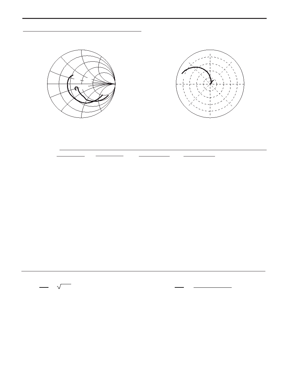
TYPICAL SCATTERING PARAMETERS
NE687M13
V
CE
= 1 V, I
C
= 10 mA
Frequency
S
11
S
21
S
12
S
22
K
MAG
1
GHz
MAG
ANG
MAG
ANG
MAG
ANG
MAG
ANG
(dB)
0.100
0.71
-28.83
21.86
158.87
0.02
76.89
0.86
-22.59
0.19
29.94
0.200
0.64
-56.70
19.01
141.86
0.04
64.05
0.75
-40.78
0.28
27.02
0.300
0.57
-77.87
16.05
129.44
0.05
57.48
0.63
-54.59
0.37
25.16
0.400
0.53
-94.58
13.57
120.29
0.06
54.28
0.54
-64.96
0.46
23.79
0.500
0.49
-107.39
11.62
113.50
0.06
52.33
0.47
-72.99
0.54
22.68
0.600
0.45
-120.85
9.91
108.06
0.07
51.39
0.37
-78.86
0.68
21.71
0.700
0.44
-129.42
8.73
103.77
0.07
51.70
0.33
-85.54
0.74
20.83
0.800
0.44
-135.99
7.80
100.31
0.08
52.15
0.30
-90.17
0.79
20.04
0.900
0.43
-141.83
7.02
97.30
0.08
52.52
0.28
-94.31
0.83
19.34
1.000
0.43
-146.64
6.38
94.61
0.09
53.11
0.26
-99.34
0.88
18.67
1.200
0.42
-153.87
5.40
90.05
0.10
54.26
0.23
-106.29
0.94
17.49
1.400
0.42
-160.59
4.69
86.18
0.11
55.29
0.21
-113.29
0.99
16.45
1.600
0.42
-165.22
4.14
82.82
0.12
56.05
0.19
-118.74
1.03
14.43
1.800
0.42
-169.18
3.71
79.73
0.13
56.51
0.18
-123.68
1.06
13.15
2.000
0.41
-172.49
3.37
76.86
0.14
56.83
0.17
-128.17
1.08
12.13
2.500
0.40
179.29
2.76
70.23
0.16
56.91
0.16
-136.91
1.12
10.14
3.000
0.40
171.08
2.35
64.05
0.19
55.87
0.17
-143.47
1.14
8.61
3.500
0.39
161.33
2.05
58.49
0.21
54.71
0.18
-147.06
1.16
7.38
4.000
0.40
152.78
1.83
53.56
0.24
53.37
0.20
-147.25
1.16
6.41
4.500
0.39
146.02
1.66
49.23
0.26
52.04
0.22
-144.73
1.16
5.60
5.000
0.38
141.59
1.53
45.35
0.29
50.81
0.23
-140.61
1.15
4.94
5.500
0.36
138.25
1.44
41.63
0.31
49.38
0.23
-135.48
1.14
4.40
6.000
0.34
134.43
1.36
37.72
0.34
47.54
0.23
-133.06
1.13
3.90
Coordinates in Ohms
Frequency in GHz
V
CE
= 1 V, I
C
= 10 mA
MAG =
|S
21
|
|S
12
|
K - 1
).
2
(
K ±
= S
11
S
22
- S
21
S
12
When K 1, MAG is undefined and MSG values are used. MSG =
|S
21
|
|S
12
|
, K = 1 + | | - |S
11
| - |S
22
|
2
2
2
2 |S
12
S
21
|
,
Note:
1. Gain Calculations:
MAG = Maximum Available Gain
MSG = Maximum Stable Gain
j50
j100
j25
j10
0
-j10
-j25
-j50
-j100
10
50
100
25
S22
S11
+90∫
+45∫
+0∫
+0∫
5 10 15 20 25
-45∫
-90∫
-135∫
+180∫
+135∫
S12
S21