NE851M03
NE851M03
NEC's NPN SILICON TRANSISTOR
·
NEW MINIATURE M03 PACKAGE:
Small transistor outline
Low profile / 0.59 mm package height
Flat lead style for better RF performance
·
IDEAL FOR
3 GHz OSCILLATORS
·
LOW 1/f NOISE
·
LOW PUSHING FACTOR
FEATURES
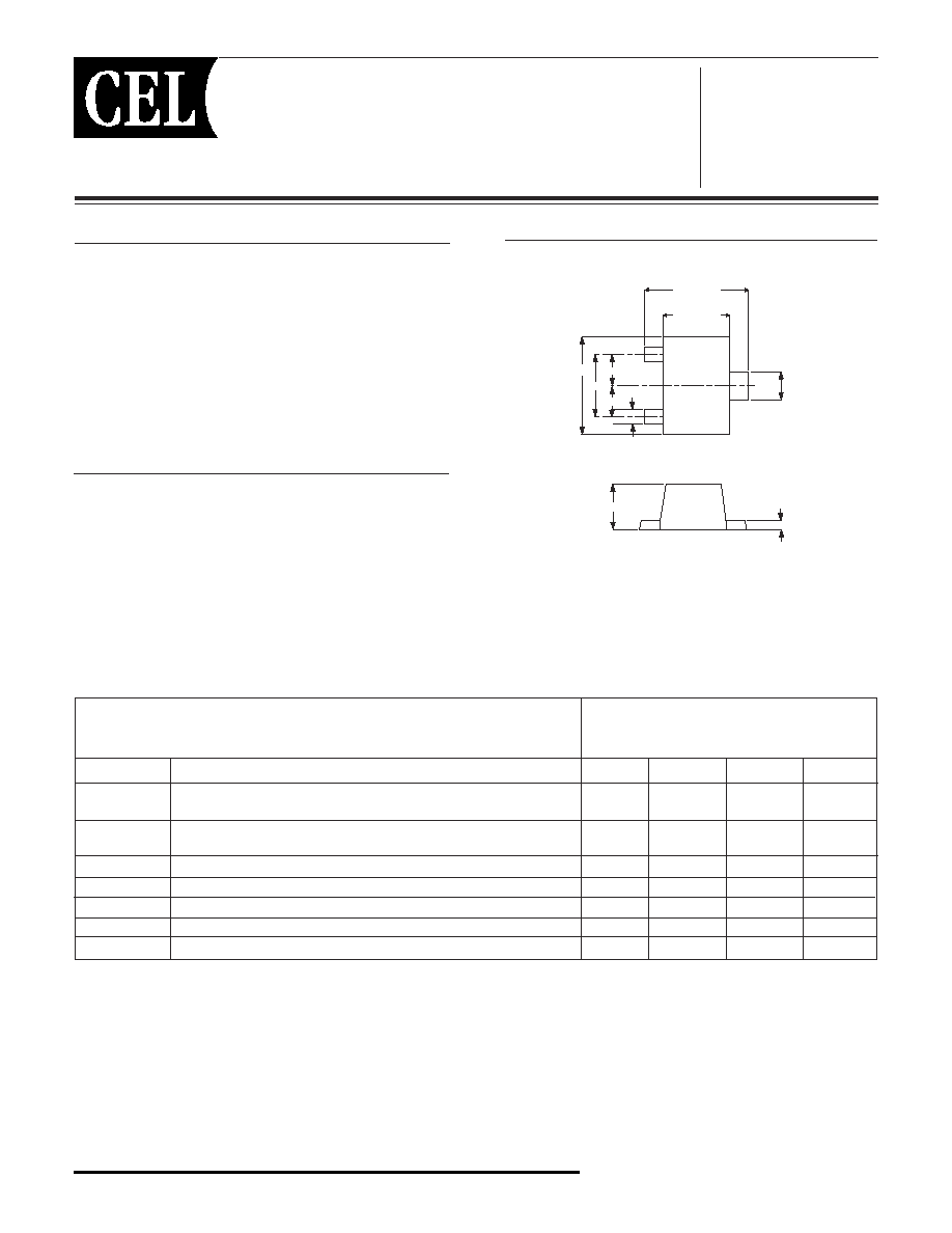
OUTLINE DIMENSIONS
(Units in mm)
PACKAGE OUTLINE M03
PART NUMBER
NE851M03
EIAJ
1
REGISTERED NUMBER
2SC5800
PACKAGE OUTLINE
M03
SYMBOLS
PARAMETERS AND CONDITIONS
UNITS
MIN
TYP
MAX
f
T
Gain Bandwidth at V
CE
= 1 V, I
C
= 5 mA, f = 2 GHz
GHz
3.0
4.5
f
T
Gain Bandwidth
at V
CE
= 1 V, I
C
= 15 mA, f = 2 GHz
GHz
5.0
6.5
|S
21E
|
2
Insertion Power Gain at V
CE
= 1 V, I
C
= 5 mA, f = 2 GHz
dB
3.0
4.0
|S
21E
|
2
Insertion Power Gain
at V
CE
= 1 V, I
C
= 15 mA, f = 2 GHz
dB
4.5
5.5
NF
Noise Figure at V
CE
= 1 V, I
C
= 10 mA, f = 2 GHz, Zs = Z
opt
dB
1.9
2.5
C
RE
Reverse Transfer Capacitance
3
at V
CB
= 0.5 V, I
E
= 0 mA, f = 1 MHz
pF
0.6
0.8
I
CBO
Collector Cutoff Current at V
CB
= 5 V, I
E
= 0
nA
600
I
EBO
Emitter Cutoff Current at V
EB
= 1 V, I
C
= 0
nA
600
h
FE
DC Current Gain
2
at V
CE
= 1 V, I
C
= 5 mA
100
120
145
ELECTRICAL CHARACTERISTICS
(T
A
= 25
°
C)
Notes:
1. Electronic Industrial Association of Japan.
2. Pulsed measurement, pulse width
350
µ
s, duty cycle
2 %.
3. Collector to base capacitance when the emitter is grounded
DESCRIPTION
NEC's NE851M03 transistor is designed for oscillator applica-
tions up to 3 GHz. The NE851M03 features low voltage
operation, low phase noise, and high immunty to pushing
effects. NEC's low profile/flat lead style "M03" package is ideal
for today's portable wireless applications.
1
3
2
1.2±0.05
0.8±0.1
+0.1
-0.05
+0.1
-0
+0.1
-0
0.15
1.4 ±0.1
(0.9)
0.59±0.05
0.2
0.45
0.45
0.3
80
1. Emitter
2. Base
3. Collector
PIN CONNECTIONS
California Eastern Laboratories
Notes:
1. Operation in excess of any one of these parameters may result
in permanent damage.
2. With device mounted on 1.08 cm
2
X 1.0 mm (t) glass epoxy
board.
SYMBOLS
PARAMETERS
UNITS
RATINGS
V
CBO
Collector to Base Voltage
V
9.0
V
CEO
Collector to Emitter Voltage
V
5.5
V
EBO
Emitter to Base Voltage
V
1.5
I
C
Collector Current
mA
100
P
T2
Total Power Dissipation
mW
200
T
J
Junction Temperature
°
C
150
T
STG
Storage Temperature
°
C
-65 to +150
ABSOLUTE MAXIMUM RATINGS
1
(T
A
= 25
°
C)
Ambient Temperature, T
A
(
°
C)
Total Power Dissipation, P
tot
(mW)
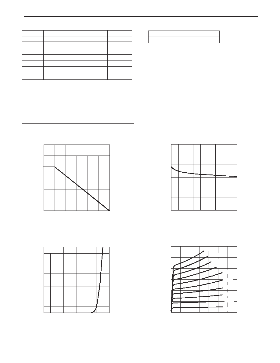
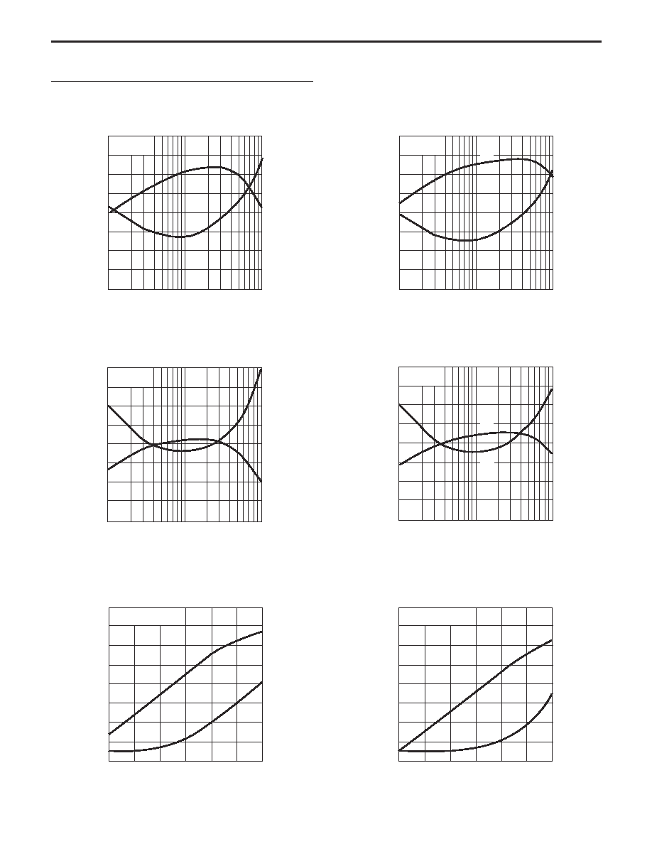
TOTAL POWER DISSIPATION vs.
AMBIENT TEMPERATURE
TYPICAL PERFORMANCE CURVES
(T
A
= 25
°
C)
Collector to Base Voltage, V
CB
(V)
Reverse Transfer Capacitance, C
re
(pF)
REVERSE TRANSFR CAPACITANCE vs.
COLLECTOR TO BASE VOLTAGE
NE851M03
Base to Emitter Voltage, V
BE
(V)
Collector Current, I
C
(mA)
COLLECTOR CURRENT vs.
BASE TO EMITTER VOLTAGE
PART NUMBER
QUANTITY
NE851M03-T3
3 k pcs./reel
ORDERING INFORMATION
Collector Current, I
C
(mA)
Collector to Emitter Voltage, V
CE
(V)
COLLECTOR CURRENT vs.
COLLECTOR TO EMITTER VOLTAGE
300
250
200
150
100
50
0
25
50
75
100
125
150
Mounted on Glass Epoxy PCB
(1.08 cm
2
x 1.0 mm(t) )
f = 1 MHz
1.0
0.8
0.6
0.4
0.2
0
1
2
3
4
5
6
7
8
9
V
CE
= 1 V
100
80
60
40
20
0
0.2
0.4
0.6
0.8
1.0
60
30
40
50
10
20
0
1
2
3
4
5
6
7
I
B
= 40 A
µ
320 A
µ
280 A
µ
240 A
µ
200 A
µ
160 A
µ
120 A
µ
80 A
µ
360 A
µ
400 A
µ
TYPICAL PERFORMANCE CURVES
(T
A
= 25
°
C)
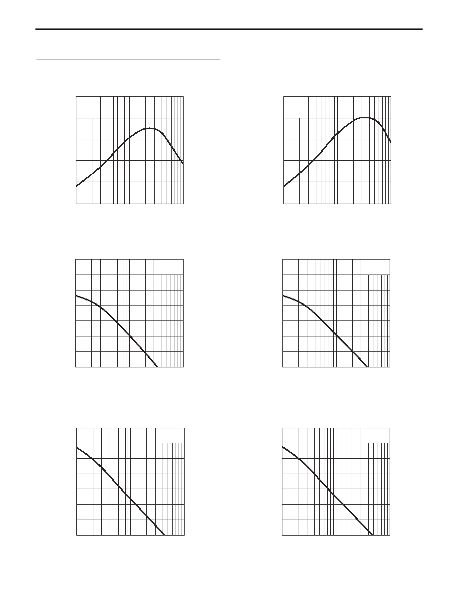
NE851M03
Collector Current, I
C
(mA)
Gain Bandwidth Product, f
T
(GHz)
GAIN BANDWIDTH PRODUCT
vs. COLLECTOR CURRENT
Gain Bandwidth Product, f
T
(GHz)
Collector Current, I
C
(mA)
GAIN BANDWIDTH PRODUCT
vs. COLLECTOR CURRENT
Frequency, f (GHz)
Insertion Power Gain, |S
21e
|
2
(dB)
INSERTION POWER GAIN vs.
FREQUENCY
Frequency, f (GHz)
Insertion Power Gain, |S
21e
|
2
(dB)
INSERTION POWER GAIN vs.
FREQUENCY
INSERTION POWER GAIN vs.
FREQUENCY
Frequency, f (GHz)
Insertion Power Gain, |S
21e
|
2
(dB)
INSERTION POWER GAIN vs.
FREQUENCY
Frequency, f (GHz)
Insertion Power Gain, |S
21e
|
2
(dB)
V
CE
= 1 V
f = 2 GHz
10
8
6
4
2
0
10
1
100
V
CE
= 2 V
f = 2 GHz
10
8
6
4
2
0
10
1
100
V
CE
= 1 V
I
C
= 5 mA
35
20
25
30
5
10
15
0
0.1
1
10
V
CE
= 2 V
I
C
= 5 mA
35
20
25
30
5
10
15
0
0.1
1
10
V
CE
= 1 V
I
C
= 15 mA
35
20
25
30
5
10
15
0
0.1
1
10
V
CE
= 2 V
I
C
= 15 mA
35
20
25
30
5
10
15
0
0.1
1
10
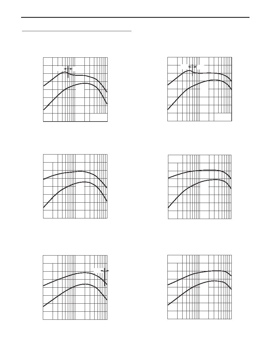
NE851M03
TYPICAL PERFORMANCE CURVES
(T
A
= 25
°
C)
Collector Current, I
C
(mA)
Insertion Power Gain, |S
21e
|
2
(dB)
Maximum Available Gain, MAG(dB)
Maximum Stable Gain, MSG(dB)
INSERTION POWER GAIN, MAG,
MSG vs. COLLECTOR CURRENT
Collector Current, I
C
(mA)
Insertion Power Gain, |S
21e
|
2
(dB)
Maximum Available Gain, MAG(dB)
Maximum Stable Gain, MSG(dB)
INSERTION POWER GAIN, MAG, MSG
vs. COLLECTOR CURRENT
Collector Current, I
C
(mA)
Insertion Power Gain, |S
21e
|
2
(dB)
Maximum Available Gain, MAG(dB)
INSERTION POWER GAIN and MAG
vs. COLLECTOR CURRENT
Collector Current, I
C
(mA)
Insertion Power Gain, |S
21e
|
2
(dB)
Maximum Available Gain, MAG(dB)
INSERTION POWER GAIN and MAG
vs. COLLECTOR CURRENT
Collector Current, I
C
(mA)
Insertion Power Gain, |S
21e
|
2
(dB)
Maximum Available Gain, MAG(dB)
Maximum Stable Gain, MSG(dB)
INSERTION POWER GAIN, MAG, MSG
vs. COLLECTOR CURRENT
Collector Current, I
C
(mA)
Insertion Power Gain, |S
21e
|
2
(dB)
Maximum Stable Gain, MSG(dB)
INSERTION POWER GAIN, MSG vs.
COLLECTOR CURRENT
V
CE
= 1 V
f = 1 GHz
20
15
5
10
0
1
10
100
MAG
MSG
|S
21e
|
2
V
CE
= 2 V
f = 1 GHz
20
15
5
10
0
1
10
100
MAG
MSG
|S
21e
|
2
V
CE
= 1 V
f = 2 GHz
15
10
0
5
-5
1
10
100
MAG
|S
21e
|
2
V
CE
= 2 V
f = 2 GHz
15
10
0
5
-5
1
10
100
MAG
|S
21e
|
2
V
CE
= 1 V
f = 4 GHz
10
5
-5
0
-10
1
10
100
MAG
MSG
|S
21e
|
2
V
CE
= 2 V
f = 4 GHz
10
5
-5
0
-10
1
10
100
MSG
|S
21e
|
2
TYPICAL PERFORMANCE CURVES
(T
A
= 25
°
C)
NE851M03
Collector Current, I
C
(mA)
Noise Figure, NF (dB)
NOISE FIGURE and ASSOCIATED GAIN
vs. COLLECTOR CURRENT
Associated Gain, G
a
(dB)
Noise Figure, NF (dB)
Collector Current, I
C
(mA)
NOISE FIGURE and ASSOCIATED GAIN
vs. COLLECTOR CURRENT
Associated Gain, G
a
(dB)
Collector Current, I
C
(mA)
Noise Figure, NF (dB)
NOISE FIGURE and ASSOCIATED GAIN
vs. COLLECTOR CURRENT
Associated Gain, G
a
(dB)
Noise Figure, NF (dB)
Collector Current, I
C
(mA)
NOISE FIGURE and ASSOCIATED GAIN
vs. COLLECTOR CURRENT
Associated Gain, G
a
(dB)
Input Power, P
IN
(dBm)
Output Power, P
OUT
(dBm)
OUTPUT POWER AND
COLLECTOR CURRENT vs.
INPUT POWER
Collector Current, I
C
(mA)
Input Power, P
IN
(dBm)
Output Power, P
OUT
(dBm)
OUTPUT POWER AND
COLLECTOR CURRENT vs.
INPUT POWER
Collector Current, I
C
(mA)
4
3
2
1
0
16
12
8
4
0
1
10
100
V
CE
= 1 V
f = 1 GHz
NF
G
a
4
3
2
1
0
16
12
8
4
0
1
10
100
V
CE
= 2 V
f = 1 GHz
NF
G
a
4
3
2
1
0
18
12
8
4
0
1
10
100
V
CE
= 1 V
f = 2 GHz
NF
G
a
4
3
2
1
0
18
12
8
4
0
1
10
100
V
CE
= 2 V
f = 2 GHz
NF
G
a
25
20
15
10
5
0
-5
-10
-15
-15
-10
-5
0
5
10
-20
80
70
60
50
40
P
out
I
C
30
20
10
0
V
CE
= 2 V, f = 1 GHz
I
Cq
= 5 mA (RF OFF)
25
20
15
10
5
0
-5
-10
-15
-15
-10
-5
0
5
10
-20
80
70
60
50
40
P
out
I
C
30
20
10
0
V
CE
= 2 V, f = 2 GHz
I
Cq
= 5 mA (RF OFF)
NE851M03
TYPICAL SCATTERING PARAMETERS
(T
A
= 25
°
C)
FREQUENCY
S
11
S
21
S
12
S
22
K
MAG
1
GHz
MAG
ANG
MAG
ANG
MAG
ANG
MAG
ANG
(dB)
NE851M03
V
C
= 1 V, I
C
= 5 mA
0.100
0.824
-46.13
13.999
152.23
0.033
66.48
0.903
-21.08
0.089
26.32
0.200
0.748
-80.11
11.531
131.89
0.051
52.70
0.745
-34.82
0.187
23.51
0.300
0.705
-104.73
9.279
118.04
0.062
43.78
0.620
-42.24
0.283
21.75
0.400
0.679
-121.76
7.580
108.36
0.067
39.96
0.537
-46.40
0.368
20.54
0.500
0.673
-141.72
6.194
98.80
0.068
35.59
0.410
-53.91
0.510
19.57
0.700
0.666
-155.88
4.587
89.15
0.072
37.14
0.356
-57.66
0.677
18.03
1.000
0.664
-168.35
3.313
78.69
0.078
43.34
0.331
-62.07
0.872
16.26
1.100
0.665
-171.53
3.030
75.69
0.081
45.75
0.327
-64.09
0.924
15.75
1.200
0.664
-174.29
2.794
72.95
0.083
48.31
0.325
-65.91
0.976
15.26
1.300
0.665
-176.88
2.593
70.20
0.086
51.04
0.326
-68.31
1.010
14.15
1.400
0.664
-179.25
2.424
67.64
0.090
53.34
0.329
-70.20
1.039
13.11
1.500
0.665
178.52
2.274
65.18
0.094
55.84
0.332
-72.21
1.056
12.40
1.600
0.666
176.60
2.145
62.84
0.098
58.31
0.335
-74.41
1.065
11.82
1.700
0.666
174.50
2.029
60.56
0.103
60.46
0.340
-76.60
1.071
11.31
1.800
0.666
172.69
1.928
58.37
0.109
62.48
0.345
-78.64
1.066
10.91
1.900
0.666
170.70
1.835
56.25
0.115
64.26
0.351
-80.85
1.064
10.49
2.000
0.666
169.07
1.754
54.18
0.121
66.01
0.356
-83.15
1.056
10.17
2.100
0.667
167.34
1.677
52.01
0.128
67.42
0.362
-85.49
1.039
9.96
2.200
0.667
165.53
1.610
50.17
0.135
68.65
0.370
-87.59
1.021
9.87
2.300
0.667
163.82
1.548
48.31
0.143
69.81
0.377
-89.58
1.004
9.96
2.400
0.668
162.04
1.491
46.50
0.152
70.84
0.383
-91.66
0.983
9.93
2.500
0.669
160.31
1.440
44.69
0.160
71.44
0.391
-93.66
0.959
9.53
2.600
0.669
158.48
1.391
42.95
0.169
72.05
0.397
-95.62
0.944
9.15
2.700
0.670
156.71
1.347
41.25
0.179
72.44
0.405
-97.78
0.920
8.77
2.800
0.669
154.91
1.305
39.67
0.189
72.75
0.412
-99.60
0.903
8.39
2.900
0.669
152.89
1.265
38.08
0.199
72.87
0.420
-101.42
0.888
8.03
3.000
0.671
151.05
1.228
36.56
0.209
72.79
0.427
-103.43
0.868
7.68
3.500
0.670
141.05
1.075
29.73
0.266
71.32
0.463
-112.30
0.808
6.07
4.000
0.672
130.96
0.959
24.15
0.326
67.81
0.493
-121.04
0.775
4.69
4.500
0.671
120.95
0.870
19.76
0.387
62.94
0.518
-130.14
0.778
3.52
5.000
0.673
111.68
0.802
16.38
0.445
57.33
0.538
-139.86
0.798
2.56
5.500
0.675
103.60
0.752
13.83
0.498
51.29
0.553
-150.11
0.830
1.79
6.000
0.680
96.09
0.718
11.88
0.545
45.24
0.563
-160.44
0.865
1.19
Note:
1. Gain Calculations:
MAG =
|S
21
|
|S
12
|
K - 1
).
2
(
K
±
= S
11
S
22
- S
21
S
12
When K
1, MAG is undefined and MSG values are used. MSG =
|S
21
|
|S
12
|
, K = 1 + |
| - |S
11
| - |S
22
|
2
2
2
2 |S
12
S
21
|
,
MAG = Maximum Available Gain
MSG = Maximum Stable Gain
j50
j25
j10
0
10
25
-j10
-j25
-j50
-j100
j100
0
50
100
0
S22
S11
0.100 to 6.000 GHz by 0.100
+90°
+45°
+135°
+180°
1
8
6
4
2
-135°
-90°
-45°
0°
S12
S21
0.100 to 6.000 GHz by 0.100
NE851M03
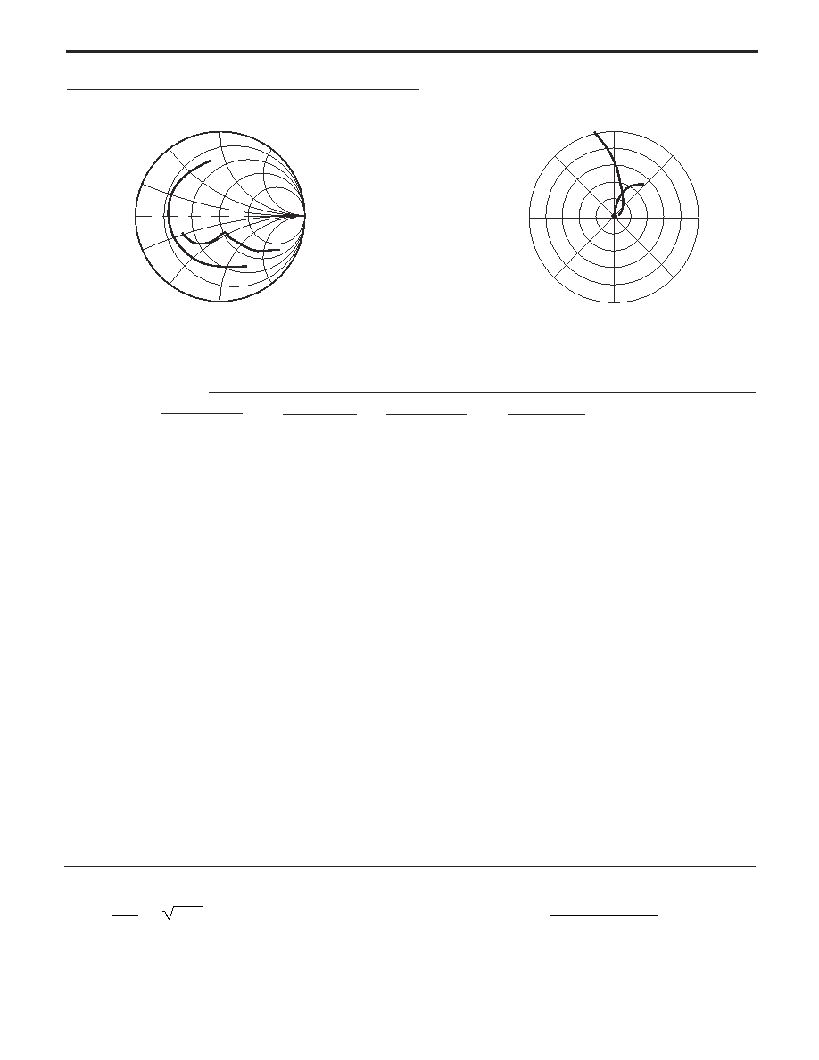
TYPICAL SCATTERING PARAMETERS
(T
A
= 25
°
C)
FREQUENCY
S
11
S
21
S
12
S
22
K
MAG
1
GHz
MAG
ANG
MAG
ANG
MAG
ANG
MAG
ANG
(dB)
NE851M03
V
C
= 2 V, I
C
= 10 mA
0.100
0.695
-61.64
23.158
144.21
0.026
61.44
0.821
-29.68
0.183
29.48
0.200
0.624
-100.58
17.024
122.63
0.038
50.73
0.610
-44.71
0.335
26.51
0.300
0.595
-123.61
12.782
110.30
0.044
47.67
0.480
-51.39
0.469
24.63
0.400
0.582
-137.95
10.071
102.30
0.049
47.72
0.405
-54.57
0.583
23.13
0.500
0.609
-154.61
8.021
95.02
0.052
47.72
0.289
-65.42
0.727
21.91
0.700
0.608
-165.54
5.858
87.23
0.060
52.69
0.245
-68.86
0.876
19.91
1.000
0.608
-175.12
4.192
78.55
0.075
59.31
0.226
-72.02
0.984
17.48
1.100
0.610
-177.63
3.830
76.03
0.080
61.10
0.223
-73.72
1.005
16.36
1.200
0.609
-179.89
3.528
73.70
0.086
62.79
0.221
-75.21
1.026
15.15
1.300
0.608
178.01
3.271
71.35
0.091
64.04
0.223
-77.34
1.039
14.33
1.400
0.608
176.04
3.057
69.13
0.097
65.34
0.226
-78.57
1.044
13.69
1.500
0.608
174.19
2.866
66.99
0.104
66.51
0.229
-80.20
1.045
13.12
1.600
0.609
172.64
2.703
64.95
0.110
67.27
0.232
-81.76
1.043
12.63
1.700
0.609
170.81
2.556
62.92
0.117
68.13
0.237
-83.43
1.040
12.18
1.800
0.608
169.29
2.429
60.94
0.124
68.82
0.241
-85.04
1.033
11.81
1.900
0.607
167.57
2.313
59.01
0.131
69.46
0.247
-86.60
1.027
11.45
2.000
0.606
166.16
2.211
57.16
0.138
70.00
0.252
-88.61
1.023
11.11
2.100
0.607
164.68
2.115
55.16
0.146
70.12
0.258
-90.25
1.011
10.96
2.200
0.606
163.12
2.031
53.46
0.154
70.56
0.266
-91.95
0.999
11.21
2.300
0.605
161.63
1.954
51.71
0.162
70.80
0.271
-93.42
0.990
10.82
2.400
0.606
160.05
1.884
50.01
0.170
70.94
0.278
-94.93
0.979
10.45
2.500
0.606
158.52
1.821
48.31
0.178
70.87
0.285
-96.56
0.966
10.10
2.600
0.605
156.89
1.760
46.64
0.186
70.86
0.291
-98.07
0.957
9.75
2.700
0.606
155.28
1.706
44.97
0.196
70.87
0.299
-99.75
0.941
9.41
2.800
0.604
153.71
1.654
43.40
0.205
70.66
0.306
-101.10
0.931
9.08
2.900
0.603
151.89
1.605
41.82
0.214
70.49
0.314
-102.50
0.922
8.76
3.000
0.604
150.23
1.561
40.28
0.223
69.98
0.321
-104.02
0.907
8.45
3.500
0.602
141.17
1.375
33.08
0.272
68.05
0.357
-111.13
0.862
7.04
4.000
0.604
131.89
1.233
26.63
0.323
64.75
0.391
-118.23
0.823
5.81
4.500
0.607
122.66
1.119
20.91
0.376
60.65
0.421
-126.11
0.805
4.73
5.000
0.614
114.03
1.026
15.94
0.428
55.85
0.448
-134.94
0.799
3.80
5.500
0.625
106.41
0.949
11.68
0.477
50.70
0.471
-144.72
0.805
2.99
6.000
0.638
99.10
0.887
8.19
0.523
45.37
0.489
-154.78
0.821
2.30
Note:
1. Gain Calculations:
MAG =
|S
21
|
|S
12
|
K - 1
).
2
(
K
±
= S
11
S
22
- S
21
S
12
When K
1, MAG is undefined and MSG values are used. MSG =
|S
21
|
|S
12
|
, K = 1 + |
| - |S
11
| - |S
22
|
2
2
2
2 |S
12
S
21
|
,
MAG = Maximum Available Gain
MSG = Maximum Stable Gain
j50
j25
j10
0
10
25
-j10
-j25
-j50
-j100
j100
0
50
100
0
S22
S11
0.100 to 6.000 GHz by 0.100
+90°
+45°
+135°
+180°
1
8
6
4
2
-135°
-90°
-45°
0°
S12
S21
0.100 to 6.000 GHz by 0.100
NE851M03
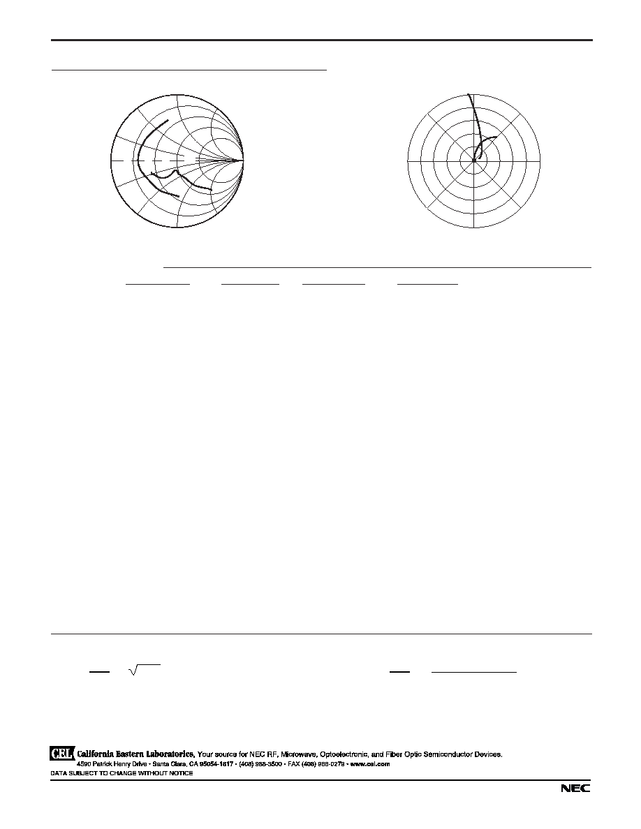
TYPICAL SCATTERING PARAMETERS
(T
A
= 25
°
C)
A Business Partner of NEC Compound Semiconductor Devices, Ltd.
01/29/2003
Note:
1. Gain Calculations:
MAG =
|S
21
|
|S
12
|
K - 1
).
2
(
K
±
= S
11
S
22
- S
21
S
12
When K
1, MAG is undefined and MSG values are used. MSG =
|S
21
|
|S
12
|
, K = 1 + |
| - |S
11
| - |S
22
|
2
2
2
2 |S
12
S
21
|
,
MAG = Maximum Available Gain
MSG = Maximum Stable Gain
FREQUENCY
S
11
S
21
S
12
S
22
K
MAG
1
GHz
MAG
ANG
MAG
ANG
MAG
ANG
MAG
ANG
(dB)
NE851M03
V
C
= 3 V, I
C
= 20 mA
0.100
0.555
-83.93
33.100
134.57
0.020
59.16
0.705
-40.19
0.304
32.17
0.200
0.525
-123.08
21.477
114.01
0.028
53.63
0.469
-55.38
0.529
28.79
0.300
0.519
-141.74
15.332
103.82
0.035
55.51
0.355
-61.29
0.680
26.43
0.400
0.518
-152.59
11.824
97.41
0.040
58.95
0.295
-63.99
0.790
24.68
0.500
0.570
-165.20
9.286
91.94
0.045
60.56
0.203
-82.72
0.896
23.15
0.700
0.572
-173.28
6.730
85.52
0.058
64.80
0.170
-87.94
0.977
20.68
1.000
0.573
179.45
4.793
78.07
0.078
68.73
0.156
-90.92
1.020
17.03
1.100
0.574
177.46
4.376
75.85
0.085
69.69
0.154
-92.65
1.024
16.18
1.200
0.573
175.59
4.030
73.81
0.092
70.12
0.153
-93.73
1.032
15.34
1.300
0.573
173.85
3.736
71.72
0.099
70.66
0.156
-95.63
1.033
14.66
1.400
0.572
172.20
3.490
69.72
0.106
71.00
0.159
-96.09
1.031
14.09
1.500
0.572
170.60
3.272
67.80
0.113
71.20
0.162
-97.01
1.030
13.54
1.600
0.571
169.35
3.086
65.92
0.121
71.30
0.164
-97.84
1.027
13.07
1.700
0.571
167.72
2.918
64.09
0.129
71.48
0.169
-98.85
1.022
12.65
1.800
0.570
166.42
2.772
62.29
0.136
71.38
0.173
-99.61
1.018
12.28
1.900
0.568
164.85
2.641
60.52
0.144
71.29
0.177
-100.52
1.015
11.89
2.000
0.567
163.64
2.524
58.79
0.152
71.21
0.182
-101.75
1.010
11.61
2.100
0.566
162.32
2.415
56.94
0.160
71.07
0.188
-102.94
1.004
11.40
2.200
0.566
160.87
2.321
55.35
0.167
70.95
0.194
-103.84
0.997
11.42
2.300
0.564
159.57
2.233
53.71
0.176
70.63
0.200
-104.57
0.990
11.04
2.400
0.564
158.12
2.155
52.12
0.184
70.33
0.205
-105.29
0.982
10.69
2.500
0.563
156.71
2.082
50.51
0.192
69.89
0.212
-106.25
0.974
10.35
2.600
0.562
155.22
2.013
48.91
0.200
69.69
0.218
-107.15
0.968
10.02
2.700
0.562
153.77
1.953
47.33
0.209
69.30
0.225
-108.26
0.958
9.70
2.800
0.559
152.31
1.895
45.82
0.218
68.85
0.231
-108.94
0.952
9.39
2.900
0.558
150.61
1.840
44.30
0.227
68.41
0.238
-109.85
0.946
9.10
3.000
0.558
149.11
1.791
42.79
0.235
67.76
0.245
-110.73
0.937
8.82
3.500
0.554
140.64
1.583
35.66
0.280
65.12
0.280
-115.50
0.903
7.52
4.000
0.555
132.00
1.426
29.06
0.327
61.75
0.313
-120.66
0.870
6.39
4.500
0.558
123.35
1.300
22.97
0.374
57.82
0.345
-127.21
0.850
5.41
5.000
0.567
115.32
1.196
17.43
0.421
53.51
0.374
-134.94
0.834
4.54
5.500
0.581
108.18
1.109
12.40
0.465
48.92
0.400
-143.93
0.826
3.77
6.000
0.599
101.26
1.034
7.97
0.507
44.18
0.423
-153.49
0.828
3.09
Life Support Applications
These NEC products are not intended for use in life support devices, appliances, or systems where the malfunction of these products can reasonably be expected to
result in personal injury. The customers of CEL using or selling these products for use in such applications do so at their own risk and agree to fully indemnify CEL for
all damages resulting from such improper use or sale.
j50
j25
j10
0
10
25
-j10
-j25
-j50
-j100
j100
0
50
100
0
S22
S11
0.100 to 6.000 GHz by 0.100
+90°
+45°
+135°
+180°
1
8
6
4
2
-135°
-90°
-45°
0°
S12
S21
0.100 to 6.000 GHz by 0.100