 | –≠–ª–µ–∫—Ç—Ä–æ–Ω–Ω—ã–π –∫–æ–º–ø–æ–Ω–µ–Ω—Ç: NE894M13 | –°–∫–∞—á–∞—Ç—å:  PDF PDF  ZIP ZIP |

NE894M13
NPN SILICON TRANSISTOR
∑
NEW MINIATURE M13 PACKAGE:
≠ Small transistor outline
≠ 1.0 X 0.5 X 0.5 mm
≠ Low profile / 0.50 mm package height
≠ Flat lead style for better RF performance
∑
IDEAL FOR > 3 GHz OSCILLATORS
∑
LOW NOISE, HIGH GAIN
∑
LOW C
re
∑
UHSO 25 GHz PROCESS
FEATURES
OUTLINE DIMENSIONS
(Units in mm)
PACKAGE OUTLINE M13
PART NUMBER
NE894M13
EIAJ
1
REGISTERED NUMBER
2SC5787
PACKAGE OUTLINE
M13
SYMBOLS
PARAMETERS AND CONDITIONS
UNITS
MIN
TYP
MAX
f
T
Gain Bandwidth at V
CE
= 1 V, I
C
= 20 mA, f = 2 GHz
GHz
17
20
≠
|S
21E
|
2
Insertion Power Gain at V
CE
= 1 V, I
C
= 20 mA, f = 2 GHz
dB
11
13
≠
|
NF
Noise Figure at V
CE
= 1 V, I
C
= 5 mA, f = 2 GHz, Z
S
= Z
OPT
dB
≠
1.4
2.5
C
re
Reverse Transfer Capacitance
3
at V
CB
= 0.5 V, I
E
= 0 mA, f = 1 MHz
pF
≠
0.22
0.30
I
CBO
Collector Cutoff Current at V
CB
= 5 V, I
E
= 0
nA
≠
≠
100
I
EBO
Emitter Cutoff Current at V
EB
= 1 V, I
C
= 0
nA
≠
≠
100
h
FE
DC Current Gain
2
at V
CE
= 1 V, I
C
= 5 mA
50
≠
100
ELECTRICAL CHARACTERISTICS
(T
A
= 25∞C)
Notes:
1. Electronic Industrial Association of Japan.
2. Pulsed measurement, pulse width 350 µs, duty cycle 2 %.
3. Collector to base capacitance when the emitter is grounded
DESCRIPTION
NEC's NE894M13 transistor is designed for oscillator applica-
tions above 3 GHz. The NE894M13 features low voltage, low
current operation, low noise, and high gain. NEC's new low
profile/flat lead style "M13" package is ideal for today's portable
wireless applications.
California Eastern Laboratories
1. Emitter
2. Base
3. Collector
PIN CONNECTIONS
0.125
+0.1 Ò0.05
0.5±0.05
0.1
0.1
0.2
+0.1 Ò0.05
0.35
0.7
0.35
0.15
+0.1 Ò0.05
0.15
+0.1 Ò0.05
1.0
+0.1 Ò0.05
0.5
+0.1
Ò0.05
0.7±0.05
1
2
3
Y2
0.3
0.2
0.2
(Bottom View)

Notes:
1. Operation in excess of any one of these parameters may result
in permanent damage.
2. With device mounted on 1.08 cm
2
X 1.0 mm glass epoxy board.
SYMBOLS
PARAMETERS
UNITS
RATINGS
V
CBO
Collector to Base Voltage
V
9
V
CEO
Collector to Emitter Voltage
V
3.0
V
EBO
Emitter to Base Voltage
V
1.5
I
C
Collector Current
mA
35
P
T2
Total Power Dissipation
mW
105
T
J
Junction Temperature
∞C
150
T
STG
Storage Temperature
∞C
-65 to +150
ABSOLUTE MAXIMUM RATINGS
1
(T
A
= 25∞C)
Ambient Temperature, T
A
(∞C)
Total Power Dissipation, P
tot
(mW)
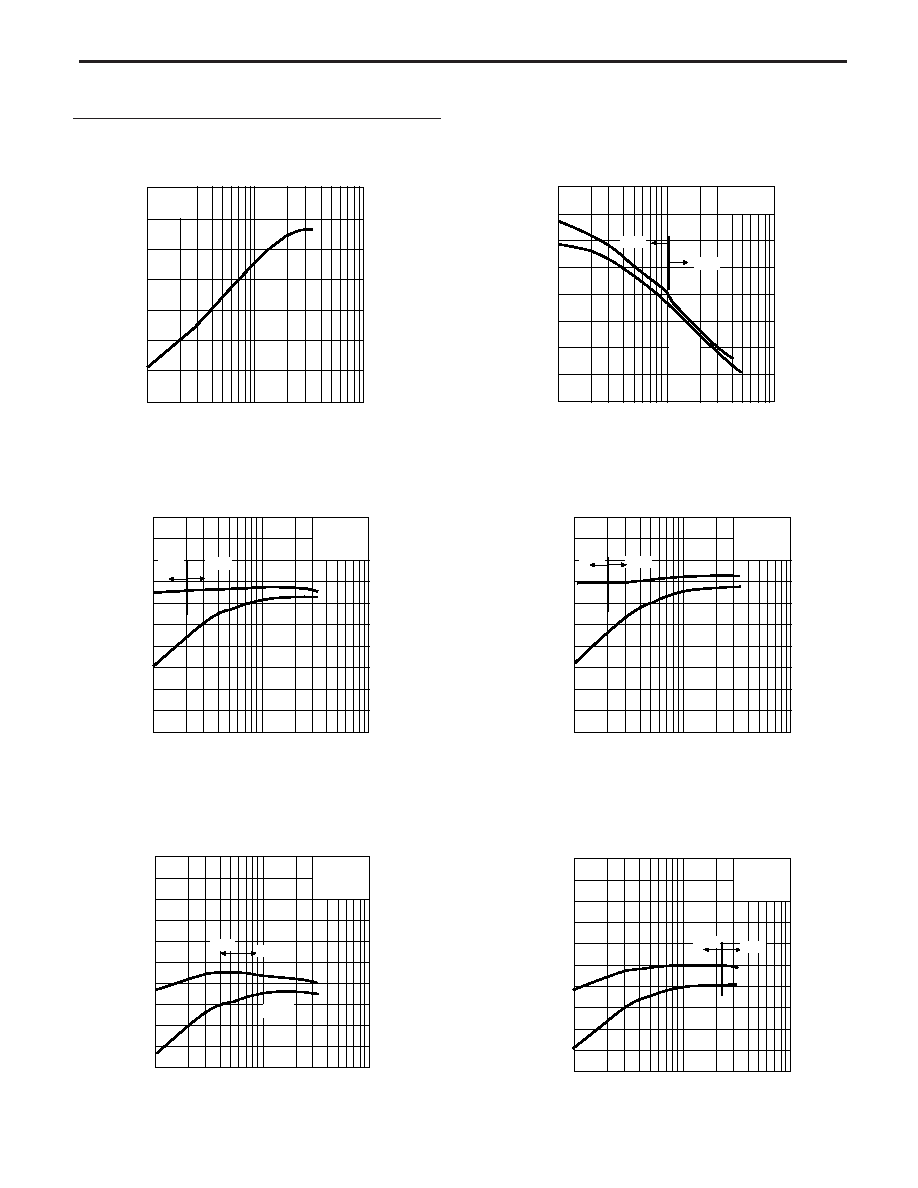
TOTAL POWER DISSIPATION vs.
AMBIENT TEMPERATURE
TYPICAL PERFORMANCE CURVES
(T
A
= 25∞C)
Collector to Base Voltage, V
CB
(V)
Reverse Transfer Capacitance, C
re
(pF)
REVERSE TRANSFR CAPACITANCE vs.
COLLECTOR TO BASE VOLTAGE
150
125
100
75
50
25
0
105
Mounted on Glass epoxy PCB
(1.08 cm
2
x 1.0 mm (t) )
0
25
50
75
100
125
150
0.5
0.4
0.3
0.2
0.1
0
0
2
4
6
8
10
f = 1 MHz
NE894M13
V
CE
= 1 V
100
10
1
0.1
0.001
0.0001
0.01
0.4
0.5
0.6
0.7
0.8
0.9
1.0
Base to Emitter Voltage, V
BE
(V)
Collector Current, I
C
(mA)
COLLECTOR CURRENT vs.
BASE TO EMITTER VOLTAGE
40
30
20
10
0
0
1
2
3
4
5
500 µA
150 µA
200 µA
250 µA
300 µA
350 µA
400 µA
450 µA
100 µA
I
B
= 500 µA
Collector Current, I
C
(mA)
COLLECTOR CURRENT vs.
COLLECTOR TO EMITTER VOLTAGE
Collector to Emitter Voltage, V
CE
(V)
PART NUMBER
QUANTITY
NE894M13-A
NE894M13-T3-A
ORDERING INFORMATION
TYPICAL PERFORMANCE CURVES
(T
A
= 25∞C)
28
24
20
16
12
8
4
0
1
10
100
V
CE
= 1 V
f = 2 GHz
40
35
30
25
20
15
10
5
0
0.1
1
10
MSG
MAG
|S
21e
|
2
V
CE
= 1 V
I
C
= 20 mA
20
16
12
8
4
0
1
10
MSG
MAG
|S
21e
|
2
100
V
CE
= 2 V
f = 2 GHz
20
16
12
8
4
0
1
10
MSG
MAG
|S
21e
|
2
100
V
CE
= 2 V
f = 2 GHz
Collector Current, I
C
(mA)
NE894M13
20
16
12
8
4
0
1
10
100
V
CE
= 1 V
f = 4 GHz
MSG
MAG
|S
21e
|
2
20
16
12
8
4
0
1
10
100
V
CE
= 2 V
f = 4 GHz
MSG
MAG
|S
21e
|
2
Insertion Power Gain, |S
21e
|
2
(dB)
Maximum Available Gain, MAG(dB)
Maximum Stable Gain, MSG(dB)
INSERTION POWER GAIN, MAG, MSG
vs. FREQUENCY
Collector Current, I
C
(mA)
INSERTION POWER GAIN, MAG, MSG
vs. COLLECTOR CURRENT
Associated Gain, G
a
(dB)
Collector Current, I
C
(mA)
Collector Current, I
C
(mA)
Gain Bandwidth Product, f
T
(GHz)
Collector Current, I
C
(mA)
GAIN BANDWIDTH PRODUCT
vs. COLLECTOR CURRENT
Frequency, f (GHz)
Insertion Power Gain, |S
21e
|
2
(dB)
Maximum Available Gain, MAG(dB)
Maximum Stable Gain, MSG(dB)
INSERTION POWER GAIN, MAG, MSG
vs. COLLECTOR CURRENT
Insertion Power Gain, |S
21e
|
2
(dB)
Maximum Available Gain, MAG(dB)
Maximum Stable Gain, MSG(dB)
INSERTION POWER GAIN, MAG, MSG
vs. COLLECTOR CURRENT
Insertion Power Gain, |S
21e
|
2
(dB)
Maximum Available Gain, MAG(dB)
Maximum Stable Gain, MSG(dB)
INSERTION POWER GAIN, MAG, MSG
vs. COLLECTOR CURRENT
Insertion Power Gain, |S
21e
|
2
(dB)
Maximum Available Gain, MAG(dB)
Maximum Stable Gain, MSG(dB)

NE894M13
5
4
3
2
1
0
1
10
100
0
4
8
12
16
20
V
CE
= 1 V
f = 1 GHz
Ga
NF
Noise Figure, NF (dB)
NOISE FIGURE, ASSOCIATED GAIN
vs. COLLECTOR CURRENT
TYPICAL PERFORMANCE CURVES
(T
A
= 25∞C)
Associated Gain, G
a
(dB)
Collector Current, I
C
(mA)
5
4
3
2
1
0
1
10
100
0
4
8
12
16
20
V
CE
= 1 V
f = 2 GHz
Ga
NF
Collector Current, I
C
(mA)
Associated Gain, G
a
(dB)
Noise Figure, NF (dB)
NOISE FIGURE, ASSOCIATED GAIN
vs. COLLECTOR CURRENT

NE894M13
TYPICAL SCATTERING PARAMETERS
(T
A
= 25∞C)
Note:
1. Gain Calculations:
MAG =
|S
21
|
|S
12
|
K - 1
).
2
(
K ±
= S
11
S
22
- S
21
S
12
When K 1, MAG is undefined and MSG values are used. MSG =
|S
21
|
|S
12
|
, K = 1 + | | - |S
11
| - |S
22
|
2
2
2
2 |S
12
S
21
|
,
MAG = Maximum Available Gain
MSG = Maximum Stable Gain
FREQUENCY
S
11
S
21
S
12
S
22
K
MAG
1
GHz
MAG
ANG
MAG
ANG
MAG
ANG
MAG
ANG
(dB)
NE894M13
V
C
= 1 V, I
C
= 5 mA
0.10
0.772
- 11.0
13.002
169.8
0.011
85.6
0.966
- 8.4
0.10
30.55
0.20
0.747
- 24.6
12.548
159.5
0.022
76.8
0.928
- 15.8
0.17
27.54
0.30
0.715
- 36.5
11.948
150.4
0.032
70.6
0.883
- 22.5
0.22
25.75
0.40
0.677
- 47.7
11.241
142.4
0.040
66.2
0.835
- 28.3
0.27
24.50
0.50
0.612
- 59.5
10.457
134.1
0.046
61.3
0.758
- 31.4
0.39
23.57
0.60
0.575
- 68.8
9.699
127.9
0.051
58.2
0.707
- 35.7
0.44
22.79
0.70
0.544
- 76.9
8.993
122.5
0.056
56.5
0.658
- 39.1
0.50
22.09
0.80
0.517
- 84.6
8.364
117.7
0.059
54.9
0.623
- 41.6
0.54
21.50
0.90
0.493
- 91.3
7.756
113.5
0.062
54.1
0.590
- 44.1
0.59
20.94
1.00
0.474
- 97.3
7.228
109.6
0.065
53.6
0.558
- 45.9
0.65
20.46
2.00
0.383
-135.0
4.155
84.4
0.088
58.8
0.411
- 59.5
1.01
16.27
3.00
0.362
-155.9
2.920
68.1
0.120
67.4
0.383
- 73.2
1.10
11.97
4.00
0.355
-175.7
2.253
54.6
0.162
72.0
0.412
- 88.5
1.05
10.08
5.00
0.352
169.2
1.821
44.0
0.215
73.4
0.476
- 98.4
0.95
9.28
6.00
0.339
158.2
1.561
36.0
0.281
72.6
0.512
-103.6
0.86
7.44
7.00
0.359
145.9
1.390
28.0
0.358
68.5
0.522
-114.0
0.81
5.89
8.00
0.394
132.7
1.251
20.9
0.438
62.5
0.523
-127.0
0.79
4.56
9.00
0.432
121.6
1.137
14.9
0.513
55.6
0.521
-142.1
0.80
3.45
10.00
0.466
110.0
1.026
10.5
0.569
48.7
0.543
-157.6
0.84
2.56
11.00
0.489
99.5
0.930
8.9
0.609
43.9
0.572
-165.7
0.87
1.84
12.00
0.489
92.9
0.878
9.3
0.653
40.4
0.567
-168.8
0.90
1.28
0.100 to 12.000 GHz by 0.050
j50
j25
j10
10
25
-j10
-j25
-j50
-j100
j100
0
50
100
0
S
11
S
22
0.100 to 12.000GHz by 0.050
120∞
90∞
60∞
30∞
150∞
180∞
-150∞
-120∞
-90∞
-60∞
-30∞
0∞
S
12
S
21

Note:
1. Gain Calculations:
MAG =
|S
21
|
|S
12
|
K - 1
).
2
(
K ±
= S
11
S
22
- S
21
S
12
When K 1, MAG is undefined and MSG values are used. MSG =
|S
21
|
|S
12
|
, K = 1 + | | - |S
11
| - |S
22
|
2
2
2
2 |S
12
S
21
|
,
MAG = Maximum Available Gain
MSG = Maximum Stable Gain
FREQUENCY
S
11
S
21
S
12
S
22
K
MAG
1
GHz
MAG
ANG
MAG
ANG
MAG
ANG
MAG
ANG
(dB)
NE894M13
V
C
= 1 V, I
C
= 20 mA
0.10
0.401
- 25.4
29.774
160.5
0.009
82.2
0.879
- 15.8
0.40
35.10
0.20
0.374
- 50.1
26.263
145.4
0.018
74.2
0.786
- 28.2
0.45
31.74
0.30
0.345
- 69.6
22.629
133.7
0.024
71.0
0.689
- 37.3
0.54
29.72
0.40
0.323
- 85.0
19.474
124.8
0.029
68.3
0.607
- 43.9
0.63
28.21
0.50
0.290
-100.7
16.742
117.7
0.034
67.8
0.506
- 46.3
0.75
26.95
0.60
0.282
-111.9
14.691
112.3
0.038
67.6
0.450
- 50.3
0.81
25.83
0.70
0.277
-119.6
13.024
108.0
0.043
68.0
0.405
- 53.1
0.86
24.84
0.80
0.274
-126.5
11.685
104.4
0.047
68.5
0.374
- 54.5
0.90
23.94
0.90
0.273
-132.5
10.574
101.2
0.051
69.0
0.349
- 56.2
0.93
23.14
1.00
0.271
-137.0
9.642
98.5
0.056
69.5
0.324
- 57.3
0.95
22.37
2.00
0.272
-162.0
5.122
80.3
0.100
72.3
0.228
- 66.9
1.06
15.65
3.00
0.275
-176.0
3.539
67.7
0.147
71.6
0.221
- 80.0
1.05
12.37
4.00
0.278
167.1
2.723
56.9
0.196
69.5
0.261
- 95.5
1.03
10.35
5.00
0.268
153.9
2.223
47.9
0.245
66.9
0.331
-101.9
0.99
9.58
6.00
0.243
146.2
1.922
40.4
0.300
64.6
0.369
-102.7
0.95
8.07
7.00
0.262
138.9
1.720
32.9
0.360
60.8
0.379
-111.1
0.91
6.80
8.00
0.300
129.8
1.565
25.9
0.421
56.4
0.384
-122.9
0.89
5.70
9.00
0.343
122.0
1.439
19.5
0.482
51.5
0.389
-136.9
0.88
4.75
10.00
0.386
112.1
1.316
13.9
0.532
46.5
0.425
-152.2
0.88
3.93
11.00
0.417
102.2
1.199
10.5
0.572
42.8
0.472
-159.8
0.88
3.21
12.00
0.423
96.7
1.123
8.8
0.617
40.2
0.488
-161.6
0.88
2.60
TYPICAL SCATTERING PARAMETERS
(T
A
= 25∞C)
0.100 to 12.000 GHz by 0.050
j50
j25
j10
10
25
-j10
-j25
-j50
-j100
j100
0
50
100
0
S
11
S
22
120∞
90∞
60∞
30∞
150∞
180∞
-150∞
-120∞
-90∞
-60∞
-30∞
0∞
S
12
S
21
0.100 to 4.000GHz by 0.050
NE894M13
NE894M13
TYPICAL SCATTERING PARAMETERS
(T
A
= 25∞C)
Note:
1. Gain Calculations:
MAG =
|S
21
|
|S
12
|
K - 1
).
2
(
K ±
= S
11
S
22
- S
21
S
12
When K 1, MAG is undefined and MSG values are used. MSG =
|S
21
|
|S
12
|
, K = 1 + | | - |S
11
| - |S
22
|
2
2
2
2 |S
12
S
21
|
,
MAG = Maximum Available Gain
MSG = Maximum Stable Gain
FREQUENCY
S
11
S
21
S
12
S
22
K
MAG
1
GHz
MAG
ANG
MAG
ANG
MAG
ANG
MAG
ANG
(dB)
NE894M13
V
C
= 2 V, I
C
= 10 mA
0.10
0.634
- 14.2
21.168
166.5
0.010
85.7
0.945
- 10.0
0.19
33.43
0.20
0.601
- 30.0
19.847
154.5
0.017
75.7
0.890
- 18.5
0.28
30.64
0.30
0.559
- 43.3
18.259
144.2
0.024
70.8
0.826
- 25.6
0.36
28.79
0.40
0.515
- 55.3
16.598
135.6
0.029
67.6
0.763
- 31.2
0.43
27.51
0.50
0.451
- 67.4
14.913
127.5
0.034
64.9
0.676
- 33.5
0.56
26.40
0.60
0.417
- 77.1
13.497
121.5
0.038
63.7
0.621
- 37.1
0.62
25.49
0.70
0.391
- 84.8
12.240
116.5
0.042
63.5
0.572
- 39.6
0.68
24.65
0.80
0.369
- 92.2
11.177
112.3
0.045
63.2
0.539
- 41.3
0.73
23.93
0.90
0.351
- 98.6
10.239
108.5
0.049
63.5
0.510
- 42.9
0.78
23.24
1.00
0.337
-104.1
9.431
105.2
0.052
63.9
0.481
- 43.9
0.82
22.61
2.00
0.279
-137.6
5.194
83.8
0.084
70.4
0.363
- 52.7
1.04
16.74
3.00
0.266
-155.9
3.616
69.6
0.123
74.0
0.345
- 64.5
1.05
13.31
4.00
0.262
-175.2
2.787
57.5
0.168
74.7
0.373
- 79.7
1.00
11.92
5.00
0.255
170.3
2.259
47.6
0.217
73.9
0.439
- 89.6
0.93
10.17
6.00
0.237
161.9
1.936
39.8
0.276
72.7
0.483
- 93.7
0.86
8.47
7.00
0.259
151.8
1.731
32.0
0.344
69.3
0.499
-102.7
0.81
7.02
8.00
0.300
139.9
1.571
24.6
0.418
64.4
0.505
-114.4
0.78
5.75
9.00
0.347
129.8
1.439
17.8
0.493
58.5
0.508
-128.5
0.77
4.65
10.00
0.392
117.8
1.303
12.0
0.555
52.3
0.535
-144.5
0.78
3.71
11.00
0.425
106.1
1.170
8.7
0.600
47.5
0.573
-153.9
0.80
2.90
12.00
0.433
99.2
1.080
7.5
0.648
44.1
0.581
-157.6
0.82
2.22
0.100 to 12.000 GHz by 0.050
j50
j25
j10
10
25
-j10
-j25
-j50
-j100
j100
0
50
100
0
S
11
S
22
0.100 to 12.000GHz by 0.050
120∞
90∞
60∞
30∞
150∞
180∞
-150∞
-120∞
-90∞
-60∞
-30∞
0∞
S
12
S
21

EXCLUSIVE NORTH AMERICAN AGENT FOR NEC RF, MICROWAVE & OPTOELECTRONIC SEMICONDUCTORS
CALIFORNIA EASTERN LABORATORIES ∑ Headquarters ∑ 4590 Patrick Henry Drive ∑ Santa Clara, CA 95054-1817 ∑ (408) 988-3500 ∑ Telex 34-6393 ∑ FAX (408) 988-0279
Internet: http://WWW.CEL.COM
03/18/2002
DATA SUBJECT TO CHANGE WITHOUT NOTICE
Life Support Applications
These NEC products are not intended for use in life support devices, appliances, or systems where the malfunction of these products can reasonably
be expected to result in personal injury. The customers of CEL using or selling these products for use in such applications do so at their own risk and
agree to fully indemnify CEL for all damages resulting from such improper use or sale.
NE894M13
Parameters
Q1
Parameters
Q1
IS
137e-18
MJC
0.24
BF
129
XCJC
0.3
NF
0.9992
CJS
0
VAF
22.4
VJS
0.75
IKF
2.8
MJS
0
ISE
229e-15
FC
0.55
NE
2.5
TF
5e-12
BR
81.7
XTF
0.05
NR
0.9944
VTF
0.5
VAR
1.9
ITF
0.005
IKR
0.018
PTF
0
ISC
227e-18
TR
1.0e-9
NC
1.17
EG
1.11
RE
0.75
XTB
0
RB
5
XTI
3
RBM
3
KF
117e-15
IRB
0.005
AF
1.34
RC
6
CJE
0.68e-12
VJE
0.92
MJE
0.26
CJC
0.16e-12
VJC
0.64
(1) Gummel-Poon Model
SCHEMATIC
Parameters
NE894M13
C
CB
0.01 pF
C
CE
0.4 pF
L
B
0.3 nH
L
E
0.42 nH
C
CBPKG
0.05 pF
C
CEPKG
0.05 pF
L
BX
0.05 nH
L
CX
0.05 nH
L
EX
0.05 nH
ADDITIONAL PARAMETERS
MODEL TEST CONDITIONS
Frequency:
0.1 to 10 GHz
Bias:
V
CE
= 0.5 V to 2 V, I
C
= 0.5 mA to 20 mA
Date:
11/2001
BJT NONLINEAR MODEL PARAMETERS
(1)
Base
Emitter
Collector
L
BPKG
0.05 nH
L
B
0.3 nH
L
EPKG
0.05 nH
L
E
0.42 nH
L
CPKG
0.05 nH
C
CBPKG
0.05 pF
C
CB
0.01 pF
C
CE
0.4 pF
C
CEPKG
0.05 pF
Q
1
NONLINEAR MODEL
4590 Patrick Henry Drive
Santa Clara, CA 95054-1817
Telephone: (408) 919-2500
Facsimile: (408) 988-0279
Subject: Compliance with EU Directives
CEL certifies, to its knowledge, that semiconductor and laser products detailed below are compliant
with the requirements of European Union (EU) Directive 2002/95/EC Restriction on Use of Hazardous
Substances in electrical and electronic equipment (RoHS) and the requirements of EU Directive
2003/11/EC Restriction on Penta and Octa BDE.
CEL Pb-free products have the same base part number with a suffix added. The suffix ≠A indicates
that the device is Pb-free. The ≠AZ suffix is used to designate devices containing Pb which are
exempted from the requirement of RoHS directive (*). In all cases the devices have Pb-free terminals.
All devices with these suffixes meet the requirements of the RoHS directive.
This status is based on CEL's understanding of the EU Directives and knowledge of the materials that
go into its products as of the date of disclosure of this information.
Restricted Substance
per RoHS
Concentration Limit per RoHS
(values are not yet fixed)
Concentration contained
in CEL devices
-A
-AZ
Lead (Pb)
< 1000 PPM
Not Detected
(*)
Mercury
< 1000 PPM
Not Detected
Cadmium
< 100 PPM
Not Detected
Hexavalent Chromium
< 1000 PPM
Not Detected
PBB
< 1000 PPM
Not Detected
PBDE
< 1000 PPM
Not Detected
If you should have any additional questions regarding our devices and compliance to environmental
standards, please do not hesitate to contact your local representative.
Important Information and Disclaimer: Information provided by CEL on its website or in other communications concerting the substance
content of its products represents knowledge and belief as of the date that it is provided. CEL bases its knowledge and belief on information
provided by third parties and makes no representation or warranty as to the accuracy of such information. Efforts are underway to better
integrate information from third parties. CEL has taken and continues to take reasonable steps to provide representative and accurate
information but may not have conducted destructive testing or chemical analysis on incoming materials and chemicals. CEL and CEL
suppliers consider certain information to be proprietary, and thus CAS numbers and other limited information may not be available for
release.
In no event shall CEL's liability arising out of such information exceed the total purchase price of the CEL part(s) at issue sold by CEL to
customer on an annual basis.
See CEL Terms and Conditions for additional clarification of warranties and liability.