
NESG250134
NEC's NPN SiGe RF TRANSISTOR
FOR MEDIUM OUTPUT POWER
AMPLIFICATION (800 mW)
3-PIN POWER MINIMOLD (34 PACKAGE)
California Eastern Laboratories
∑
THIS PRODUCT IS SUITABLE FOR
MEDIUM OUTPUT POWER (800 mW) AMPLIFICATION
P
O
= 29 dBm TYP. @ V
CE
= 3.6 V, P
in
= 15 dBm, f = 460 MHz
P
O
= 29 dBm TYP. @ V
CE
= 3.6 V, P
in
= 20 dBm, f = 900 MHz
∑ MAXIMUM STABLE GAIN:
MSG
= 23 dB TYP @ V
CE
= 3.6 V, I
C
= 100 mA, f = 460 MHz
∑
SiGe TECHNOLOGY:
UHS2-HV process
∑
ABSOLUTE MAXIMUM RATINGS:
V
CBO
= 20 V
∑
3-PIN POWER MINIMOLD (34 PACKAGE)
FEATURES
ORDERING INFORMATION
Remark To order evaluation samples, contact your nearby sales office.
Unit sample quantity is 25 pcs.
ABSOLUTE MAXIMUM RATINGS
(T
A
=+25∫C)
Note Mounted on 34.2 cm
2
◊ 0.8 mm (t) glass epoxy PWB
PART NUMBER
ORDER NUMBER
PACKAGE
QUANTITY
SUPPLYING FORM
NESG250134-AZ
NESG250134-AZ
3-pin power minimold
(Pb-Free)
Note1
25 pcs (Non reel) ∑ 12 mm wide embossed taping
∑ Pin 2 (Emitter) face the perforation side of the tape
NESG250134-T1-AZ NESG250134-T1-AZ
1 kpcs/reel
PARAMETER
SYMBOL
RATINGS
UNIT
Collector to Base Voltage
V
CBO
20
V
Collector to Emitter Voltage
V
CEO
9.2
V
Emitter to Base Voltage
V
EBO
2.8
V
Collector Current
I
C
500
mA
Total Power Dissipation
P
tot
Note
1.5
W
Junction Temperature
T
j
150
∞
C
Storage Temperature
T
stg
-
65 to +150
∞
C
Caution Observe precautions when handling because these devices are sensitive to electrostatic discharge.
Note 1. Contains lead in the part except the electrode terminals.

NESG250134
NESG250134
THERMAL RESISTANCE
(T
A
= 25∞C)
PARAMETER
SYMBOL
RATINGS
UNIT
Thermal Resistance from Junction to Ambient
Note
Rth
j-a
80
∞
C/W
Note Mounted on 34.2 cm
2
◊ 0.8 mm (t) glass epoxy PWB
RECOMMENDED OPERATING RANGE
(T
A
= 25∞C)
PARAMETER
SYMBOL
MIN.
TYP.
MAX.
UNIT
Collector to Emitter Voltage
V
CE
-
3.6
4.5
V
Collector Current
I
C
-
400
500
mA
Input Power
Note
P
in
-
12
17
dBm
Note Input power under conditions of V
CE
4.5 V, f = 460 MHz
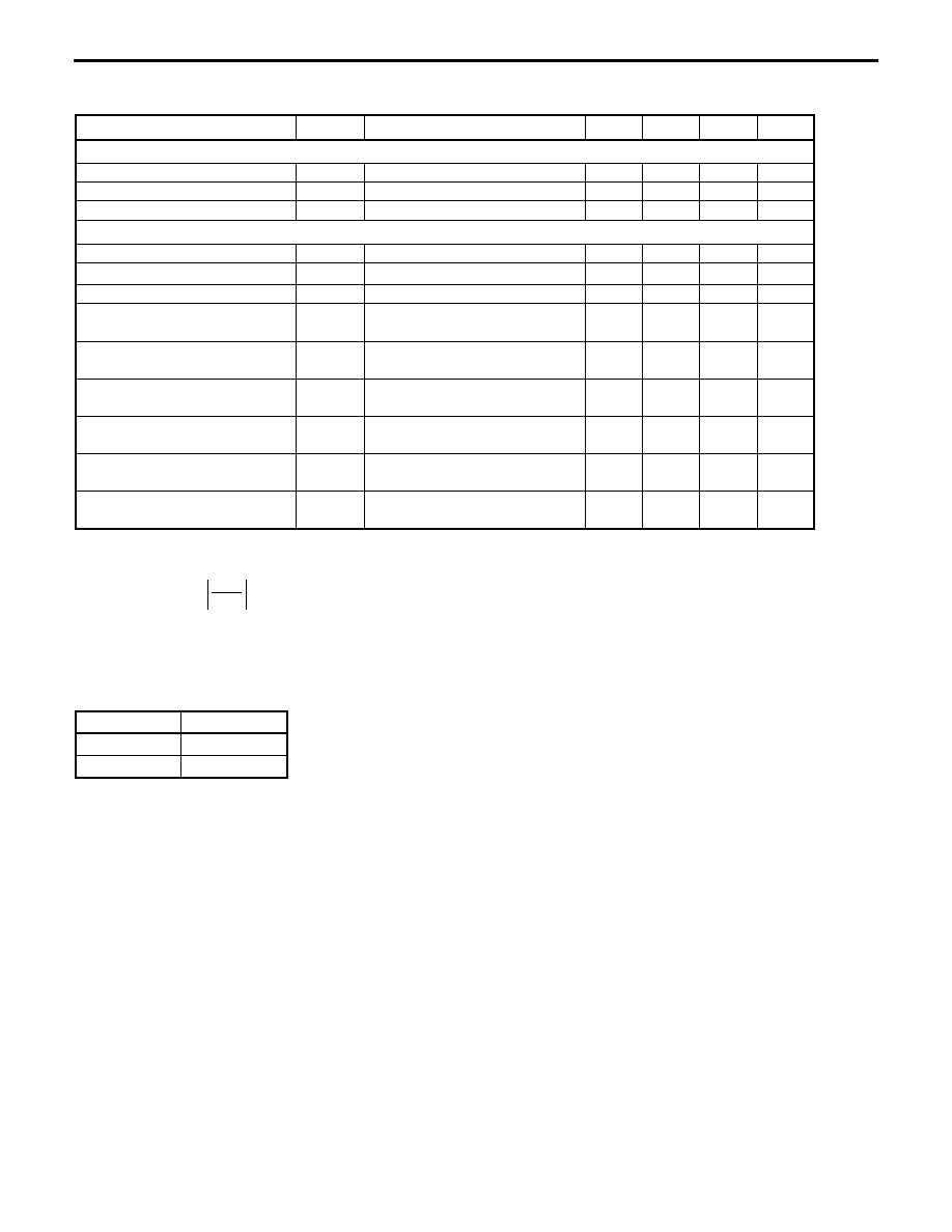
Notes 1. Pulse measurement: PW 350 s, Duty Cycle 2%
2. MSG = S
21
S
12
h
FE
CLASSIFICATION
NESG250134
NESG250134
ELECTRICAL CHARACHTERISTICS
(T
A
= 25∞C)
PARAMETER
SYMBOL
TEST CONDITIONS
MIN.
TYP.
MAX.
UNIT
DC Characteristics
Collector Cut-off Current
I
CBO
V
CB
= 5 V, I
E
= 0 mA
-
-
1
A
Emitter Cut-off Current
I
EBO
V
EB
= 0.5 V, I
C
= 0 mA
-
-
1
A
DC Current Gain
h
FE
Note 1
V
CE
= 3 V, I
C
= 100 mA
80
120
180
-
RF Characteristics
Gain Bandwidth Product
f
T
V
CE
= 3.6 V, I
C
= 100 mA, f = 460 MHz
-
10
-
GHz
Insertion Power Gain
|
S
21e
|
2
V
CE
= 3.6 V, I
C
= 100 mA, f = 460 MHz
-
19
-
dB
Maximum Stable Gain
MSG
Note 2
V
CE
= 3.6 V, I
C
= 100 mA, f = 460 MHz
-
23
-
dB
Linear gain (1)
G
L
V
CE
= 3.6 V, I
C (set)
= 30 mA (RF OFF),
f = 460 MHz, P
in
= 0 dBm
16
19
-
dB
Linear gain (2)
G
L
V
CE
= 3.6 V, I
C (set)
= 30 mA (RF OFF),
f = 900 MHz, P
in
= 0 dBm
-
16
-
dB
Output Power (1)
Po
V
CE
= 3.6 V, I
C (set)
= 30 mA (RF OFF),
f = 460 MHz, P
in
= 15 dBm
27
29
-
dBm
Output Power (2)
Po
V
CE
= 3.6 V, I
C (set)
= 30 mA (RF OFF),
f = 900 MHz, P
in
= 20 dBm
-
29
-
dBm
Collector Efficiency (1)
c
V
CE
= 3.6 V, I
C (set)
= 30 mA (RF OFF),
f = 460 MHz, P
in
= 15 dBm
-
60
-
%
Collector Efficiency (2)
c
V
CE
= 3.6 V, I
C (set)
= 30 mA (RF OFF),
f = 900 MHz, P
in
= 20 dBm
-
60
-
%
RANK
FB
Marking
SN
h
FE
Value
80 to 180

NESG250134
NESG250134
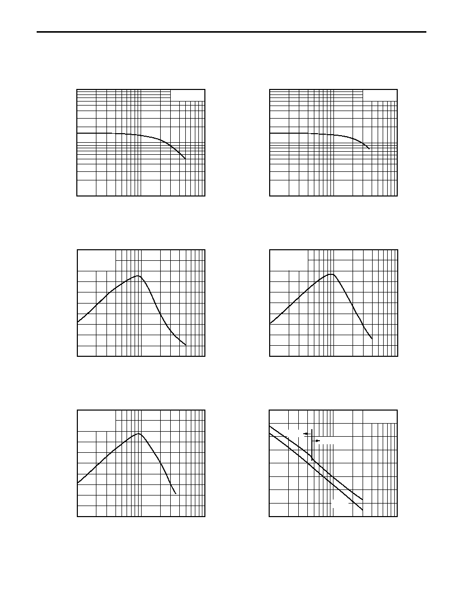
TYPICAL CHARACHTERISTICS
(T
A
= +25∞C, unless otherwise specified )
1.6
1.2
1.0
0.6
0.2
0
2
4
6
8
10
f = 1 MHz
1.4
0.8
0.4
V
CE
= 3 V
100
10
1
0.01
0.001
0.1
0.0001
0.7
0.5
0.6
0.4
0.8
0.9
1.0
1,000
V
CE
= 4 V
100
10
1
0.01
0.001
0.1
0.0001
0.7
0.5
0.6
0.4
0.8
0.9
1.0
1,000
200
500
300
100
0
2
1
3
5
I
B
= 1 mA
4 mA
6 mA
2 mA
10 mA
3 mA
5 mA
8 mA
9 mA
7 mA
400
4
Reverse T
ransfer Capacitance
C
re
(pF)
Collector to Base Voltage V
CB
(V)
REVERSE TRANSFER CAPACITANCE
vs. COLLECTOR TO BASE VOLTAGE
Collector Current
I
C
(mA)
Base to Emitter Voltage V
BE
(V)
COLLECTOR CURRENT vs.
BASE TO EMITTER VOLTAGE
Collector Current
I
C
(mA)
Base to Emitter Voltage V
BE
(V)
COLLECTOR CURRENT vs.
BASE TO EMITTER VOLTAGE
Collector Current
I
C
(mA)
Collector to Emitter Voltage V
CE
(V)
COLLECTOR CURRENT vs.
COLLECTOR TO EMITTER VOLTAGE
T
o
tal Power Dissipation
P
to
t
(mW)
Ambient Temperature T
A
(∫C)
TOTAL POWER DISSIPATION
vs. AMBIENT TEMPERATURE
2.0
1.6
1.5
1.2
0.8
0.4
0
25
50
75
100
125
150
Nature Neglect
Mounted on Glass epoxy PWB
(34.2 cm
2
◊ 0.8 mm (t) )
Remark The graphs indicate nominal characteristics.
NESG250134
NESG250134
1,000
100
10
100
10
1,000
V
CE
= 3 V
1,000
100
10
100
10
1,000
V
CE
= 4 V
20
16
12
8
4
0
10
100
1,000
V
CE
= 3 V
f = 460 MHz
20
16
12
8
4
0
10
100
1,000
V
CE
= 3.6 V
f = 460 MHz
20
16
12
8
4
0
10
100
1,000
V
CE
= 4 V
f = 460 MHz
V
CE
= 3 V
I
C
= 100 mA
40
30
25
20
15
10
5
0
0.1
1
10
MAG
MSG
|S
21e
|
2
35
DC Current Gain
h
FE
Collector Current I
C
(mA)
DC CURRENT GAIN vs.
COLLECTOR CURRENT
DC Current Gain
h
FE
Collector Current I
C
(mA)
DC CURRENT GAIN vs.
COLLECTOR CURRENT
Gain Bandwidth Product
f
T
(GHz)
Collector Current I
C
(mA)
GAIN BANDWIDTH PRODUCT
vs. COLLECTOR CURRENT
Gain Bandwidth Product
f
T
(GHz)
Collector Current I
C
(mA)
GAIN BANDWIDTH PRODUCT
vs. COLLECTOR CURRENT
Gain Bandwidth Product
f
T
(GHz)
Collector Current I
C
(mA)
GAIN BANDWIDTH PRODUCT
vs. COLLECTOR CURRENT
Frequency f (GHz)
INSERTION POWER GAIN,
MAG, MSG vs. FREQUENCY
Insertion Power Gain |S
21e
|
2
(dB)
Maximum Available Power Gain MAG (dB) Maximum Stable Power Gain MSG (dB)
Remark The graphs indicate nominal characteristics.