
4 PIN SOP, 0.9
,
LOW ON-STATE RESISTANCE
80 V BREAK DOWN VOLTAGE,
500 mA CONTINUOUS LOAD CURRENT
1-CH OPTICAL COUPLED MOSFET
PS7205B-1A
FEATURES
∑ LOW ON-STATE RESISTANCE:
Ron = 0.9
TYP
∑ LARGE CONTINUOUS LOAD CURRENT:
I
L
= 500 mA
∑ HIGH-SPEED SWITCHING TIME:
ton, toff = 0.5 ms MAX
∑ 1 CHANNEL TYPE
1 a output
∑ DESIGNED FOR AC/DC SWITCHING LINE CHANGER
∑ SMALL AND THIN PACKAGE:
4-pin SOP, Height = 2.1 mm
∑ HIGH ISOLATION VOLTAGE:
BV = 1 500 Vr.m.s.
∑ LOW OFFSET VOLTAGE
∑ AVAILABLE IN TAPE AND REEL:
PS7205B-1A-E3, E4, F3, F4
DESCRIPTION
The PS7205B-1A is a low on-state resistance solid state relay
containing a GaAs LED on the input side and MOS FETs on
the output side. It is suitable for PLC, etc. because of its large
continuous load current and low on-state resistance.
California Eastern Laboratories
APPLICATIONS
∑ MEASUREMENT EQUIPMENT
∑ FA EQUIPMENT
PART NUMBER
PS7205B-1A
SYMBOLS
PARAMETERS
UNITS
MIN
TYP
MAX
V
F
Forward Voltage
I
F
= 5 mA
V
1.1
1.4
I
R
Reverse Current
V
R
= 5 V
µ
A
5.0
I
Loff
Off-state Leakage Current
V
D
= 80 V
nA
0.15
5.0
C
out
Output Capacitance
V
D
= 0 V, f = 1 MHz
pF
30
I
Fon
LED On-state Current
I
L
= 500 mA
mA
2.0
R
on
On-state Resistance
I
F
= 5 mA, I
L
= 500 mA, t
10 ms
0.9
1.2
t
on
Turn-on Time
1, 2
I
F
= 5 mA, V
O
= 5 V, R
L
= 500
,
ms
0.18
0.5
t
off
Turn-off Time
1, 2
PW
10 ms
0.04
0.5
R
I-O
Isolation Resistance
V
I-O
= 1.0 kV
DC
10
9
C
I-O
Isolation Capacitance
V = 0 V, f = 1 MHz
pF
0.5
Notes:
1.Test Circuit for Switching Time:
2. The turn-on time and turn-off time are specified as input-pulse width
10 ms.
Be aware that when the device operates with an input-pulse width of under 10 ms, the turn-on time and turn-off time will increase.
Output
Input
t
on
t
off
10%
90%
0
V
O
= 5 V
50%
V
L
R
L
I
F
R
in
Pulse Input
Input monitor
monitor
V
O
Diode
Coupled
ELECTRICAL CHARACTERISTICS
(T
A
= 25
∞
C)
MOSFET

ABSOLUTE MAXIMUM RATINGS
1
(T
A
= 25
∞
C)
Notes:
1. Operation in excess of any one of these parameters may result
in permanent damage.
2. PW = 100
µ
s, Duty Cycle = 1%.
3. PW = 100 ms, 1 shot.
4. AC voltage for 1 minute at T
A
= 25
∞
C, RH = 60% between input
and output.
PS7205B-1A
OUTLINE DIMENSIONS
(Units in mm)
4
3
1
2
TOP VIEW
4.4
7.0±0.3
0.5±0.3
0.15
+0.10 -0.05
2.54
4.0±0.5
0.05
+0.08 -0.05
2.05
+0.08 -0.05
0.40
+0.10
-0.05
0.25 M
1. LED Anode
2. LED Cathode
3. MOS FET
4. MOS FET
SYMBOLS
PARAMETERS
UNITS
RATINGS
Diode
I
F
Forward Current (DC)
mA
50
V
R
Reverse Voltage
V
5.0
P
D
Power Dissipation
mW
50
I
FP
Peak Forward Current
2
A
1
MOS FET
V
L
Break Down Voltage
V
80
I
L
Continuous Load Current
mA
500
I
LP
Pulse Load Current
A
1
(AC/DC Connection)
P
D
Power Dissipation
mW
300
Coupled
BV
Isolation Voltage
4
Vr.m.s.
1 500
P
T
Total Power Dissipation
mW
350
T
A
Operating Ambient
∞
C
-
40 to +85
Temperature
T
stg
Storage Temperature
∞
C
-
40 to +100
PART NUMBER
PACKAGE
PACKING STYLE
PS7205B-1A
4-pin SOP
Magazine case
100 pcs
PS7205B-1A-E3
Embossed Tape
900 pcs/reel
PS7205B-1A-E4
PS7205B-1A-F3
Embossed Tape
3 500 pcs/reel
PS7205B-1A-F4
205B
001
001
N
Week Assembled
Year Assembled
(Last 1 Digit)
Nothing
Ink marking
Laser marking
No.1 pin Mark
*1 Applicable type numbers
are underlined below
Rank Code
Assembly Lot
Type Number
*1
PS7205B-1A
MARKING
RECOMMENDED
OPERATING CONDITIONS
(T
A
= 25
∞∞
∞∞
∞
C)
SYMBOLS
PARAMETER
UNITS MIN
TYP MAX
I
F
LED Operating Current
mA
2
5
20
V
F
LED Off Voltage
V
0
0.5
ORDERING INFORMATION
100
85
75
50
25
0
-25
20
60
80
100
40
0
Maximum Forward Current I
F
(mA)
Ambient Temperature T
A
(∞C)
20
10
30
40
35
30
25
20
15
10
5
0
Output Capacitance C
out
(pF)
Applied Voltage V
D
(V)
100
75
0
-25
50
25
600
500
400
300
200
100
0
Maximum Load Current I
L
(mA)
Ambient Temperature T
A
(∞C)
100
0
-25
25
50
75
1.0
1.4
1.6
1.8
1.2
0.8
Forward Voltage V
F
(V)
Ambient Temperature T
A
(∞C)
Load Current I
L
(mA)
Load Voltage V
L
(V)
-0.8
-0.4
0.8
0.4
-250
-750
-500
250
750
500
I
F
= 5 mA,
I
L
= 500 mA
0
85
10
-6
10
-11
10
-8
10
-7
10
-9
10
-10
0
60
20
80
100
120
40
Off-state Leakage Current I
Loff
(A)
Ambient Temperature T
A
(∞C)
f = 1 MHz
V
D
= 80 V
I
F
= 50 mA
30 mA
20 mA
10 mA
5 mA
1 mA
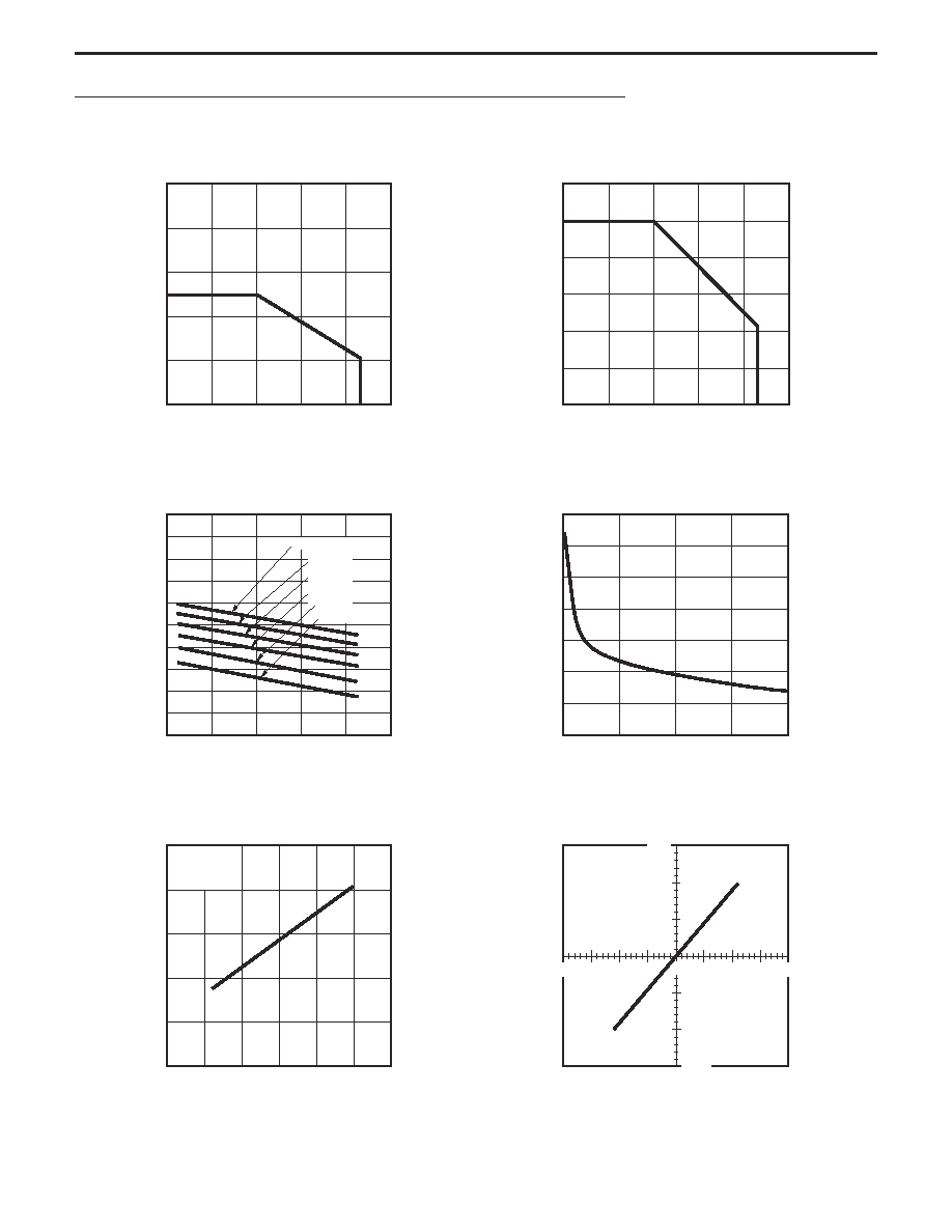
TYPICAL PERFORMANCE CURVES
(T
A
= 25
∞
C, unless otherwise specified)
PS7205B-1A
MAXIMUM FORWARD CURRENT vs
AMBIENT TEMPERATURE
MAXIMUM LOAD CURRENT vs
AMBIENT TEMPERATURE
OUTPUT CAPACITANCE vs.
APPLIED VOLTAGE
FORWARD VOLTAGE vs.
AMBIENT TEMPERATURE
OFF-STATE LEAKAGE CURRENT vs.
AMBIENT TEMPERATURE
LOAD CURRENT vs. LOAD VOLTAGE
0.5
1.5
2.0
3.0
1.0
2.5
0.0
100
75
50
25
-25
0
Normalized On-state Resistance R
on
Ambient Temperature T
A
(∞C)
n = 50 pcs,
I
F
= 5 mA,
I
L
= 500 mA,
t 10 ms
0.85
0.95
1.05
0.90
1.0
0
10
20
30
40
50
60
Number (pcs)
On-state Resistance R
on
(
)
20
10
5
15
1.8
1.6
1.4
1.2
1.0
0.8
0.6
0.4
0.2
0
20
10
5
15
0.10
0.09
0.08
0.07
0.06
0.05
0.04
0.03
0.01
0.02
0
Turn-on Time t
on
(ms)
Forward Current I
F
(mA)
Turn-off Time t
off
(ms)
Forward Current I
F
(mA)
V
O
= 5 V,
R
L
= 500
0.04
0.03
0.05 0.06
0.07
0
10
20
30
40
50
60
Number (pcs)
Turn-off Time t
off
(ms)
n = 50 pcs,
I
F
= 5 mA,
V
O
= 5 V,
R
L
= 500
0.18
0.24
0.16
0.22
0.20
0
10
20
30
40
50
60
Number (pcs)
Turn-on Time t
on
(ms)
n = 50 pcs,
I
F
= 5 mA,
V
O
= 5 V,
R
L
= 500
V
O
= 5 V,
R
L
= 500
Normalized to 1.0
at T
A
= 25∞C,
I
F
= 5 mA,
I
L
= 500 mA
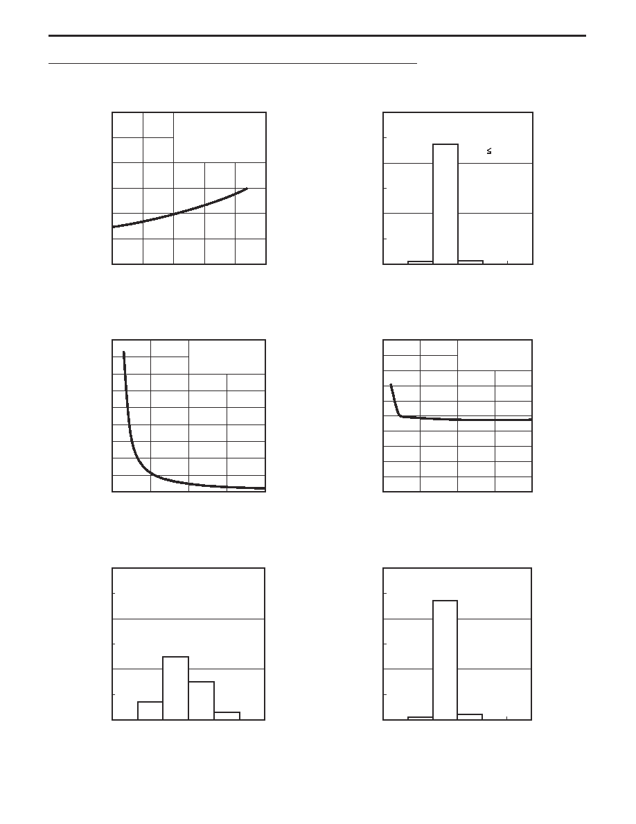
TYPICAL PERFORMANCE CURVES
(T
A
= 25
∞
C, unless otherwise specified)
PS7205B-1A
TURN-ON TIME DISTRIBUTION
TURN-OFF TIME DISTRIBUTION
TURN-ON TIME vs. FORWARD CURRENT
TURN-OFF TIME vs. FORWARD CURRENT
NORMALIZED ON-STATE RESISTANCE
vs. AMBIENT TEMPERATURE
ON-STATE RESISTANCE DISTRIBUTION

TYPICAL PERFORMANCE CURVES
(T
A
= 25
∞
C, unless otherwise specified)
PS7205B-1A
100
0
-25
25
50
75
2.5
3.0
0.0
2.0
1.5
1.0
0.5
Normalized Turn-on Time t
on
Ambient Temperature T
A
(∞C)
100
0
-25
25
50
75
2.5
3.0
0.0
2.0
1.5
1.0
0.5
Normalized Turn-off Time t
off
Ambient Temperature T
A
(∞C)
Normalized to 1.0
at T
A
= 25∞C,
I
F
= 5 mA,
V
O
= 5 V
R
L
= 500
Normalized to 1.0
at T
A
= 25∞C,
I
F
= 5 mA,
V
O
= 5 V
R
L
= 500
NORMALIZED TURN-ON TIME vs.
AMBIENT TEMPERATURE
NORMALIZED TURN-OFF TIME vs.
AMBIENT TEMPERATURE

PS7205B-1A
PS7205B-1A-E3
PS7205B-1A-E4
180
60
13.0±0.5
21.0±0.8
13.0±1.0
2.0±0.5
13.0±0.5
15∞
15∞
2.0
Tape Outline and Dimensions
Tape Direction
Reel Outline and Dimensions
Packing: 900 pcs/reel
1.55±0.1
2.0±0.05
4.0±0.1
1.75±0.1
4.6±0.1
2.9 MAX.
7.4±0.1
0.3
8.0±0.1
1.5
+0.1
-0
5.5±0.05
12.0±0.2
2.4±0.1
TAPING SPECIFICATIONS
(Units in mm)

PS7205B-1A-F3
PS7205B-1A-F4
12.4
+2.0
-0.0
1.5
80±5.0
13.0±0.5
330
1.5±0.5
2.0±0.5
6.0±1
120
∞
60
∞
21.0±0.8
Tape Outline and Dimensions
Tape Direction
Reel Outline and Dimensions
Packing: 3 500 pcs/reel
1.55±0.1
2.0±0.05
4.0±0.1
1.75±0.1
4.6±0.1
2.9 MAX.
7.4±0.1
0.3
8.0±0.1
1.5
+0.1
-0
5.5±0.05
12.0±0.2
2.4±0.1
TAPING SPECIFICATIONS
(Units in mm)
PS7205B-1A

220∞C
Package Surface Temperature T (∞C)
Time (s)
(heating)
to 10 s
to 60 s
260∞C MAX.
Recommended Temperature Profile of Infrared Reflow
120±30 s
(preheating)
180∞C
120∞C
PS7205B-1A
EXCLUSIVE NORTH AMERICAN AGENT FOR NEC RF, MICROWAVE & OPTOELECTRONIC SEMICONDUCTORS
CALIFORNIA EASTERN LABORATORIES ∑ Headquarters ∑ 4590 Patrick Henry Drive ∑ Santa Clara, CA 95054-1817 ∑ (408) 988-3500 ∑ Telex 34-6393 ∑ FAX (408) 988-0279
Internet: http://WWW.CEL.COM
03/04/2002
DATA SUBJECT TO CHANGE WITHOUT NOTICE
RECOMMENDED SOLDERING CONDITIONS
(1) Infrared reflow soldering
∑ Peak reflow temperature
260
∞
C or below (package surface temperature)
∑ Time of peak reflow temperature
10 seconds or less
∑ Time of temperature higher than 220
∞
C
60 seconds or less
∑ Time to preheat temperature from 120 to 180
∞
C
120
±
30 s
∑ Number of reflows
Three
∑ Flux
Rosin flux containing small amount of chlorine
(The flux with a maximum chlorine content of 0.2 Wt % is recommended.)
(2) Wave soldering
∑ Temperature
260
∞
C or below (molten solder temperature)
∑ Time
10 seconds or less
∑ Preheating conditions
120
∞
C or below (package surface temperature)
∑ Number of times
One (Allowed to be dipped in solder including plastic mold portion.)
∑ Flux
Rosin flux containing small amount of chlorine
(The flux with a maximum chlorine content of 0.2 Wt % is recommended.)
(3) Cautions
∑ Fluxes
Avoid removing the residual flux with freon-based cleaning solvent.