FEATURES
UPB1008K
NEC's LOW POWER
GPS RF RECEIVER
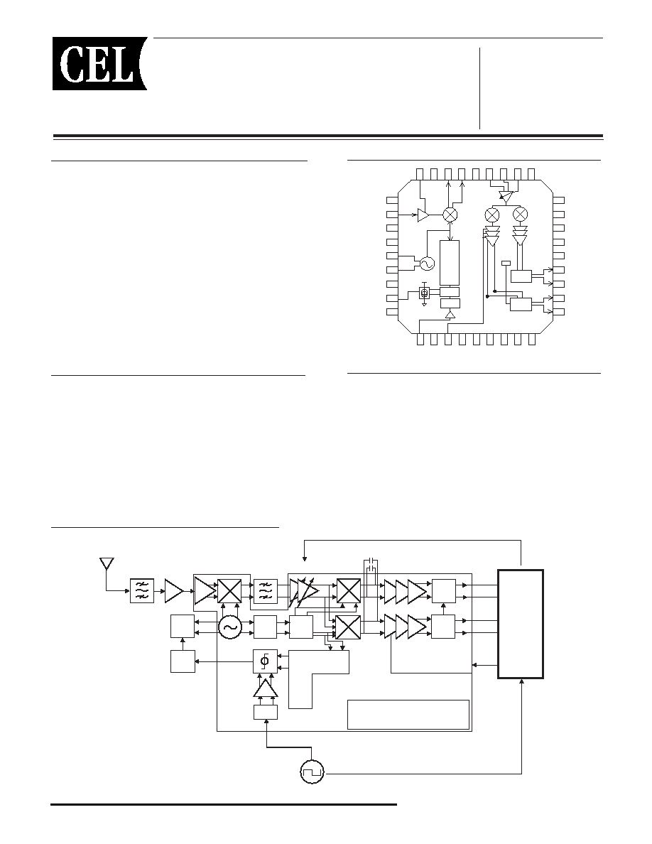
BLOCK DIAGRAM
∑ LOW POWER CONSUMPTION: 52 mW
∑ DUAL-CONVERSION IQ DOWN CONVERTER
1
:
Reference frequency: REF
in
= 27 MHz
∑ PSEUDO-BASEBAND WITH 2-BIT DIGITIZED OUTPUT
∑ ON-CHIP LNA, ON-CHIP FREQUENCY SYNTHESIZER,
IF AGC AMPLIFIER:
with 45 dB typical range of adjustable gain
∑ SMALL 36 PIN QFN PACKAGE:
Flat lead style for better RF performance
Note:
1. Based on eRide's proprietary GPS DSP architecture
California Eastern Laboratories
APPLICATIONS
∑ E911 ENABLED MOBILE PHONE
∑ IN-VEHICLE NAVIGATION SYSTEMS
∑ LOW POWER HANDHELD GPS RECEIVER
∑ PC/PDA+GPS INTEGRATION
∑ ASSET TRACKING
UPB1008K
1stMIX
LNA
PIN 1 ≠
OSC
PD
1/2
Dividers
IQ DEMO
AGC
ADC
ADC
DESCRIPTION
NEC's UPB1008K is a Silicon RFIC especially designed for
handheld low power/low cost GPS receivers. The IC com-
bines an LNA, followed by a double-conversion RF/IF
downconverter block and a PLL frequency synthesizer on one
chip. The second IF Freqency is a pseudo- baseband signal
into a on-chip 2-bit A/D converters.The device can operate on
a supply voltage as low as 2.7 V, and is a housed in a small 36
pin QFN (Quad, Flat, No-lead) package, resulting in a very low
power consumption and reduced board space.
NEC's stringent quality assurance and test procedures en-
sure the highest reliability and performance.
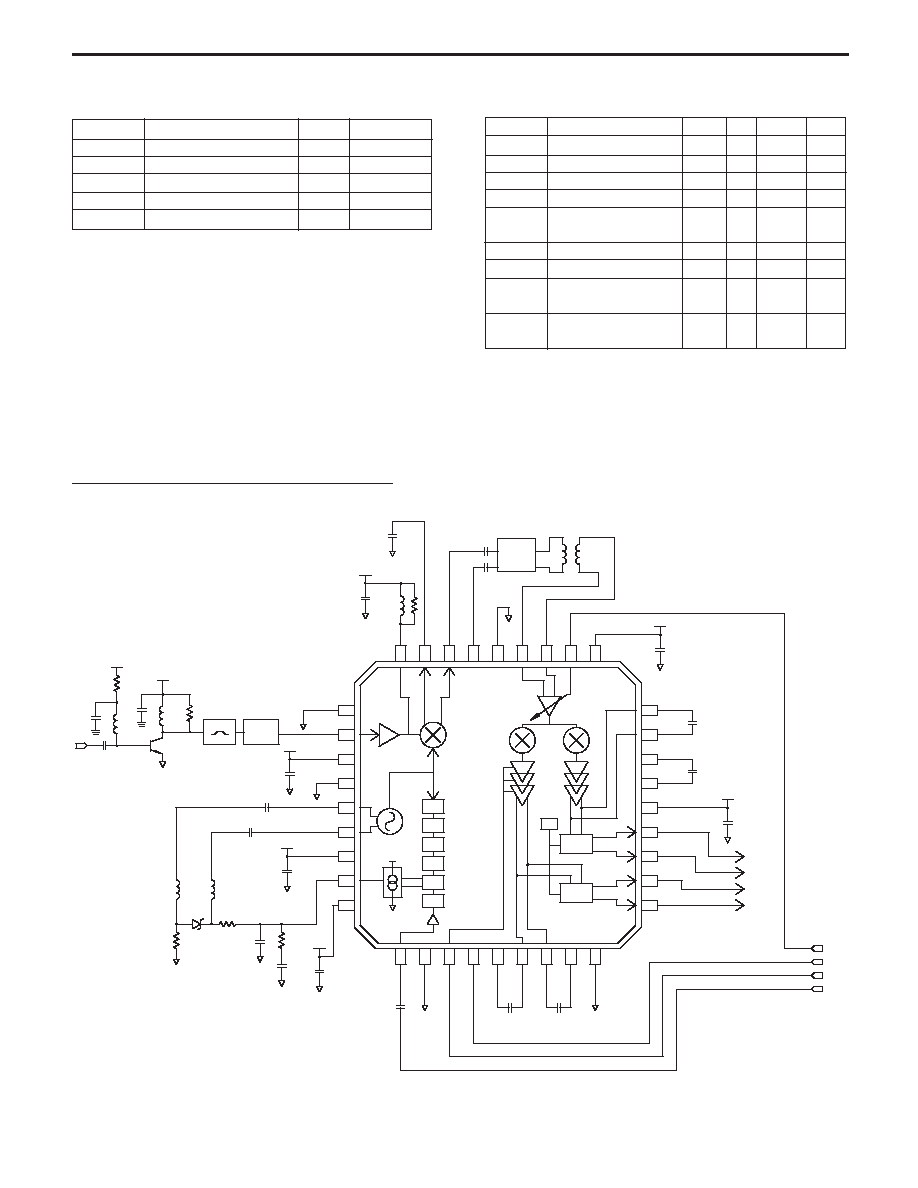
RF APPLICATION DIAGRAM
ISign
IMag
QSign
QMag
2-bit
ADC
2-bit
ADC
REFin
27 MHz
Reference
Clock
Regulator Circuitry
PLL Frequency
Counters
/2
/6
/7
/8
/2
/2
/4
TANK
Loop
Filter
IF filter
AGC
LNA
1st Mixer
RF SAW
BASEBAND I
C
Nyquist Filters
I/Q
Balance

UPB1008K
ADVANCED GPS COMPLETE SOLUTION
e911
AUTOMOTIVE
eYELLOW PAGES
PERSONAL GPS
ASSET
TRACKING
NETWORK
TRACKING
P L L
A D C
OPUS
STATE
MACHINE
ACQUISITION
TEMP
TIME
FREQ
GAIN
CONTROL
TRACKING
A D C
eRide NAVIGATION
SOFTWARE & DRIVERS
eRide
SMART SERVER
eRide WORLDWIDE
REFERENCE STATION
NETWORK
U P B 1 0 0 8 K
O p u s 1
UART
ADVANCED GPS COMPLETE SOLUTION
"NEC Corporation and eRide, Inc. have teamed to provide an advanced positioning solution delivering high GPS performance,
accuracy, integration and architecture flexibility. The chip set combines CEL's UPB1008K receiver IC with eRide's Opus One SOC
(System-on-a-Chip) Baseband ASIC and is suitable for standard GPS products as well as Cellular Handset applications. Also provided
are scalable client navigation software and drivers, plus location-aiding data from eRide's Smart Server. Together, they offer a
complete hardware/infrastructure solution.
The chip set's design allows it to operate independently of wireless interface standards - and independently of the host product's CPU
and Operating System. This unique approach to system integration makes it easy to deploy the chip set into an wireless application,
in any wireless network. A "Universal Hardware" solution, the design promises lower manufacturing costs and, ultimately lower cost
to the consumer.
The chip set's advanced positioning architecture offers unmatched sensitivity providing fast, accurate positioning architecture offers
unmatched sensitivity providing fast and accurate position fixes, even when indoors or in deep in urban canyons."
POWER DISSIPATION
First Fix
400 mW
Tracking
200-300 mW
Stand By
30 mW
HIGH PERFORMANCE GPS OMNI MODE
LI, C/A code receiver
Performance
Indoor
Outdoor
Time to First Fix w/ aiding
5-7sec
1-3sec
Time to First Fix w/o aiding
10-20sec
3-5sec
Accuracy
10-25m cep
2-5m cep
Sensitivity
-155dBm
-142dBm
in 1sec dwells
in two 10msec dwells
Superior performance in high reflection indoor environments and in urban canyon types of outdoor environments
UPB1008K
LNA/RF DOWNCONVERTER
(f
RFin
= 1575.42 MHz, f
1stLOin
= 1400 MHz, P
LO
= -10 dBm, f
1stIF
= 175 MHz, Pin 13: V
IL
= 3 V, Z
L
differential = 32 & Z
S
= opt)
CG
LNA_MIX
Power conversion gain from 2nd LNA/mixer to 1st IF,
dB
18
23
28
P
RFin
= -50 dBm
NF
LNA_MIX
Noise Figure of 2nd LNA/mixer(SSB), Input matched
dB
≠
5
≠
P
1dBLNA_MIX
1 dB Compression refer to source, Input matched
dBm
≠
-38
≠
Z
LNAin
RF Input Impedance of LNA
Ohm
≠
31
≠
Z
MIXout
IF Output Impedance of Mixer
Ohm
32
A
LO-IF
Local Signal Leak to IF, f
1stLOin
=1400 MHz,
dBm
≠
-35
≠
P
LO
= 0 dBm
A
LO-RF
Local Signal Leak to RF, f
1stLOin
=1400 MHz,
dBm
≠
-50
≠
P
LO
= 0 dBm
PLL
I
CPOH
PLL Charge Pump High Side Current @ V
CPout
= V
CC/
2
µA
≠
200
≠
I
CPOL
PLL Charge Pump Low Side Current @ V
CPout
= V
CC/
2
µA
≠
-200
≠
f
PD
Phase Comparison Frequency
MHz
≠
13.5
≠
CRYSTAL OSCILLATOR/REVERENCE AMPLIFIER BLOCK
V
REFin
Reference input minimum level
mVpp
50
200
≠
f
REF
Input Frequency of Reference Input
MHz
≠
27
≠
VT
VCO Control Voltage, PLL Locked
V
0.8
1.5
2.2
C/N
VCO C/N, 1kHz, Loop band width = 5 kHz
dBc/Hz
57
62
≠
AGC AMPLIFIER, I-Q DEMODULATOR, and ADC BLOCK(f
1stIFin
= 175 MHz, Z
in
= 600)
CG
AGC/MIX
Maximum voltage conversion gain of AGC amplifier/
dB
≠
30
≠
I-Q mixer, P
in
= -60 dBm, V
AGC
= 0.5 V, Unmatched
Minimum voltage conversion gain of AGC amplifier/
dB
≠
-15
≠
I-Q mixer, P
in
= -60 dBm, V
AGC
= 2.0 V, Unmatched
A
AGC/MIX
AGC control range, V
AGC
= 0.5 V to 2 V
dB
25
45
≠
P
1dBAGC
1 dB compression input to AGC amplifier,
dBm
≠
-45
≠
set voltage gain = 30 dB
V
AGC
AGC control voltage
V
0.5
≠
2.0
BW
3dB Mixer Bandwidth
MHz
≠
10
≠
V
IQ-C
IQ BalanceControl Voltage, Gain(Ich) = Gain (Qch)
V
≠
2.1
2.8
A
IQ-C
IQ Balance Control Gain Range, V
IQ-C
= 0 to 3 V
dB
4.0
6.5
≠
Duty
Ich Mag Bit Output Pulse Duty, P1stIFin = -84 dBm
%
50
≠
≠
Ich
V
AGC
= 0.5 V, V
IQ-C
= 0 V
Duty
Qch Mag Bit Output Pulse Duty, PIF2in = -88 dBm
%
50
≠
≠
Qch
V
AGC
= 0.5 V, V
IQ-C
= 0 V
BASEBAND AMPLIFIER BLOCK (Z
S
= 2k & Z
L
= 2 k)
V
BBOH
Baseband output logic high, C
L
= 10 pF
V
2.0
≠
≠
V
BBOL
Baseband output logic low, C
L
= 10 pF
V
0
≠
0.5
SYMBOLS
PARAMETERS AND CONDITIONS
UNITS
MIN
TYP
MAX
SYMBOLS
PARAMETERS AND CONDITIONS
UNITS
MIN
TYP
MAX
SYMBOLS
PARAMETERS AND CONDITIONS
UNITS
MIN
TYP
MAX
SYMBOLS
PARAMETERS AND CONDITIONS
UNITS
MIN
TYP
MAX
SYMBOLS
PARAMETERS AND CONDITIONS
UNITS
MIN
TYP
MAX
SYMBOLS
PARAMETERS AND CONDITIONS
UNITS
MIN
TYP
MAX
I
CC
Total Circuit Current, No Signals
mA
14
18
23.5
V
CC
Supply Voltage
V
2.7
3.0
3.3
I
CC_PD
Power down current, PIN 13 = V
IL
µA
≠
1
10
I
CC
rf
RF Block Circuit Current (pin 3), No signal
µA
0.4
0.5
0.7
I
CC
lo
VCO Block Circuit Current (pin 7), No signal
mA
4.1
5.6
7.2
ICC pll
PLL Block Circuit Current (pin 9), No signal
mA
2.7
3.6
4.7
ICC bb
Baseband Block Circuit Current (pin 23), No signal,
mA
2.5
3.4
4.3
open load
ICC if
IF Block Circuit Current (pin 28) , No signal
mA
2.7
3.7
4.7
ICC lna
Pre-Amplifier Open Connector Current (pin 36),
mA
1.0
1.4
1.8
No signal
ELECTRICAL CHARACTERISTICS
(T
A
= 25∞C, V
CC
= 3.0 V, unless otherwise specified)
APPLICATION CIRCUIT
ABSOLUTE MAXIMUM RATINGS
1,2
(T
A
= 25∞C)
Notes:
1. Operation in excess of any one of these parameters may result
in permanent damage.
2. More than two items must not be reached simultaneously.
3. T
A
= +85∞C, mounted on a 50 x 50 x 1.6 mm double-sided
copper clad epoxy glass PWB.
4. T
A
= 25∞C
SYMBOLS
PARAMETERS
UNITS MIN
TYP
MAX
V
CC
Supply Voltage
V
2.7
3.0
3.3
T
OP
Operating Temperature
∞C
-40
+25
+85
f
RFin
RF Input Frequency
MHz
1575
f
REFin
Reference Frequency
MHz
27
f
1st
LO
1st LO Oscillating
Frequency
MHz
1400
f
1stIFin
1st IF Input Frequency
MHz
175
f
2ndLOin
2nd LO Input Frequency MHz
175
V
IH
Power Down Control
Voltage "High"
V
2
V
CC
V
IL
Power Down Control
Voltage "Low"
V
0
0.5
RECOMMENDED
OPERATING CONDITIONS
SYMBOLS
PARAMETERS
UNITS
RATINGS
V
CC
Supply Voltage
4
V
CC
3.6
P
D
Total Power Dissipation
3
mW
361
T
OP
Operating Temperature
∞C
-40 to +85
T
STG
Storage Temperature
∞C
-55 to +150
I
CC_total
Total Circuit Current
4
UPB1008K
1
2
3
4
5
6
7
8
9
10
11
12
13
14
15
16
17
18
19
20
21
22
23
24
25
26
27
28
29
30
31
32
33
34
35
36
SAW
FILTER
12pF
6.8nH
12pF
NE662MO4
2Bit ADC
2Bit ADC
Vth
1/2
1/6.375
1/4
1/2
1/2
PD
CP
OSC
LNA
1stMIX
AGC
IQ_DEMO
150pF
21FoutI
21Foutb
100nF
DCoffsetI
DCoffsetb
100nF
VCC
I_mag
I_sign
Q_sign
Q_mag
VCCbb
I_mag
I_sign
Q_sign
Q_mag
1OOnF
DCoffsetQ
GNDbb
150pF
21FoutQ
21FoutQb
GNDdig
100nF
Refin
Ic_cntl
PD
DCoffsetQb
Vagc
ic_cntl
REFin
PD
15pF
VCC
1.2nH
0.1uF
100nF
VCC
1:16
SAW
IN
INb
OUTb
OUT
15pF
GNDanalog
VCCanalog
VAGC
IFin2
IFin1
Mixout2
Mixout1
Vref
LNAbias
100nF
VCC
1.2K
3.3nH
0.01uF
22pF
15K
3.3nH
15K
VCC
100nH
12pF
12pF
D0
100nF
VCC
43K
RF_in
.1pF
3.3nH
VCC
VCC
NETWORK
MATCHING
GND1na
LNAin
GNDIo
VCCrf
1stLO-OSC1
VCCIo
PDout
1stLO-OSC2
Vccdig
uPB1008K
0.1uF
200
300
Pin No.
Symbol
Function and Application
Internal Equivalent Circuit
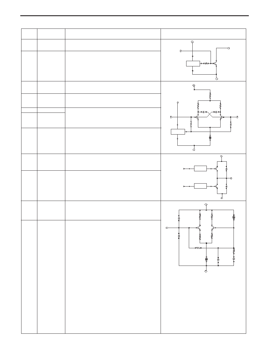
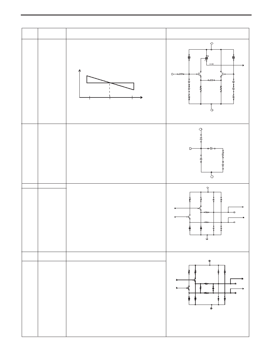
1
GNDlna
Ground pin of LNA
2
LNAin
Input pin of low noise amplifier. It is a
single-ended open collector design.
Capacitive coupling is required; external
matching will improve gain or NF.
3
VCCrf
Supply voltage pin of LNA, RF mixer and VCO
voltage regulator.
4
GNDlo
Ground pin of 1st LO Oscillator circuit and RF
Mixer.
5
1stLO-OSC1
Pin 5 & 6 are base pins of the differential
6
1stLO-OSC2
amplifier for 1st LO oscillator. These pins
require an LC (varacator) tank circuit to
oscillate at around 1400 MHz.
7
VCClo
Supply voltage pin of oscillator circuit for
1st LO Oscillator and RF mixer
8
PDout
This is a current mode charge pump output.
For connection to a passive RC loop filter for driving
external varactor diode of 1stLO-OSC.
9
VCCdig
Supply voltage pin of digital portion of the chip.
10
REFin
Input pin of reference frequency buffer. This pin
should be equipped with external 27 MHz
oscillator (e.g. TCXO).
11
GNDdig
Ground pin of digital portion of the chip.
PIN FUNCTIONS
UPB1008K
B
ias
V
CC
Regulator
r=6.5k
GND
1
3
2
36
r = 410
c=1.8p
c=1.8p
r=4.4k
V
CC
Regulator
GND
6
r=4.4k
7
5
idc=941u
4
r=300
r=300
Bias
3
Source
Source Control
PFD
PFD
FROM PFD
Sink Control
Sink
ESD
ESD
9
8
11
9
r=20k
r=20k
r=500
r=50k
r=500
ESD
ESD
r=30k
c=5.4p
idc=22u
10
idc=9.7u
11
Pin No.
Symbol
Function and Application
Internal Equivalent Circuit
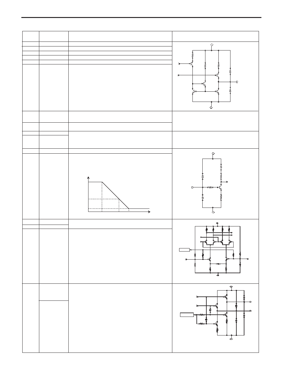
12
I/Q Balance
The voltage on this pin controls the Q channel
Control
IF Amplifier Gain. Gain control of ±2 dB can be
achieved for 0~3 V.
Leave open-circuited if not used.
13
PD1
Standby mode control.
Low=whole chip OFF & High=Whole chip ON.
14
2IFout-Q
Differential ouptut pins of quadrature demodulator
15
2IFout-Qb
Q output. Adding a lowpass shunt capacitor
between these pins will define the IF Bandwidth.
16
DC offset Q
DC offset compensation pin for C arm. A low pass
capacitor shunt to Pin 17 is required.
17
DC offset Qb
DC offset compensation pin for Q-bar arm.
A low pass capacitor shunt to Pin 16 is required.
PIN FUNCTIONS
UPB1008K
28
32
r=200k
r=7.1k
r=7.1k
r=7.1k
r=7.1k
idc=23.5u
idc=23.5u
Iref
CCCS
r=12k
12
r=28k
11
13
V
CC
ESD
ESD
r=2k
r=2k
r=2k
r=2k
ESD
ESD
28
15,(26)
14,(27)
T
o
channel amp
ESD
ESD
idc=86u
idc=86u
From 2nd Mixer
32
28
r=4k
r=4k
ESD
ESD
ESD
ESD
From 2nd Mixer
idc=84u
idc=84u
r=20k
r=150k
r=150k
32
16,(25)
17,(24)
T
o
of
fset amp
c=9p
Qgain
0 V
1.5 V
3 V
V
≠2dB
+2dB
Pin No.
Symbol
Function and Application
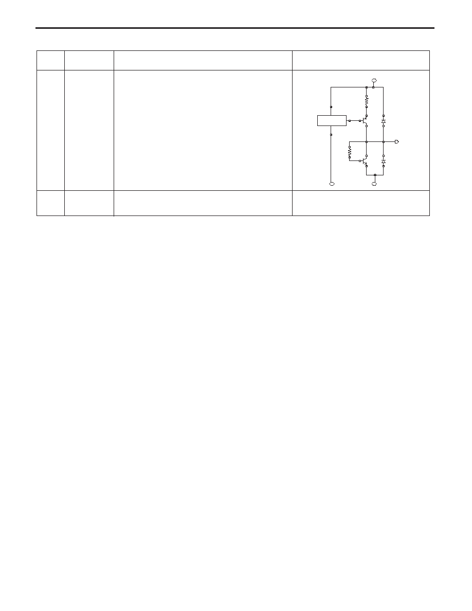
Internal Equivalent Circuit
18
GNDbb
Ground pin of CMOS output driver.
19
Qmag
Digitized Q signal. Magnitude bit of 2-bit ADC output.
20
Qsign
Digitized Q signal. Sign bit of 2-bit ADC output
21
Isign
Digitized I signal. Sign bit of 2-bit ADC output.
22
Imag
Digitized I signal. Magnitude bit of 2-bit ADC output.
23
VCCbb
Supply voltage pin of CMOS output driver.
24
DCoffsetIb
DC offset compensation pin for I-bar arm.
See pin 16 & 17 schematic
A low pass capacitor shunt to Pin 25 is required.
25
DCoffsetI
DC offset compensation pin for I arm.
A low pass capacitor shunt to Pin 24 is required.
26
2IFout-Ib
Differential output pins of quadrature
See pin 14 & 15 schematic
27
2IFout-I
demodulator I output. Adding a lowpass shunt
capacitor between these pins will define the
IF bandwidth.
28
VCC if
Supply voltage pin of analog portion of the chip.
29
V
AGC
Gain control voltage pin of IF amplifier. This voltage
performs reverse control,(i.e., V
AGC
up
gain down).
If this pin is left open, then it is default at
maximum gain.
30
IF-in1
Differential input pins of 1st IF AGC amplifier
31
IF-in2
32
GNDanalog
Ground pin of analog portion of the chip.
33
Mixout2
Differential output pins of RF mixer. This is an emitter
34
Mixout1
follower output buffer, provide a 50 output load.
PIN FUNCTIONS
UPB1008K
19, (20,21,22)
r=21.5
r=5k
r=21.5
From Comparator
23
18
ESD
ESD
ESD
ESD
r=3k
To AGC Amp
r=300
28
29
32
r=44k
Regulator
Bias
30
ESD
ESD
ESD
ESD
r=4k
r=4k
r=2k
r=2k
r=4k
r=4k
r=1.42k
r=1.42k
r=40
28
From V
AGC
AGC amp out
31
32
7
ESD
ESD
ESD
ESD
r=111
r=111
From Mixer
34
33
4
Regulator
r=4k
r=4k
c=1.67p
c=1.67p
30
0
-15
0.5
1.5
2
V
AGC
(V)
Typical AGC
Gain Response
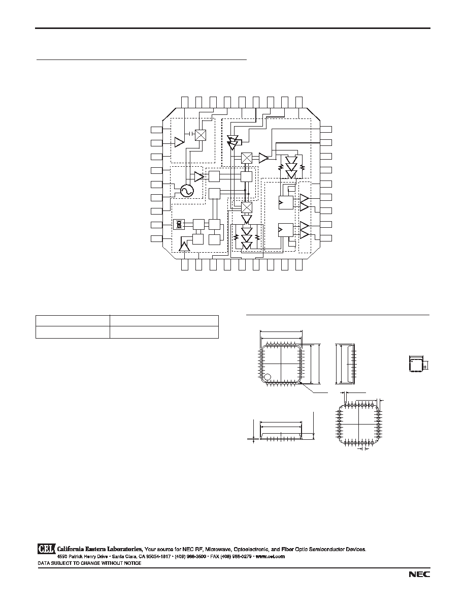
Pin No.
Symbol
Function and Application
Internal Equivalent Circuit
35
Vref
Base-emitter junction voltage wth respect to ground.
May be used for biasing an external discrete
transistor. Regulation will develop PTAT current.
36
LNAbias
LNA output pin. External bias (V
CC
) and matching
See pin 2 schematic
for gain is required.
PIN FUNCTIONS
UPB1008K
3
35
1
4
ESD
ESD
GND
VCC
r=40k
Regulator
r=500
Bias
UPB1008K
A Business Partner of NEC Compound Semiconductor Devices, Ltd.
05/27/04
Life Support Applications
These NEC products are not intended for use in life support devices, appliances, or systems where the malfunction of these products can reasonably
be expected to result in personal injury. The customers of CEL using or selling these products for use in such applications do so at their own risk and
agree to fully indemnify CEL for all damages resulting from such improper use or sale.
INTERNAL BLOCK DIAGRAM
27
26
25
23
24
22
21
20
19
1
2
3
5
4
6
7
8
9
35
33
30
28
34
31
29
32
36
11
13
16
18
12
15
17
14
10
2ndIFoutl
2ndIFoutlb
DCoffsetl
DCoffsetlb
V
CCbb
GNDbb
Imag
Isign
Qsign
Qmag
PDout
GNDdig
REF
in
I/Q Balance
PD
2IFoutQ
2IFoutQb
DCof
fsetQ
DCof
fsetQb
GND LNA
LNAin
V
CCrf
Mixout1
V
CCLO
GNDanalog
V
AGC
V
CC
if
IFin2
IFin1
GND
LO
1stLO-OSC1
1stLO-OSC2
V
CC
dig
LNA
bias
V
ref
Mixout2
/2
/2
PD
/6/7
8
/2
/4
2-bit
ADC
2-bit
ADC
V
th
V
th
Caution:
The island pins located on the corners are needed to fabricate
products in our plant, but do not serve any other function.
Consequently the island pins should not be soldered and should
remain non-connection pins.
OUTLINE DIMENSIONS
(Units in mm)
Package Outline QFN-36
Pin 1
Pin 36
4 -CO.5
6.2±0.2
6.0±0.2
6.0±0.2
6.2±0.2
6.2±0.2
6.0±0.2
6.2±0.2
0.14
+0.10
-0.05
6.0±0.2
1.0 MAX
0.55±0.2
0.22±0.05
0.5
Part Number
Package
UPB1008K-A
36 Pin plastic QFN
ORDERING INFORMATION
3.8
0.5
6.4
6.0
Actual size
4590 Patrick Henry Drive
Santa Clara, CA 95054-1817
Telephone: (408) 919-2500
Facsimile: (408) 988-0279
Subject: Compliance with EU Directives
CEL certifies, to its knowledge, that semiconductor and laser products detailed below are compliant
with the requirements of European Union (EU) Directive 2002/95/EC Restriction on Use of Hazardous
Substances in electrical and electronic equipment (RoHS) and the requirements of EU Directive
2003/11/EC Restriction on Penta and Octa BDE.
CEL Pb-free products have the same base part number with a suffix added. The suffix ≠A indicates
that the device is Pb-free. The ≠AZ suffix is used to designate devices containing Pb which are
exempted from the requirement of RoHS directive (*). In all cases the devices have Pb-free terminals.
All devices with these suffixes meet the requirements of the RoHS directive.
This status is based on CEL's understanding of the EU Directives and knowledge of the materials that
go into its products as of the date of disclosure of this information.
Restricted Substance
per RoHS
Concentration Limit per RoHS
(values are not yet fixed)
Concentration contained
in CEL devices
-A
-AZ
Lead (Pb)
< 1000 PPM
Not Detected
(*)
Mercury
< 1000 PPM
Not Detected
Cadmium
< 100 PPM
Not Detected
Hexavalent Chromium
< 1000 PPM
Not Detected
PBB
< 1000 PPM
Not Detected
PBDE
< 1000 PPM
Not Detected
If you should have any additional questions regarding our devices and compliance to environmental
standards, please do not hesitate to contact your local representative.
Important Information and Disclaimer: Information provided by CEL on its website or in other communications concerting the substance
content of its products represents knowledge and belief as of the date that it is provided. CEL bases its knowledge and belief on information
provided by third parties and makes no representation or warranty as to the accuracy of such information. Efforts are underway to better
integrate information from third parties. CEL has taken and continues to take reasonable steps to provide representative and accurate
information but may not have conducted destructive testing or chemical analysis on incoming materials and chemicals. CEL and CEL
suppliers consider certain information to be proprietary, and thus CAS numbers and other limited information may not be available for
release.
In no event shall CEL's liability arising out of such information exceed the total purchase price of the CEL part(s) at issue sold by CEL to
customer on an annual basis.
See CEL Terms and Conditions for additional clarification of warranties and liability.