DESCRIPTION
The
PC8231TK is a silicon germanium carbon (SiGe:C) monolithic integrated circuit designed as low noise
amplifier for GPS and mobile communications. This device exhibits low noise figure and high power gain
characteristics. This device is enabled in the frequency range from 1.5 to 2.4 GHz by modifying the external matching
circuit.
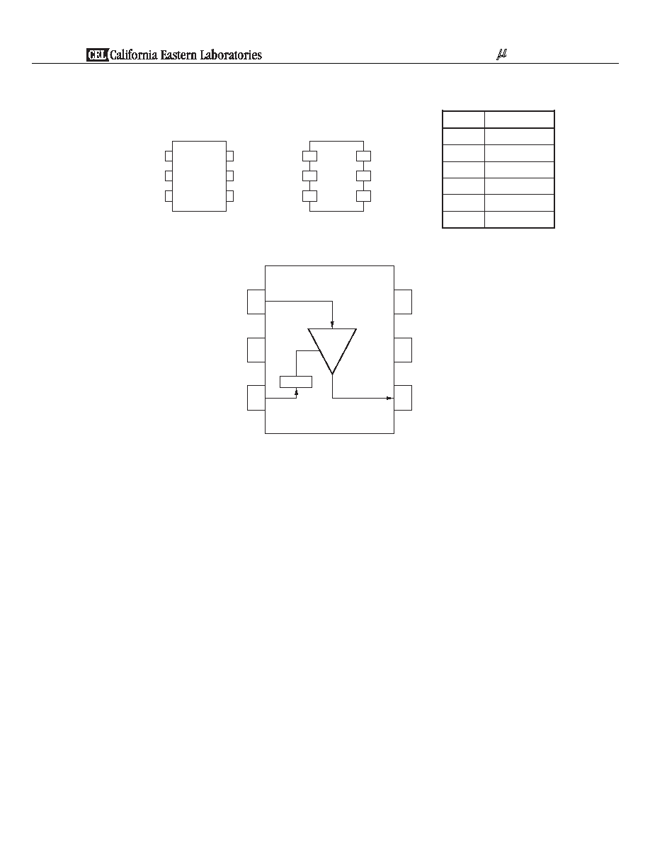
The package is 6-pin lead-less minimold, suitable for surface mount.
This IC is manufactured using our UHS4 (Ultra High Speed Process) SiGe:C bipolar process.
FEATURES
f
@
.
P
Y
T
B
d
8
.
0
=
F
N
:
e
s
i
o
n
w
o
L
∑
in
= 1 575 MHz
G
:
n
i
a
g
h
g
i
H
∑
P
= 20 dB TYP. @ f
in
= 1 575 MHz
∑ Low current consumption
: I
CC
= 3.8 mA TYP. @ V
CC
= 3.0 V
∑ Built-in power-saving function
∑ High-density surface mounting
: 6-pin lead-less minimold package (1.5
1.1
0.55 mm)
∑ Included very robust bandgap regulator (Small V
CC
and T
A
dependence)
∑ Included protection circuits for ESD
APPLICATION
∑ Low noise amplifier for GPS and mobile communications
ORDERING INFORMATION
Part Number
Order Number
Package
Marking
Supplying Form
PC8231TK-E2
PC8231TK-E2-A
6-pin lead-less minimold
(1511 PKG) (Pb-Free)
6K
∑ 8 mm wide embossed taping
∑ Pin 1, 6 face the perforation side of the tape
∑ Qty 5 kpcs/reel
Remark To order evaluation samples, contact your nearby sales office.
Part number for sample order: PC8231TK
DATA SHEET
Caution Observe precautions when handling because these devices are sensitive to electrostatic discharge.
BIPOLAR ANALOG INTEGRATED CIRCUIT
PC8231TK
SiGe:C LOW NOISE AMPLIFIER
FOR GPS/MOBILE COMMUNICATIONS
Document No. PU10613EJ01V0DS (1st edition)
Date Published April 2006 NS CP(N)
The information in this document is subject to change without notice. Before using this document, please confirm
that this is the latest version.
ABSOLUTE MAXIMUM RATINGS
t
i
n
U
s
g
n
i
t
a
R
s
n
o
i
t
i
d
n
o
C
t
s
e
T
l
o
b
m
y
S
r
e
t
e
m
a
r
a
P
V
e
g
a
t
l
o
V
y
l
p
p
u
S
CC
T
A
= +25
V
0
.
4
C
Power-Saving Voltage
V
PS
T
A
= +25
V
0
.
4
C
P
n
o
i
t
a
p
i
s
s
i
D
r
e
w
o
P
D
T
A
= +85∞C
Note
232
mW
Operating Ambient Temperature
T
A
40 to +85
C
Storage Temperature
T
stg
55 to +150
C
P
r
e
w
o
P
t
u
p
n
I
in
m
B
d
0
1
+
Note Mounted on double-side copper-clad 50
50
1.6 mm epoxy glass PWB
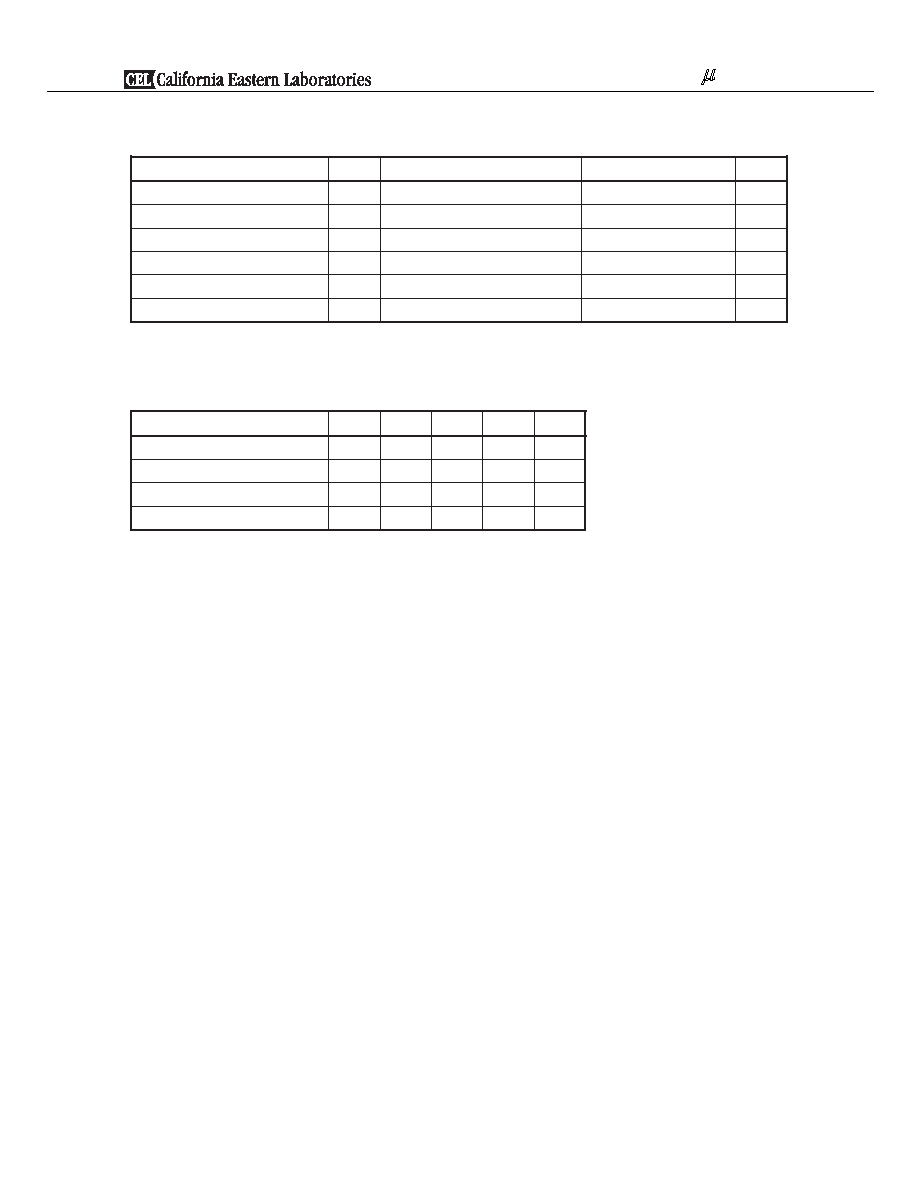
RECOMMENDED OPERATING RANGE
Parameter
Symbol
MIN.
TYP.
MAX.
Unit
V
e
g
a
t
l
o
V
y
l
p
p
u
S
CC
2.7
3.0
3.3
V
Operating Ambient Temperature
T
A
40
+25
+85
C
Power Save Turn-on Voltage
V
PSon
1.6
V
CC
V
Power Save Turn-off Voltage
V
PSoff
0
0.4
V
Data Sheet PU10613EJ01V0DS
3
PC8231TK
ELECTRICAL CHARACTERISTICS
(T
A
= +25 C, V
CC
= V
PS
= 3.0 V, f
in
= 1 575 MHz, unless otherwise specified)
Parameter
Symbol
Test Conditions
MIN.
TYP.
MAX.
Unit
I
t
n
e
r
r
u
C
t
i
u
c
r
i
C
CC
No Signal (V
PS
= 3.0 V)
2.8
3.8
5.1
mA
V
(
e
d
o
M
g
n
i
v
a
S
-
r
e
w
o
P
t
A
PS
= 0 V)
1
A
G
n
i
a
G
r
e
w
o
P
P
P
in
=
B
d
5
.
2
2
0
2
5
.
7
1
m
B
d
5
3
F
N
e
r
u
g
i
F
e
s
i
o
N
0.8
1.1
dB
Input 3rd Order Distortion Intercept
Point
IIP
3
f
in
1 = 1 574 MHz, f
in
2 = 1 575 MHz
10
dBm
L
R
s
s
o
L
n
r
u
t
e
R
t
u
p
n
I
in
0
1
7
dB
Output Return Loss
RL
out
8
1
0
1
dB
L
S
I
n
o
i
t
a
l
o
s
I
35
dB
Gain 1 dB Compression Input Power
P
in (1 dB)
22
dBm
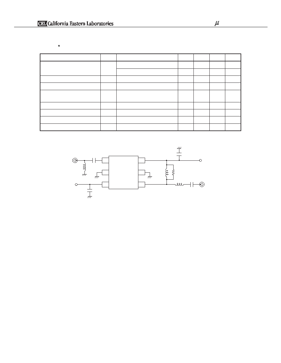
TEST CIRCUIT
100 pF
6
1
2
3
5
4
100 pF
0.1 F
8.2 nH
INPUT
OUTPUT
1 000 pF
470
18 nH
4.7 nH
V
PS
V
CC
Data Sheet PU10613EJ01V0DS
4
PC8231TK

TYPICAL CHARACTERISTICS (T
A
= +25 C, unless otherwise specified)
6
5
4
3
2
0
2.0
3.0
4.0
1
2.5
3.5
6
5
4
3
2
0
0
1.0
3.0
1
0.5
1.5
2.0
2.5
24
22
20
18
16
14
1 500
1 550
1 600
1 525
1 575
V
CC
= V
PS
RF = off
V
CC
= 3 V
RF = off
V
CC
= V
PS
= 3 V
1.6
1.4
1.2
0.8
0.6
0
1 500
1 550
1 600
1 525
1 575
V
CC
= V
PS
= 3 V
1.0
0.4
0.2
24
22
20
18
16
14
≠50
25
100
≠25
75
V
CC
= V
PS
= 3 V
f
in
= 1 575 MHz
0
50
1.6
1.4
1.2
0.8
0.6
0
V
CC
= V
PS
= 3 V
f
in
= 1 575 MHz
1.0
0.4
0.2
≠50
25
100
≠25
75
0
50
T
A
= +85 C
≠40 C
+25 C
T
A
= +85 C
≠40 C
+25 C
T
A
= ≠40 C
+85 C
+25 C
T
A
= +85 C
≠40 C
+25 C
CIRCUIT CURRENT vs. SUPPLY VOLTAGE
Circuit Current I
CC
(mA)
Supply Voltage V
CC
(V)
Circuit Current I
CC
(mA)
CIRCUIT CURRENT vs.
POWER-SAVING VOLTAGE
Power-Saving Voltage V
PS
(V)
Power Gain G
P
(dB)
Frequency f
in
(MHz)
POWER GAIN vs. FREQUENCY
Noise Figure NF (dB)
Frequency f
in
(MHz)
NOISE FIGURE vs. FREQUENCY
Power Gain G
P
(dB)
Operating Ambient Temperature T
A
( C)
POWER GAIN vs. OPERATING
AMBIENT TEMPERATURE
NOISE FIGURE vs. OPERATING
AMBIENT TEMPERATURE
Operating Ambient Temperature T
A
( C)
Noise Figure NF (dB)
Remark The graphs indicate nominal characteristics.
Data Sheet PU10613EJ01V0DS
5
PC8231TK