Central
Semiconductor Corp.
TM
145 Adams Avenue
Hauppauge, NY 11788 USA
Tel: (631) 435-1110
Fax: (631) 435-1824
www.centralsemi.com
PROCESS
CP223
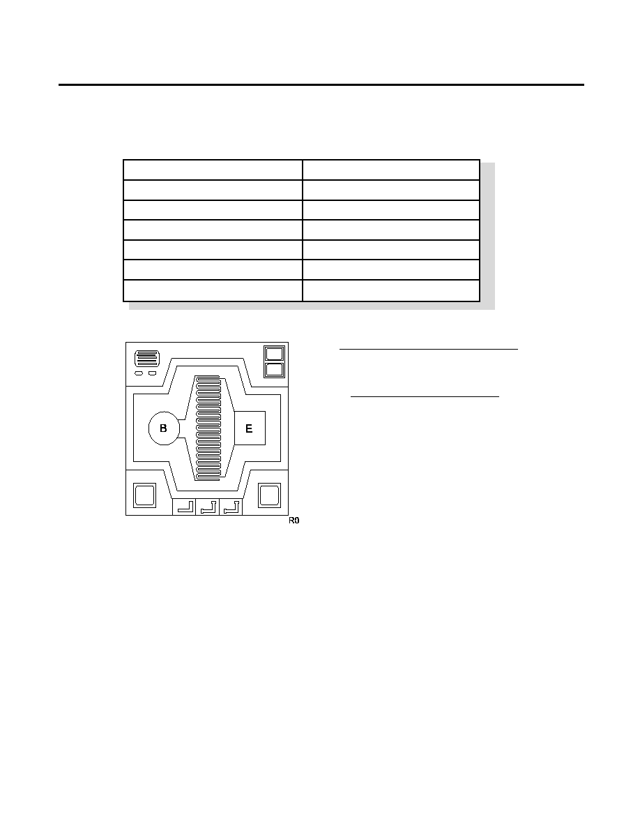
Small Signal Transistor
NPN - RF Transistor Chip
PRINCIPAL DEVICE TYPES
2N3866
GEOMETRY
PROCESS DETAILS
BACKSIDE COLLECTOR
R1 (1-August 2002)
Process
EPITAXIAL PLANAR
Die Size
22 x 22 MILS
Die Thickness
8.0 MILS
Base Bonding Pad Area
3.5 MILS DIAMETER
Emitter Bonding Pad Area
3.5 x 3.5 MILS
Top Side Metalization
Al - 30,000≈
Back Side Metalization
Au - 12,000≈
GROSS DIE PER 4 INCH WAFER
23,340
Central
Semiconductor Corp.
TM
Central
Semiconductor Corp.
TM
PROCESS
CP223
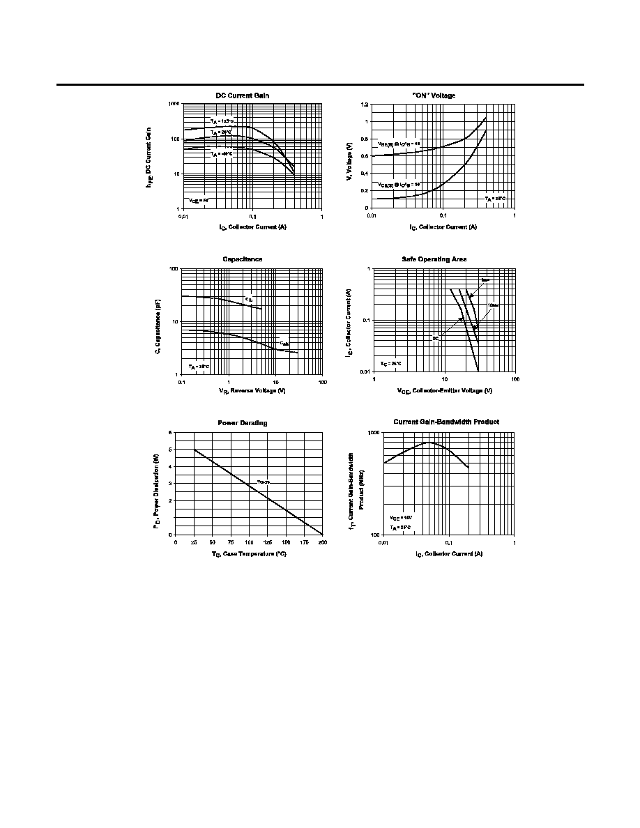
Typical Electrical Characteristics
145 Adams Avenue
Hauppauge, NY 11788 USA
Tel: (631) 435-1110
Fax: (631) 435-1824
www.centralsemi.com
R1 (1-August 2002)
Central
Semiconductor Corp.
TM