145 Adams Avenue
Hauppauge, NY 11788 USA
Tel: (631) 435-1110
Fax: (631) 435-1824
www.centralsemi.com
PRINCIPAL DEVICE TYPES
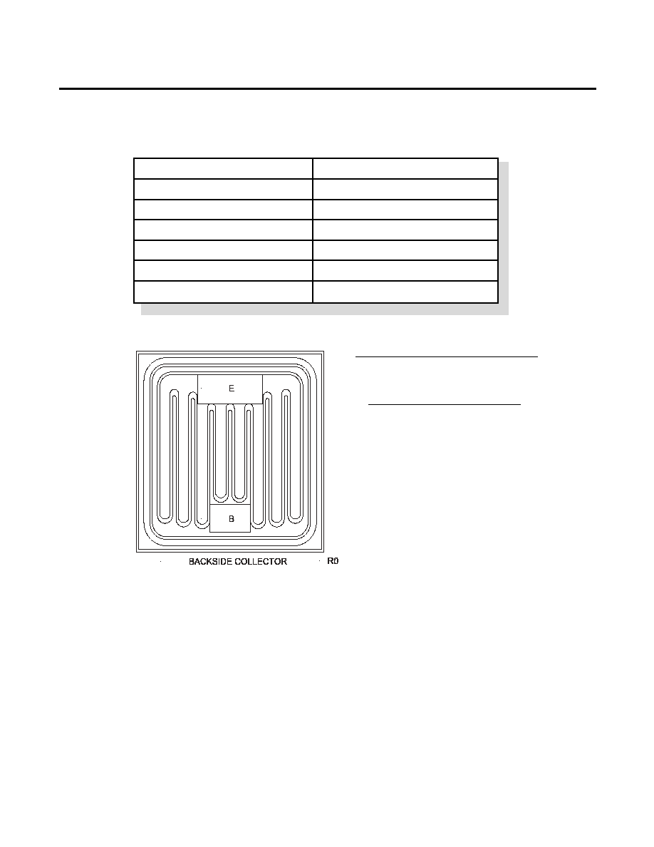
CJDD3110
GEOMETRY
PROCESS DETAILS
R2 (15- September 2003)
Process
EPITAXIAL PLANAR
Die Size
109.5 x 109.5 MILS
Die Thickness
9.0 MILS
Base Bonding Pad Area
23.6 x 15.4 MILS
Emitter Bonding Pad Area
37.8 x 15.8 MILS
Top Side Metalization
Al - 30,000≈
Back Side Metalization
Ti / Ni / Ag - 11,300≈
GROSS DIE PER 4 INCH WAFER
900
Central
Semiconductor Corp.
TM
PROCESS
CP311
Power Transistor
NPN High Voltage Transistor Chip
Central
Semiconductor Corp.
TM
PROCESS
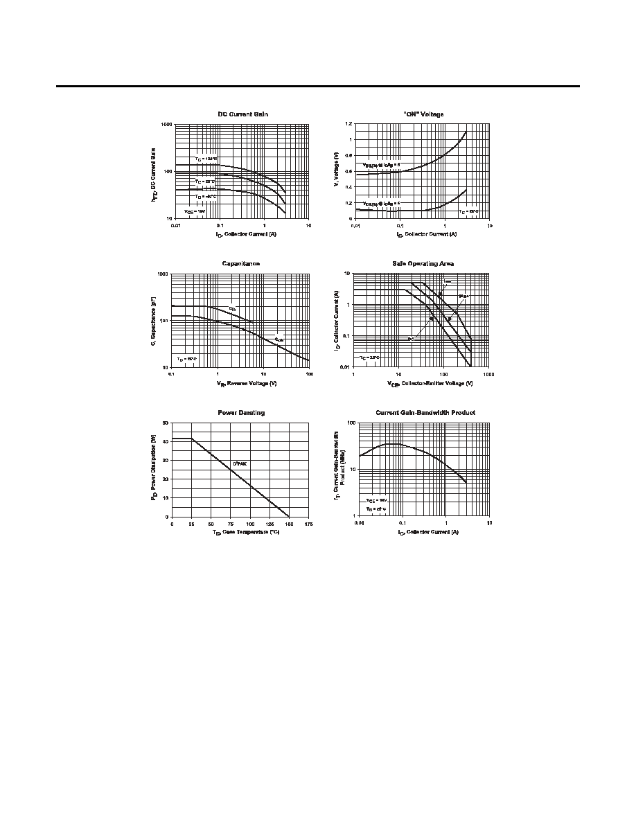
CP311
Typical Electrical Characteristics
145 Adams Avenue
Hauppauge, NY 11788 USA
Tel: (631) 435-1110
Fax: (631) 435-1824
www.centralsemi.com
R2 (15- September 2003)