 | –≠–ª–µ–∫—Ç—Ä–æ–Ω–Ω—ã–π –∫–æ–º–ø–æ–Ω–µ–Ω—Ç: 72SD3232 | –°–∫–∞—á–∞—Ç—å:  PDF PDF  ZIP ZIP |

1
M
e
m
o
r
y
All data sheets are subject to change without notice
(858) 503-3300 - Fax: (858) 503-3301 - www.maxwell.com
1 Gbit SDRAM
32-Meg X 32-Bit X 4-Banks
©2004 Maxwell Technologies
All rights reserved.
72SD3232
03.25.04 REV 1
F
EATURES
:
∑ 1 Gigabit ( 32-Meg X 32-Bit X 4-Banks)
∑ RAD-PAKÆ radiation-hardened against natural space
radiation
∑ Total Dose Hardness:
>100 krad (Si), depending upon space mission
∑ Excellent Single Event Effects:
SEL
TH
> 85 MeV/mg/cm
2
@
25
∞
C
∑ JEDEC Standard 3.3V Power Supply
∑ Clock Frequency: 100 MHz Operation
∑ Operating tremperature: -55 to +125
∞
C
∑ Auto Refresh
∑ Single pulsed RAS
∑ 2 Burst Sequence variations
Sequential (BL =1/2/4/8)
Interleave (BL = 1/2/4/8)
∑ Programmable CAS latency: 2/3
∑ Power Down and Clock Suspend Modes
∑ LVTTL Compatible Inputs and Outputs
∑ Package: 72-Pin R
AD
-Stack
Package
D
ESCRIPTION
:
Maxwell Technologies' Synchronous Dynamic Random
Access Memory (SDRAM) is ideally suited for space
applications requiring high performance computing and
high density memory storage. As microprocessors
increase in speed and demand for higher density mem-
ory escalates, SDRAM has proven to be the ultimate
solution by providing bit-counts up to 1 Gigabits and
speeds up to 100 Megahertz. SDRAMs represent a sig-
nificant advantage in memory technology over traditional
SRAMs including the ability to burst data synchronously
at high rates with automatic column-address generation,
the ability to interleave between banks masking pre-
charge time, and the ability to randomly change column
address during each clock cycle.
Maxwell Technologies' patented R
AD
-P
AK
Æ
packaging
technology incorporates radiation shielding in the micro-
circuit package. It eliminates the need for box shielding
for a lifetime in orbit or space mission. In a typical GEO
orbit, R
AD
-P
AK
Æ
provides greater than 100 krads(Si)
radiation dose tolerance. This product is available with
screening up to Class K.
Logic Diagram
(One Amplifier)

72SD3232
M
e
m
o
r
y
2
All data sheets are subject to change without notice
©2004 Maxwell Technologies
All rights reserved.
1 Gbit(32-Meg X 32-Bit X 4-Banks) SDRAM
03.25.04Rev 1
72SD3232
Pinout Description
Pin Descriptions
Pin Name
Function
A0 to A12
Address Input
BA0, BA1
Row Address A0 to A12
Column Address A0 to A9
Bank Select Address BA0/BA1 (BS)
DQ0 to DQ7
Data-Input/Output - Layer 1
DQ8 to DQ15
Data-Input/Output - Layer 2
DQ16 to DQ23
Data-Input/Output - Layer 3
DQ24 to DQ32
Data-Input/Output - Layer 4
CS\ Chip
Select
RAS\
Row Address Strobe
CAS\ Column
Address
Strobe
WE\
Write Enable
DQM 1
Input/Output Mask - Layer 1
DQM 2
Input/Output Mask - Layer 2
DQM 3
Input/Output Mask - Layer 3
DQM 4
Input/Output Mask - Layer 4
CLK1
Clock Input - Layer 1 & 3
CLK2
Clock Input - Layer 2 & 4
CKE
Clock Enable
Vcc
Power for internal circuits
Vss
Ground for internal circuits
VccQ
Power for DQ circuits
VssQ
Ground for DQ circuits
NC
No Connection
72SD3232
M
e
m
o
r
y
3
All data sheets are subject to change without notice
©2004 Maxwell Technologies
All rights reserved.
1 Gbit(32-Meg X 32-Bit X 4-Banks) SDRAM
03.25.04Rev 1
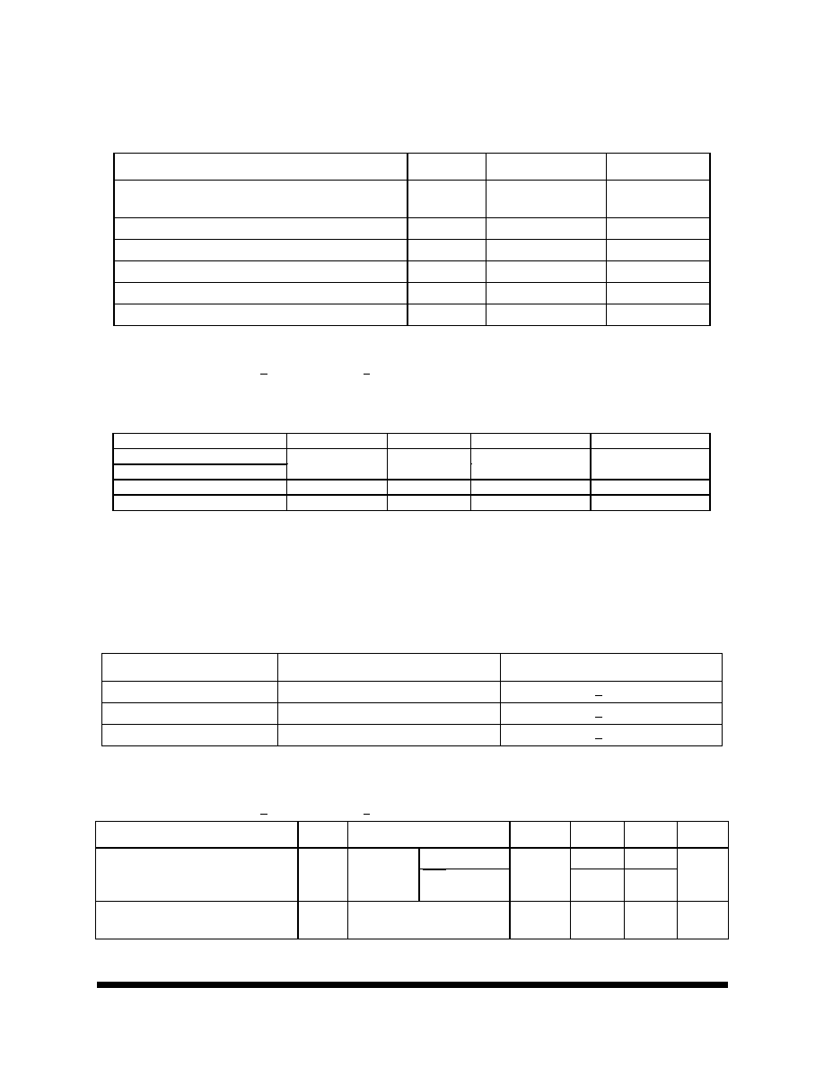
`
T
ABLE
1. A
BSOLUTE
M
AXIMUM
R
ATINGS
P
ARAMETER
S
YMBOL
M
AX
U
NIT
Voltage on any pin relative to V
SS
V
IN
V
OUT
-0.5 to VCC + 0.5
(< 4.6(max))
V
Supply voltage relative to V
SS
V
CC
-0.5 to +4.6
V
Short circuit output current
I
OUT
50
mA
Power Dissipation
P
D
1.0
W
Operating Temperature
T
OPR
-55 to +125
∞C
Storage Temperature
T
STG
-65 to +150
∞C
T
ABLE
2. R
ECOMMENDED
O
PERATING
C
ONDITIONS
(V
CC
= 3.3V + 0.3V, V
CC
Q = 3.3V + 0.3V, T
A
= -55
TO
125∞C,
UNLESS
OTHERWISE
SPECIFIED
)
T
ABLE
3. D
ELTA
L
IMITS
P
ARAMETER
D
ESCRIPTION
V
ARIATION1
1. ±10% of value specified in Table 4
I
CC1
Operating Current
+ 10%
I
CC2P
I
CC2PS
I
CC2N
I
CC2NS
Standby Current in Power Down
+ 10%
I
CC3P
I
CC3PS
I
CC3N
I
CC3NS
Active Standby Current
+ 10%
T
ABLE
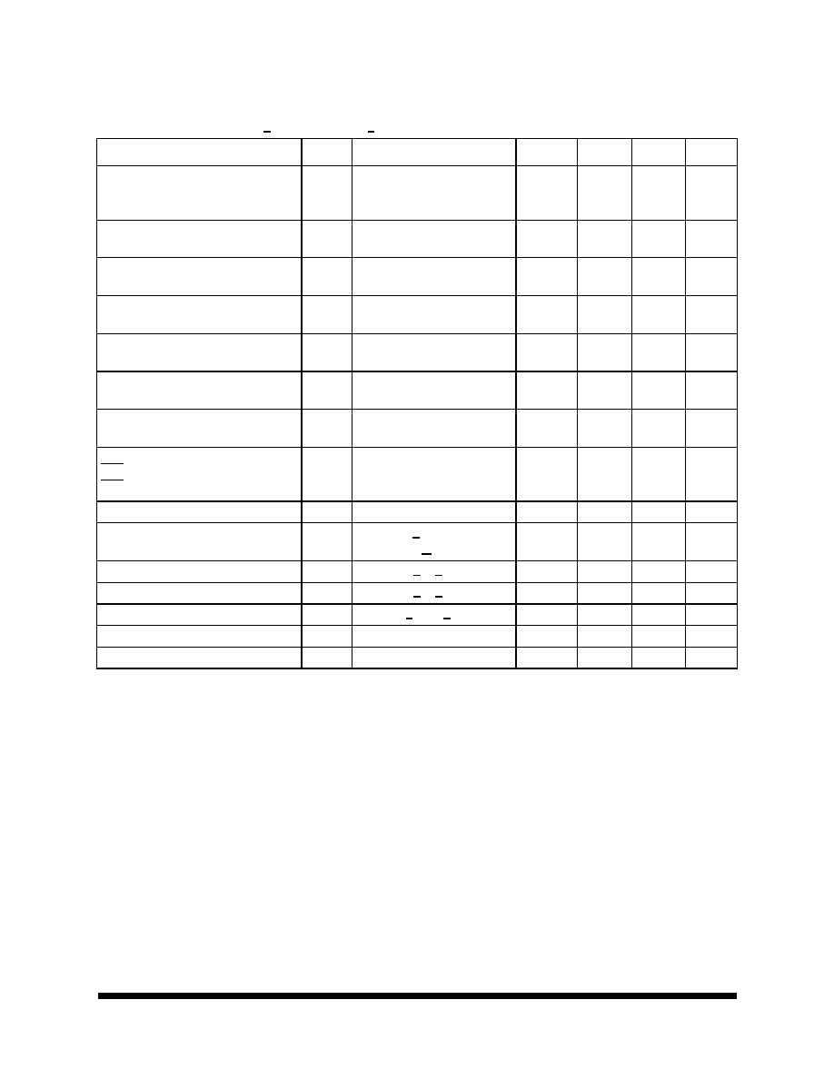
4. DC E
LECTRICAL
C
HARACTERISTICS
(V
CC
= 3.3V + 0.3V, V
CC
Q = 3.3V + 0.3V, T
A
= -55
TO
125∞C,
UNLESS
OTHERWISE
SPECIFIED
)
P
ARAMETER
S
YMBOL
T
EST
C
ONDITIONS
S
UBGROUPS
M
IN
M
AX
U
NITS
Operating Current
1,2,3
I
CC1
Burst length
= 1
t
RC
= min
CAS Latency = 2
1, 2, 3
460
mA
CAS Latency = 3
460
Standby Current in Power Down
4
I
CC2P
CKE = V
IL
t
CK
= 12 ns
1, 2, 3
12
mA
CC
P
ARAMETER
S
YMBOL
M
IN
M
AX
U
NIT
Supply Voltage
V
CC
, V
CCQ
1,2
3.0
3.6
V
V
SS
, V
SSQ
3
0
0
V
Input High Voltage
V
IH
1,4
2.0
V
CC
+ 0.3
V
Input Low Voltage
V
IL1,5
-0.3
.8
V
1. All voltage referred to VSS
2. The supply voltage with all
V
CC
and V
CCQ
pins must be on the same level
3. The supply voltage with all V
SS
and V
SSQ
pins must be on the same level
4.
V
IH
(max) =
V
CC
+2.0V for pulse width
<3ns at V
CC
5.
V
IL
(min) =
V
SS
-2.0V for pulse width
<3ns at V
SS
72SD3232
M
e
m
o
r
y
4
All data sheets are subject to change without notice
©2004 Maxwell Technologies
All rights reserved.
1 Gbit(32-Meg X 32-Bit X 4-Banks) SDRAM
03.25.04Rev 1
Standby Current in Power Down
( input signal stable)
5
I
CC2PS
CKE = V
IL
t
CK
= 0
1, 2, 3
8
mA
Standby Current in non power down
6
I
CC2N
CKE, CS = V
IH
t
CK
= 12 ns
1, 2, 3
80
mA
Standby Current in non power down
( Input signal stable)
7
I
CC2NS
CKE = V
IH
t
CK
= 0
1, 2, 3
36
mA
Active standby current in
power down
1,2,4
I
CC3P
CKE = V
IL
t
CK
= 12 ns
1, 2, 3
16
mA
Active standby current in power down
(input signal stable)
2,5
I
CC3PS
CKE = V
IL
t
CK
= 0
1, 2, 3
12
mA
Active standby power in non power
down
1,2,6
I
CC3N
CKE, CS = V
IN
t
CK
= 12 ns
1, 2, 3
120
mA
Active standby current in non power
down ( input signal stable)
2,7
I
CC3NS
CKE = V
IH
t
CK
= 0
1, 2, 3
60
mA
Burst Operating Current
1,2,8
CAS Latency = 2
CAS Latency = 3
I
CC4
t
CK
= min
BL = 4
1, 2, 3
440
580
mA
Refresh Current
3
I
CC5
t
RC
= min
1, 2, 3
880
mA
Self Refresh current
9
I
CC6
V
IH
>V
CC
- 0.2V
V
IL
< 0.2 V
1, 2, 3
12
mA
Input Leakage Current - CLK 1 & 2
I
LI
0<V
IN
<V
CC
1, 2, 3
-2
4
uA
Input Leakage Current - All Other
I
LI
0<V
IN
<V
CC
1, 2, 3
-4
4
uA
Output Leakage Current
I
LO
0<VOUT<V
CC
1, 2, 3
-1.5
1.5
uA
Output high voltage
V
OH
I
OH
= -4mA
1, 2, 3
2.4
V
Output low voltage
V
OL
I
OL
= 4 mA
1, 2, 3
0.4
V
1. ICC1 depends on output load conditions when the device is selected. ICC(max) is specified with the output open.
2. One Bank operation.
3. Input signals are changed once per one clock.
4. After power down mode, CLK operating current.
5. Afer power down mode, no CLK operating current.
6. Input signals are changed once per two clocks.
7. Input signals are VIH or VIL fixed.
8. Input signals are changed once per four clocks.
9. After self refresh mode set, self refresh current. Use self reset only at temperatures below 70∞C
T
ABLE
4. DC E
LECTRICAL
C
HARACTERISTICS
(V
CC
= 3.3V + 0.3V, V
CC
Q = 3.3V + 0.3V, T
A
= -55
TO
125∞C,
UNLESS
OTHERWISE
SPECIFIED
)
P
ARAMETER
S
YMBOL
T
EST
C
ONDITIONS
S
UBGROUPS
M
IN
M
AX
U
NITS

72SD3232
M
e
m
o
r
y
5
All data sheets are subject to change without notice
©2004 Maxwell Technologies
All rights reserved.
1 Gbit(32-Meg X 32-Bit X 4-Banks) SDRAM
03.25.04Rev 1
T
ABLE
5. AC Electrical Characteristics
(V
DD
=3.3V + 0.3V, V
DD
Q = 3.3V + 0.3V, T
A
= -55
TO
125∞C,
UNLESS
OTHERWISE
SPECIFIED
)
P
ARAMETER
S
YMBOL
S
UBGROUPS
M
IN
T
YP
M
AX
U
NIT
System clock cycle time
1
(CAS latency = 2)
(CAS latency = 3)
t
CK
9, 10, 11
10
7.5
ns
CLK high pulse width
1,7
t
CKH
9, 10, 11
2.5
ns
CLK low pulse width
1,7
t
CKL
9, 10, 11
2.5
ns
Access time from CLK
1,2
(CAS latency = 2)
(CAS latency = 3)
t
AC
9, 10, 11
6
6
ns
Data-out hold time
1,2
t
OH
9, 10, 11
2.7
ns
CLK to Data-out low impedance
1,2,3,7
t
LZ
9, 10, 11
2
ns
CLK to Data-out high impedance
1,4,7
(CAS latency = 2, 3)
t
HZ
9, 10, 11
5.4
ns
Input setup time
1,5,6
t
AS
, t
CS,
t
DS
, t
CES
9, 10, 11
1.5
ns
CKE setup time for power down exit
1
t
CESP
9, 10, 11
1.5
ns
Input hold time
1,6
t
AH
, t
CH
, t
DH
t
CEH
9, 10, 11
1.5
ns
Ref/Active to Ref/Active command period
1
t
RC
9, 10, 11
70
ns
Active to Precharge command period
1
t
RAS
9, 10, 11
50
120000
ns
Active command to column command
(same bank)
1
t
RCD
9, 10, 11
20
ns
Precharge to Active command period
1
t
RP
9, 10, 11
20
ns
Write recovery or data-in to precharge
lead time
1
t
DPL
9, 10, 11
20
ns
Active( a) to Active (b) command period
t
RRD
9, 10, 11
20
ns
Transition time(rise and fall)
7
t
T
9, 10, 11
1
5
ns
Refresh Period
t
REF
9, 10, 11
16
6.4
ms
105∞C
32
16
8
85∞C
64
70∞C
128
1. AC measurement assumes t
T
=1ns. Reference level for timing of input signals is 1.5V
2. Access time is measured at 1.5V.
3. t
LZ
(min) defines the time at which the outputs achieve the low impedance state.
4. t
HZ
(min) defines the time at which the outputs achieve the high impedance state.
5. tCES defines CKE setup time to CLK rising edge except for the power down exit command.
6. t
AS
/t
AH
: Address, tC/tCH: /CS, /RAS, /CAS, /WE, DQM
7. Guarenteed by design. (Not Tested)
8. Guarenteed by Device Characterization. ( Not 100% Tested)