
CP1117
Low Dropout Linear Regulator
* All specs and applications shown above subject to change without prior notice.
1F-5 NO.66 SEC.2 NAN-KAN RD ., LUCHU , TAOYUAN, TAIWAN
Email: server@ceramate.com.tw
Tel:886-3-3214525 Http: www.ceramate.com.tw
Fax:886-3-3521052
Page
1 of 12
Rev 1.4 Apr.29, 2005
General Description Features
The CP1117 is a series of low dropout three-terminal Low dropout voltage: 1.2V at 1A output current
regulators with a dropout of 1.2V at 1A output current. Trimmed current limit
The CP1117 has an adjustable version, that can On-chip thermal shutdown
provide the output voltage from 1.25V to 12V with only 2 Three-terminal adjustable of fixed 1.5V, 1.8V,
external resistors. 2.5V, 3.3V, 5V
The CP1117 series provides current limiting and
thermal shutdown. Its circuit includes a trimmed bandgap
reference to assure output voltage accuracy to be
within 1%. Current limit is trimmed to ensure specified
Applications
output current and controlled short-circuit current.
Onchip thermal shutdown provides protection against any PC Motherboard
combination of overload and ambient temperature that LCD Monitor
would create excessive junction temperature. Graphic Card
The CP1117 eries is available in the industry DVD-Video Player
standard SOT-223 power package NIC/Switch
Telecom Equipment
ADSL Modem
Printer and other Peripheral Equipment
SOT-223
SOT-223
Pin Configurations
INPUT
OUTPUT
ADJ/GND
V
OUT
1
2
3
Operation junction temp.: 0 to 125
TO-252
TO-252
INPUT
OUTPUT
ADJ/GND
V
OUT
1
2
3
CP1117
Low Dropout Linear Regulator
* All specs and applications shown above subject to change without prior notice.
1F-5 NO.66 SEC.2 NAN-KAN RD ., LUCHU , TAOYUAN, TAIWAN
Email: server@ceramate.com.tw
Tel:886-3-3214525 Http: www.ceramate.com.tw
Fax:886-3-3521052
Page
2 of 12
Rev 1.4 Apr.29, 2005
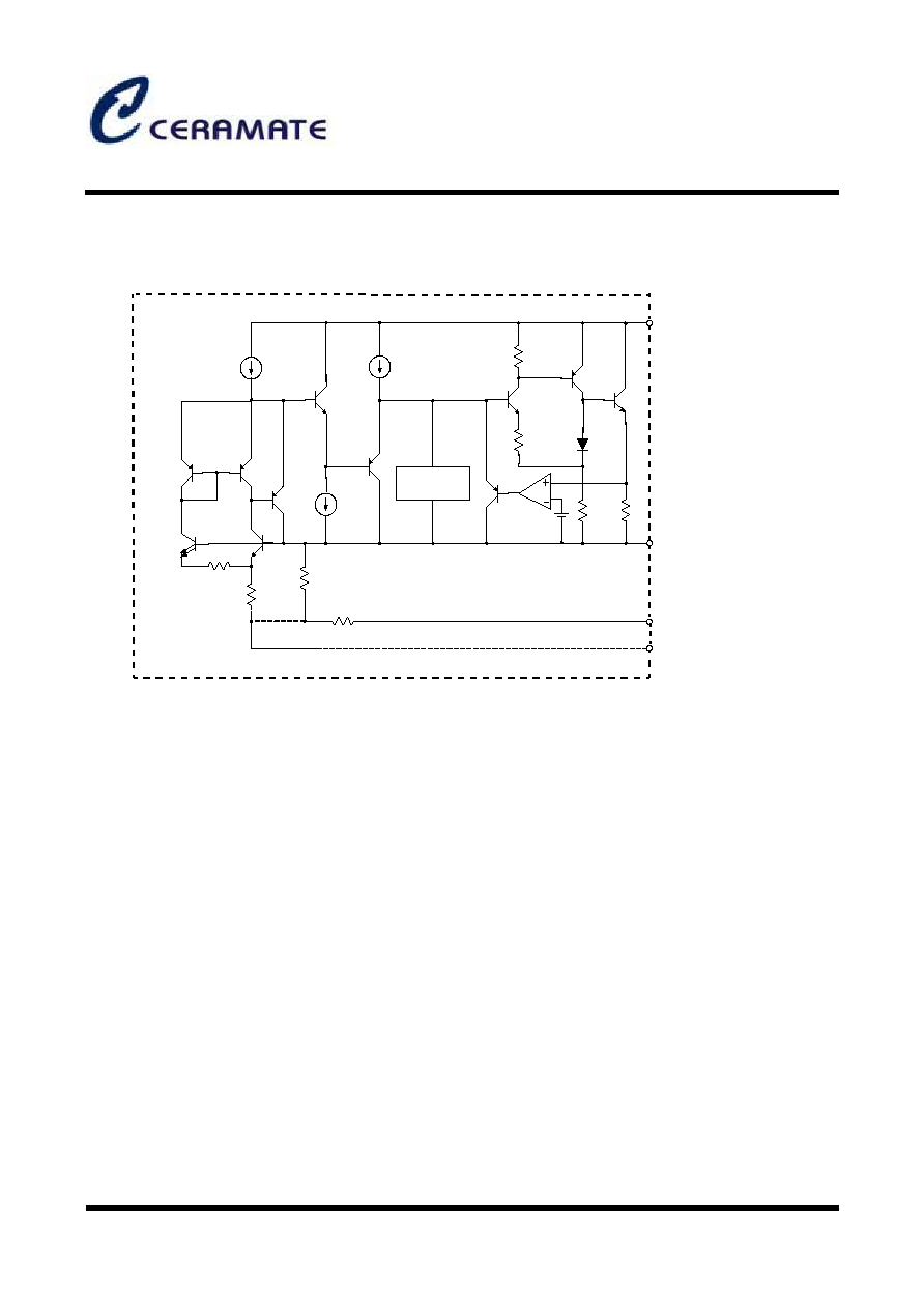
Functional Block Diagram
GND (Fixed Output)
ADJ (Adjustable Output)
Thermal
Shutdown
Out
+
-
INPUT
OUTPUT
Figure
1
. Functional Block Diagram of
CP
1117

CP1117
Low Dropout Linear Regulator
* All specs and applications shown above subject to change without prior notice.
1F-5 NO.66 SEC.2 NAN-KAN RD ., LUCHU , TAOYUAN, TAIWAN
Email: server@ceramate.com.tw
Tel:886-3-3214525 Http: www.ceramate.com.tw
Fax:886-3-3521052
Page
3 of 12
Rev 1.4 Apr.29, 2005
Order Information
Package
Temperature
Range
Part Number Packing Type Marking
CP1117 ADJ-A Tape/Reel CP1117 ADJ-A
CP1117 1.5-A Tape/Reel CP1117 1.5-A
CP1117 1.8-A Tape/Reel CP1117 1.8-A
CP1117 2.5-A Tape/Reel CP1117 2.5-A
CP1117 3.3-A Tape/Reel CP1117 3.3-A
TO-252
CP1117 5.0-A Tape/Reel CP1117 5.0-A
CP1117 ADJ-B Tape/Reel ADJ-B
CP1117 1.5-B Tape/Reel 1.5-B
CP1117 1.8-B Tape/Reel 1.8-B
CP1117 2.5-B Tape/Reel 2.5-B
CP1117 3.3-B Tape/Reel 3.3-B
SOT-223
0 ~125
CP1117 5.0-B Tape/Reel 5.0-B
CP 1117 XXX X X
T: Tube
R: Reel
A: TO-252
B: SOT-223
ADJ
1.5V
1.8V
2.5V
3.3V
5.0V

CP1117
Low Dropout Linear Regulator
* All specs and applications shown above subject to change without prior notice.
1F-5 NO.66 SEC.2 NAN-KAN RD ., LUCHU , TAOYUAN, TAIWAN
Email: server@ceramate.com.tw
Tel:886-3-3214525 Http: www.ceramate.com.tw
Fax:886-3-3521052
Page
4 of 12
Rev 1.4 Apr.29, 2005
Recommended Operating Conditions
Parameter Value Unit
V
IN
20 V
Maximum Junction Temperature 150
o
C
Storage Temperature Range -65 ~ 150
o
C
Lead Temperature (Soldering, 10 sec.) 300
o
C
ESD (Machine Model) 600 V
Parameter Min Max
Unit
V
IN
15
V
Operating Junction Temperature Range 0 125
o
C
Absolute Maximum Ratings (Note 1)
Note 1: Stresses greater than those listed under "Absolute Maximum Ratings " may cause permanent damage to the
device. These are stress ratings only, and functional operation of the device at these or any other conditions beyond
those indicated under "Recommended Operating Conditions" is not implied. Exposure to "Absolute Maximum
Ratings " for extended periods may affect device reliability.
CP1117
Low Dropout Linear Regulator
* All specs and applications shown above subject to change without prior notice.
1F-5 NO.66 SEC.2 NAN-KAN RD ., LUCHU , TAOYUAN, TAIWAN
Email: server@ceramate.com.tw
Tel:886-3-3214525 Http: www.ceramate.com.tw
Fax:886-3-3521052
Page
5 of 12
Rev 1.4 Apr.29, 2005
Electrical Characteristics
Operating Conditions: V
IN
1
0V,
T
J
=25
o
C unless otherwise specified.
Paramete r Conditions Min Ty p. Max Unit
Reference Voltage
CP1117- ADJ IOUT = 10m, VIN-VOUT = 2V
10mAIOUT1A, 1.4VVIN-VOUT8V,
PMaximum Power Dissipation
1.238
1.225
1.250
1.250
1.264
1.270
V
CP1117-1.5, IOUT = 10m, VIN = 3.5V
10mAIOUT1A, 3.0VVIN10V
1.485
1.470
1.5
1.5
1.515
1.530
V
CP1117-1.8, IOUT = 10m, VIN = 3.8V
10mAIOUT1A, 3.2VVIN10V
1.782
1.746
1.8
1.8
1.818
1.854
V
CP1117-2.5, IOUT = 10m, VIN = 4.5V
10mAIOUT1A, 3.9VVIN10V
2.475
2.450
2.5
2.5
2.525
2.550
V
CP1117-3.3, IOUT = 10m, VIN = 5.0V
10mAIOUT1A, 4.75VVIN10V
3.267
3.235
3.3
3.3
3.333
3.365
V
Output Voltage
CP1117-5.0, IOUT = 10m, VIN = 7.0V
10mAIOUT1A, 6.5VVIN12V
4.950
4.900
5.0
5.0
5.050
5.100
V
CP1117-ADJ
IOUT = 10Ma, 1.5VVIN-VOUT10V
0.035 0.2
CP1117-1.5
IOUT = 10mA, 1.5VVIN-VOUT10V
1 6 mV
CP1117-1.8
IOUT = 10mA, 1.5VVIN-VOUT10V
1 6 mV
CP1117-2.5
IOUT = 10mA, 1.5VVIN-VOUT10V
1 6 mV
CP1117-3.3
IOUT = 10mA, 1.5VVIN-VOUT10V
1 6 mV
Line Regulation
CP1117-5.0
IOUT = 10mA, 1.5VVIN-VOUT10V
1 10
mV
CP1117-ADJ
VIN -VOUT = 2V, 10mAIOUT1
0.2 0.4
CP1117-1.5
VIN -VOUT = 2V, 10mAIOUT1
1 10
mV
CP1117-1.8
VIN -VOUT = 2V, 10mAIOUT1
1
10
mV
CP1117-2.5
VIN -VOUT = 2V, 10mAIOUT1
1
10
mV
CP1117-3.3
VIN -VOUT = 2V, 10mAIOUT1
1
10
mV
Load Regulation
CP1117-5.0
VIN -VOUT = 2V, 10mAIOUT1
1
10
mV