 | –≠–ª–µ–∫—Ç—Ä–æ–Ω–Ω—ã–π –∫–æ–º–ø–æ–Ω–µ–Ω—Ç: CP3800N | –°–∫–∞—á–∞—Ç—å:  PDF PDF  ZIP ZIP |
Features
∑ Wide supply voltage operating range: 1.8 to13 V
∑ Low current consumption: Typically 5.5 mA
in operation, 1
µA or less in stand-by
∑ High speed operation is possible: Maximum
1 MHz
∑ The error amplifier gain is set inside the IC,
so peripheral components are minimized.
∑ Incorporates a soft start circuit.
∑ Incorporates a timer-latch type short circuit
detection circuit (SCP).
∑ Totem-pole type output with adjustable on/off
current (for NPN transistors)
∑ Incorporates a stand-by function.
Applications
∑ Power source for battery-powered equipment
∑ Power source for cameras, camcorders, VCRs,
PDAs, electronic data banks, and hand-held
Communication equipment
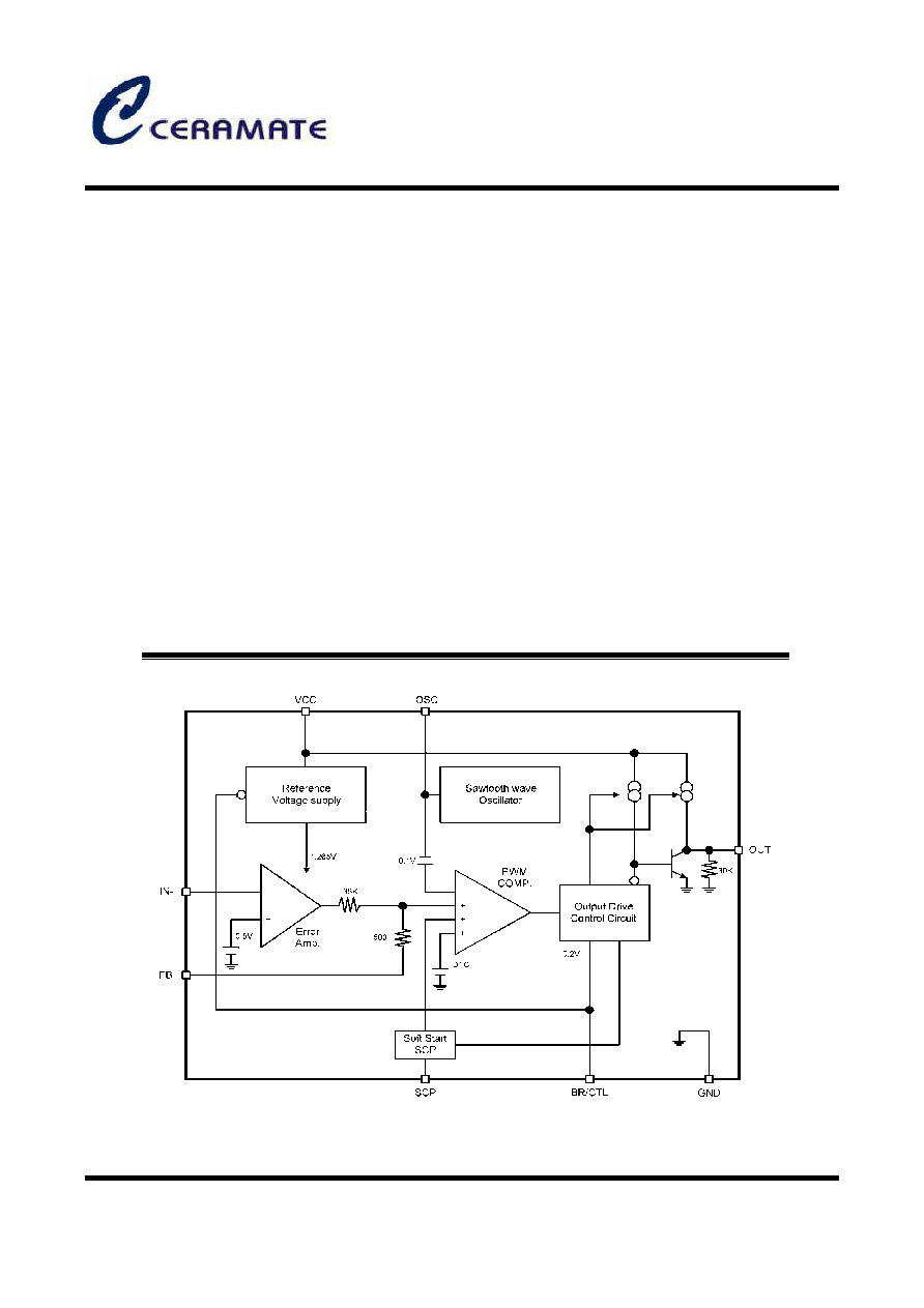
General Description
The
CP3800 is a single-channel switching
regulator control IC for low voltage applications
incorporating a soft start function and short circuit
detection function. The device has a low minimum
operating voltage of 1.8 V and is ideal for the
power supply of battery-operated electronic
equipment.
The CP
3800 can be operated on two types: non-
insulated input/output choppers (step-up, step-
down , and insulated input/output converters (fly-
back). The former type is used for DC/DC
converters and the latter type is used for DC/DC
converts and line-operation-type power supplies.
Block Diagram
CP3800
Switching Regulator Power Controller
* All specs and applications shown above subject to change without prior notice.
1F-5 NO.66 SEC.2 NAN-KAN RD ., LUCHU , TAOYUAN, TAIWAN
Email: server@ceramate.com.tw
Tel:886-3-3214525
Http: www.ceramate.com.tw
Fax:886-3-3521052
Page 1 of 19
Rev 1.0 Mar.31,2003

Pin Configuration
Pin Description
Pin No.
Symbol
I/O
Description
1
IN-
I
Error amplifier inverting input pin
2
SCP
--
Soft start and SCP setting capacitor connection pin
3
VCC
--
Power supply pin
4
BR/CTL
I
Output current setting and control pin
5
OUT
O
Totem-pole type output pin
6
GND
--
Ground pin
7
OSC
--
Capacitor and resistor connection pin for setting the oscillation
frequency
8
FB
O
Error amplifier output pin
* All specs and applications shown above subject to change without prior notice.
1F-5 NO.66 SEC.2 NAN-KAN RD ., LUCHU , TAOYUAN, TAIWAN
Email: server@ceramate.com.tw
Tel:886-3-3214525
Http: www.ceramate.com.tw
Fax:886-3-3521052
Page
2 of 19
Rev 1.0 Mar.31,2003
CP3800
Switching Regulator Power Controller
Ordering Information
CP3800 X X
Package Packing
N: DIP-8 BLANK: TUBE
S: SOP-8
A: TAPING
T: TSSOP-8

Absolute Maximum Ratings
(T
a
=+25
0
C)
Rated Value
Parameter
Symbol
Condition
Min.
Max.
Unit
Power supply voltage
V
CC
--
--
3
V
Output source current
I
O
+
--
--
-50
mA
Output sink current
I
O
-
--
--
50
mA
P
D
SOP-8, Ta +25∞C
--
570
mW
Allowable dissipation
P
D
TSSOP-8, Ta +25∞C
--
430
mW
Operating temperature
T
OP
--
-30
+85
0
C
Storage temperature
T
stg
--
-55
+125
0
C
ESD Classification
MIL-STD-883
Class 2
*
: When mounted on a 10 cm square double-sided epoxy board
WARNING: Semiconductor devices can be permanently damaged by application of stress (voltage,
current, temperature, etc.) in excess of absolute maximum ratings. Do not exceed these ratings.
Recommended Operating Conditions
(Ta=+25
0
C)
Values
Parameter
Symbol
Min.
Typ.
Max.
Unit
Power supply voltage
V
CC
1.8
--
12.0
Error amplifier input voltage
V
I
-0.2
--
1.0
BR/CTL pin input voltage
V
BR
-0.2
--
V
CC
Output source current
I
O
+
-20
--
--
Output sink current
I
O
-
--
--
40
SCP pin capacitance
C
PE
--
0.1
--
Phase compensation capacitance
C
P
--
0.1
--
Output current setting resistance
R
B
150
390
5000
Timing resistance
R
T
1.0
3.0
10.0
Timing capacitance
C
T
100
270
10000
pF
Oscillation frequency
f
OSC
10
500
1000
kHz
Operating temperature
T
OP
-30
+25
+85
∞C
WARNING: Recommended operating conditions are normal operating ranges for the semiconductor
device. All the device's electrical characteristics are warranted when operated within these ranges.
Always use semiconductor devices within the recommended operating conditions. Operation outside
these ranges may adversely affect reliability and could result in device failure.
CP3800
Switching Regulator Power Controller
* All specs and applications shown above subject to change without prior notice.
1F-5 NO.66 SEC.2 NAN-KAN RD ., LUCHU , TAOYUAN, TAIWAN
Email: server@ceramate.com.tw
Tel:886-3-3214525
Http: www.ceramate.com.tw
Fax:886-3-3521052
Page
3 of 19
Rev 1.0 Mar.31,2003

Electrical Characteristics
(V
CC
=+2V, Ta=+25
0
C)
Values
Parameter
Symbol
Condition
Min. Typ. Max.
Unit
Reset voltage
V
R
--
--
0.9
V
Circuit to prevent
malfunction at low
input voltage
(U.V.L.O.)
Threshold voltage
V
TH
--
1.1
1.3
1.5
V
Charging current
I
CS
V
SCP
=0V
-1.5
-1.0
-0.7 A
Soft start
Voltage at soft start
completion
V
ts
--
0.7
0.8
0.9
V
Charging current
I
CPC
V
SCP
=0V
-1.5
-1.0
-0.7 A
Short circuit
detection (S.C.P.)
Threshold voltage
V
tPC
--
0.7
0.8
0.9
V
Oscillation frequency
f
OSC
R
T
=3.3k, C
T
=270pF
400
500
600
kHz
Frequency input
Stability
f
dV
V
CC
=2V to 12V
--
2
10
%
Sawtooth wave
oscillator (OSC)
Frequency variation
with temperature
f
dT
Ta =-30
0
C to 85
0
C
--
5
--
%
Input threshold
Voltage
V
T
V
FB
= 450mV
480
500
520
mV
V
T
input stability
V
TdV
V
CC
=2V to 12V
--
5
20
mV
V
T
variation with
Temperature
V
TdT
Ta = -30
0
C to 85
0
C
--
1
--
%
Input bias current
I
B
V
IN
= 0V
-1.0
-0.2
1.0
A
Voltage gain
A
V
--
70
100
145 V/V
Frequency bandwidth
BW
A
V
= 0 dB
--
6
--
MHz
V
OM
+
0.78 0.87
--
V
Maximum output
voltage range
V
OM
_
--
--
0.05
0.2
V
Output source current
I
OM
+
--
-40
-24
A
Error amplifier
Output sink current
I
OM
_
V
FB
= 450mV
24
40
--
A
Idle period
adjustment section
Maximum duty cycle
T
DUTY
R
T
=3.3k, C
T
=270pF
f
OSC
= 500KHz
75
--
85
%
V
OH1
R
B
= 390, I
O
= -15 mA 1.0
1.2
--
V
V
OH2
R
B
= 750, V
CC
= 1.8V
I
O
= -10 mA
0.8
1.0
--
V
V
OL1
R
B
= 390, I
O
= -15 mA
--
0.1
0.2
V
Output voltage
V
OL2
R
B
= 750, V
CC
= 1.8V
I
O
= -10 mA
--
0.1
0.2
V
Output source current
I
O
+
R
B
= 390, V
O
= 0.9V
--
-30
-20
mA
Output sink current
I
O
-
R
B
= 390, V
O
= 0.3V
30
60
--
mA
Output section
Pull down resistance
R
O
--
20
30
40
CP3800
Switching Regulator Power Controller
* All specs and applications shown above subject to change without prior notice.
1F-5 NO.66 SEC.2 NAN-KAN RD ., LUCHU , TAOYUAN, TAIWAN
Email: server@ceramate.com.tw
Tel:886-3-3214525
Http: www.ceramate.com.tw
Fax:886-3-3521052
Page
4 of 19
Rev 1.0 Mar.31,2003

Pin voltage
V
BR
R
B
= 390
0.10 0.19 0.25
V
Input off condition
I
OFF
-20
--
0
A
Input on condition
I
ON
--
--
-45
A
Output current
Setting section/
Control section
Pin current range
I
BR
--
-1.8
--
-0.1
Stand-by current
I
CCS
BR/CTL pin open or
V
CC
--
--
1
A
Entire device
Average supply current
I
CC
R
B
= 390,V
CC
=2~12V
--
5.5
10.0
Timing Chart
CP3800
Switching Regulator Power Controller
* All specs and applications shown above subject to change without prior notice.
1F-5 NO.66 SEC.2 NAN-KAN RD ., LUCHU , TAOYUAN, TAIWAN
Email: server@ceramate.com.tw
Tel:886-3-3214525
Http: www.ceramate.com.tw
Fax:886-3-3521052
Page
5 of 19
Rev 1.0 Mar.31,2003
t
S
t
PE
ON
OFF
FB pin voltage
Reference input for short circuit
detection comparator
Idle period setting voltage
Sawtooth wave output
Soft start setting voltage
OUT pin waveforms
SCP pin waveforms
Power supply control SW
Soft start
Output
short
circuit
Output short circuit
Short circuit
detection