 | –≠–ª–µ–∫—Ç—Ä–æ–Ω–Ω—ã–π –∫–æ–º–ø–æ–Ω–µ–Ω—Ç: CTM8B57E | –°–∫–∞—á–∞—Ç—å:  PDF PDF  ZIP ZIP |

FEATURES
GENERAL DESCRIPTION
BLOCK DIAGRAM
CTM8B5X series is an EPROM based 8-bit micro-
controller which employs a full CMOS technology
enhanced with low-cost, high speed and high noise
immunity. Watchdog Timer, RAM, EPROM, tri-state
I/O port, power down mode, and real time program-
mable clock/counter are integrated into this chip.
CTM8B5X contains 33 instructions, all are single
cycle except for program branches which take two
cycles.
On chip memory is available with 512x14 bits of
EPROM for CTM8B54E/55E, 1Kx14 bits of EPROM
for CTM8B56E, 2Kx14 bits of EPROM for
CTM8B57E and 24 to 72 bytes of static RAM.
∑ Total of 33 single word instructions .
∑ The fast execution time may be 200ns for all single
cycle instructions under 20MHz operating.
∑ Operating voltage range: 2.3V ~ 6.5V
∑ 8-bit data bus.
∑ 14-bit instruction word.
∑ Four-level stacks.
∑ On chip EPROM size : 512x14 bits for CTM8B54E/55E,
1Kx14 bits for CTM8B56E,
2Kx14 bits for CTM8B57E.
∑ Internal RAM size : 25 bytes for CTM8B54E/56E,
24 bytes for CTM8B55E,
∑ 72 bytes for CTM8B57E.
∑ Direct and indirect addressing modes for data accessing
∑ 8-bit real time clock/counter with 8-bit programmable
prescaler.
∑ Internal power-on Reset.
∑ Device Reset Timer.
∑ Code protection.
∑ Sleep mode for power saving.
∑ On chip Watchdog Timer(WDT) based on internal RC
oscillator.
∑ Three I/O ports PA, PB nad PC with independent direc-
tion control.
Four-level
Stack
RAM
Configuration
Word
OSCO
OSCI
MCLR
WDT/Timer0
Prescaler
Oscillator
Circuit
Osc Mode
Select
Sleep
WatchDog
Timer
E
n
a
b
l
e
/
D
i
s
a
b
l
e
T0CKI
Timer0
WDT
Time Out
T0MODE
Register
6
V
dd
V
ss
Program
Counter
EPROM
Instruction
Register
Instruction
Decoder
FSR
PortA
PortB
Status
6
Accumulator
ALU
11
11
14
14
8
8
D
a
t
a
8
4
PA3:PA0
PB7:PB0
2
PortC
8
PC7:PC0
24, 25 or 27 Bytes
512 X 14 TO
2048 X 14
Only in CTM8B55E/57E
∑ 4 types of oscillator can be selected by code options:
- RC : Low-cost RC oscillator
- XTAL : Standard crystal oscillator
- HFXTAL : High frequency crystal oscillator
- LFXTAL : Low frequency crystal oscillator
CMOS Microcontroller
EPROM-Based 8-Bit
CTM8B54E/55E/56E/57E
* All specs and applications shown above subject to change without prior notice.
1F-5 NO.66 SEC.2 NAN-KAN RD ., LUCHU , TAOYUAN, TAIWAN, R.O.C
Email: server@ceramate.com.tw
Tel:886-3-3529445
Http: www.ceramate.com.tw
Fax:886-3-3521052
Page 1 of
23
Rev 1.1 Dec 26,2001
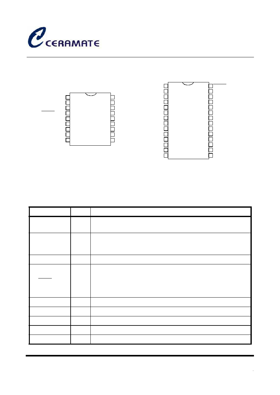
1.0 PIN CONNECTION
2.0 PIN DESCRIPTIONS
PA2
PA3
PA1
PA0
OSCO
OSCI
Vdd
Vss
T0CKI
MCLR/Vpp
PB0
PB1
PB2
PB3
PB7
PB6
PB5
PB4
1
2
3
4
8
5
7
9
6
18
17
16
15
11
14
12
10
13
CTM8B54E
PA2
PA3
PA1
PA0
OSCO
OSCI
Vdd
Vss
T0CKI
MCLR/Vpp
PB0
PB1
PB2
PB3
PB7
PB6
PB5
PB4
1
2
3
4
8
5
7
9
6
18
17
16
15
11
14
12
10
13
CTM8B55E
N/C
N/C
19
20
21
22
23
24
25
26
27
28
PC0
PC1
PC2
PC3
PC4
PC5
PC6
PC7
CTM8B57E
CTM8B56E
Name
I/O
Descriptions
OSCI
I
RC type: Input pin of RC oscillator
XTAL type: Input terminal of crystal oscillator
OSCO
O
RC type: OSCO outputs with 1/4 frequency of OSCI to denotes the cycle
rate for instruction.
XTAL type: Output terminal of crystal oscillator
T0CKI/SCL
I
Input pin of real time counter/clock. Must be tied to Vss or Vdd if not in use.
MCLR/Vpp
I
Input pin for device reset or high voltage programming input for EPROM. If
this pin is low, the device is reset.
In programmimg mode, this pin is connected to 12V. In normal operating
mode, this pin must not exceed Vdd to avoid entering unintended program-
ming mode.
PA0~PA3
I/O
PA0~PA3 as bi-directional I/O port
PB0~PB7
I/O
PB0~PB7 as bi-directional I/O port
PC0~PC7
I/O
PC0~PC7 as bi-directional I/O port
Vdd
-
Power supply
Vss
-
Ground
CMOS Microcontroller
EPROM-Based 8-Bit
CTM8B54E/55E/56E/57E
* All specs and applications shown above subject to change without prior notice.
1F-5 NO.66 SEC.2 NAN-KAN RD ., LUCHU , TAOYUAN, TAIWAN, R.O.C
Email: server@ceramate.com.tw
Tel:886-3-3529445
Http: www.ceramate.com.tw
Fax:886-3-3521052
Page 2 of
23
Rev 1.1 Dec 26,2001

3.0 FUNCTIONAL DESCRIPTIONS
3.1 REGISTER MAP
The register map of CTM8B5X is depicted as below:.
The Register Map of CTM8B54E/56E
Address
Description
00h
Indirect Addressing Register
01h
Timer0
02h
PC
03h
STATUS
04h
FSR
05h
PORTA
06h
PORTB
07h-1Fh
General Purpose Register
The Register Map of CTM8B55E
Address
Description
00h
Indirect Addressing Register
01h
Timer0
02h
PC
03h
STATUS
04h
FSR
05h
PORTA
06h
PORTB
07h
PORTC
08h-1Fh
General Purpose Register
The Register Map of CTM8B57E
Address
Description
FSR<6:5>
Bank 0
00
Bank 1
01
Bank 2
10
Bank 3
11
00h
Indirect Address-
ing Register
Map back to address in Bank 0
01h
Timer0
02h
PC
03h
STATUS
04h
FSR
05h
PORTA
06h
PORTB
07h
PORTC
08h~0Fh
General Purpose
Register
10h~1Fh
General Purpose
Register
30h~3Fh
General Purpose
Register
50h~5Fh
General Purpose
Register
70h~7Fh
General Purpose
Register
CMOS Microcontroller
EPROM-Based 8-Bit
CTM8B54E/55E/56E/57E
* All specs and applications shown above subject to change without prior notice.
1F-5 NO.66 SEC.2 NAN-KAN RD ., LUCHU , TAOYUAN, TAIWAN, R.O.C
Email: server@ceramate.com.tw
Tel:886-3-3529445
Http: www.ceramate.com.tw
Fax:886-3-3521052
Page 3 of
23
Rev 1.1 Dec 26,2001

3.1.1 INAR(Indirect Address Register) : R0
R0 is not a physically implemented register. It is used as an indirect addressing pointer. Any instruction
accessing this register can access data pointed by FSR(R4).
3.1.2 Timer0(8-bit real-time clock/timer) : R1
This register increases by an external signal edge applied to T0CKI pin, or by internal instruction cycle. It can
be read or written as any other register.
3.1.3 PC(Program Counter) : R2
This register increases itself every instruction cycle, except the following condition shown in Figure 1:
3.1.4 STATUS(Status Register): The content of R3 is listed in Table 1.
A10~A0
LCALL, LGOTO : from instruction word
RETIA : from STACK
Stack1
Stack2
Stack3
Stack4
LCALL
RETIA
FIGURE 1. Program Counter
TABLE 1. STATUS Register
Bit
Symbol
Description
0
C
Carry/borrow bit
ADDWF SUBWF
= 1, a carry occurred = 1, a borrow did not occur
= 0, a carry did not occur = 0, a borrow occurred
1
DC
Half carry/half borrow bit
ADDWF
= 1, a carry from the 4th low order bit of the result occurred
= 0, a carry from the 4th low order bit of the result did not occur
SUBWF
= 1, a borrow from the 4th low order bit of the result did not occur
= 0, a borrow from the 4th low order bit of the result occurred
2
Z
Zero bit:
= 1, the result of a logic operation is zero
= 0, the result of a logic operation is not zero
3
PD
Power down flag bit:
= 1, after power-up or by the CLRWDT instruction
= 0, by the SLEEP instruction
4
TO
Time overflow flag bit:
= 1, after power-up or by the CLRWDT or SLEEP instruction
= 0, a WDT time-overflow occurred
5, 6, 7
-
Unused
CMOS Microcontroller
EPROM-Based 8-Bit
CTM8B54E/55E/56E/57E
* All specs and applications shown above subject to change without prior notice.
1F-5 NO.66 SEC.2 NAN-KAN RD ., LUCHU , TAOYUAN, TAIWAN, R.O.C
Email: server@ceramate.com.tw
Tel:886-3-3529445
Http: www.ceramate.com.tw
Fax:886-3-3521052
Page 4 of
23
Rev 1.1 Dec 26,2001

3.1.5 FSR(File select register pointer): R4
Bit 0~4 are used to select up to 32 registers (address: 00h~1Fh) and Bit 5~6 are Bank Select (Bank0~3) in the
indirect addressing mode shown in Figure 2.
3.1.6 PORT A: R5
PA3:PA0, bi-directional I/O Register
3.1.7 PORT B: R6
PB7:PB0, bi-directional I/O Register
3.1.8 PORT C: R7
PB7:PB0, bi-directional I/O Register, and for MTU8B55E/57E only
3.1.9 T0MODE REGISTER: T0MODE is a write-only register and the content is listed in Table 2.
3.1.10 IOST (Control Port I/O Mode Register)
The IOST register is "write-only"
= 0, I/O pin in output mode;
= 1, I/O pin in input mode.
Bank 3
Bank 2
Bank 1
B7
B6
B5
B4
B3
B2
B1
B0
Indirect Addressing Mode
Location Select
Read 1
Bank Select
FIGURE 2. Data Memory Configuraion
00h
INAR
01h
Timer0
02h
PC
03h
STATUS
04h
FSR
05h
PORT A
06h
PORT B
07h
PORT C
08h
8 Bytes
SRAM
0Fh
Bank 0
SRAM
16 Bytes
10h
1Fh
30h
3Fh
50h
5Fh
70h
7Fh
Bank 0
CMOS Microcontroller
EPROM-Based 8-Bit
CTM8B54E/55E/56E/57E
* All specs and applications shown above subject to change without prior notice.
1F-5 NO.66 SEC.2 NAN-KAN RD ., LUCHU , TAOYUAN, TAIWAN, R.O.C
Email: server@ceramate.com.tw
Tel:886-3-3529445
Http: www.ceramate.com.tw
Fax:886-3-3521052
Page 5 of
23
Rev 1.1 Dec 26,2001