/home/web/doc/html/cet/168603
250
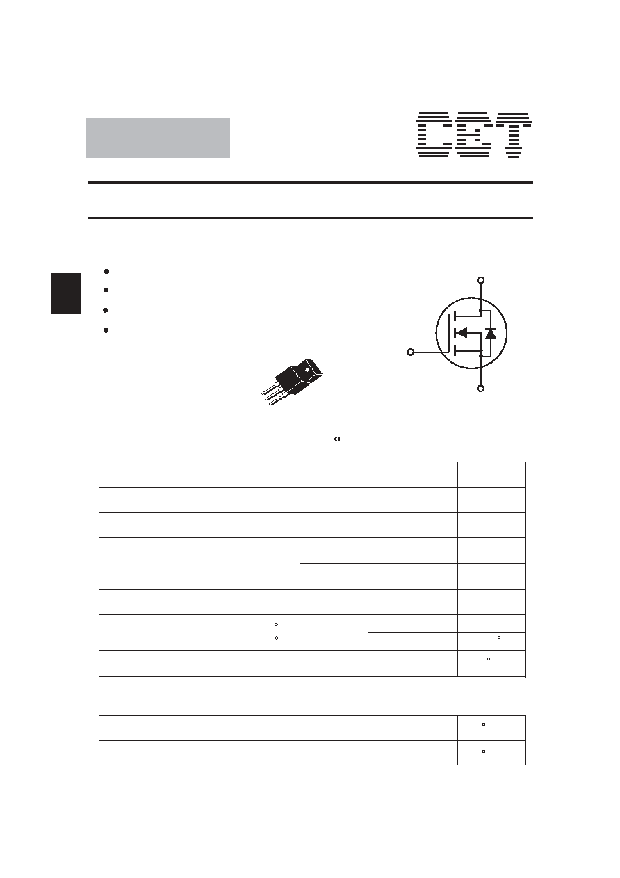
N-Channel Logic Level Enhancement Mode Field Effect Transistor
FEATURES
250V , 6A , R
DS(ON)
=450m @V
GS
=10V.
Super high dense cell design for extremely low R
DS(ON)
.
High power and current handling capability.
TO-220F full-pak for through hole
ABSOLUTE MAXIMUM RATINGS (Tc=25 C unless otherwise noted)
Parameter
Symbol
Limit
Unit
Drain-Source Voltage
V
DS
V
Gate-Source Voltage
V
GS
30
V
-Pulsed
I
D
6
A
I
DM
A
Drain-Source Diode Forward Current
I
S
6
A
Maximum Power Dissipation
P
D
W
Operating and Storage Temperautre Range
T
J
, T
STG
-50 to 150
C
THERMAL CHARACTERISTICS
Thermal Resistance, Junction-to-Case
Thermal Resistance, Junction-to-Ambient
R
JC
R
JA
3.3
65
/W
C
/W
C
@Tc=25 C
Derate above 25 C
0.3
W/ C
Drain Current-Continuous
S
G
D
6-102
Nov. 2002
24
CEFF634
TO-220F
S
D
G
38
6
ELECTRICAL CHARACTERISTICS (T
C
=25 C unless otherwise noted)
Parameter
Symbol
Condition
Min Typ Max Unit
OFF CHARACTERISTICS
Drain-Source Breakdown Voltage
BV
DSS
V
GS
= 0V, I
D
= 250
�
A
250
V
Zero Gate Voltage Drain Current
I
DSS
V
DS
= 250V, V
GS
= 0V
25
�
A
Gate-Body Leakage
I
GSS
V
GS
= 30V, V
DS
= 0V
100
nA
ON CHARACTERISTICS
a
Gate Threshold Voltage
V
GS(th)
V
DS
= V
GS
, I
D
= 250
�
A
2
4
V
Drain-Source On-State Resistance
R
DS(ON)
V
GS
= 10V, I
D
= 5.1A
450
m
On-State Drain Current
I
D(ON)
V
GS
= 10V, V
DS
= 10V
10
4.4
A
S
Forward Transconductance
FS
g
V
DS
= 50V, I
D
= 5.1A
DYNAMIC CHARACTERISTICS
b
Input Capacitance
C
ISS
C
RSS
C
OSS
Output Capacitance
Reverse Transfer Capacitance
V
DS
=25V, V
GS
= 0V
f =1.0MH
Z
630
P
F
100
P
F
P
F
40
SWITCHING CHARACTERISTICS
b
Turn-On Delay Time
Rise Time
Turn-Off Delay Time
t
D(ON)
t
r
t
D(OFF)
t
f
V
DD
= 125V,
I
D
= 5.6A,
V
GS
= 10V,
R
GEN
= 12
19
ns
ns
ns
ns
11
46
10
Total Gate Charge
Gate-Source Charge
Gate-Drain Charge
Q
g
Q
gs
Q
gd
V
DS
=200V, I
D
= 5.6A,
V
GS
=10V
33
nC
nC
nC
5
11
Fall Time
6-103
26
30
90
30
40
CEFF634
6
Parameter
Symbol
Condition
Min Typ Max Unit
ELECTRICAL CHARACTERISTICS (T
C
=25 C unless otherwise noted)
DRAIN-SOURCE DIODE CHARACTERISTICS
Diode Forward Voltage
V
SD
V
GS
= 0V, Is =8.1A
0.9
1.5
V
a
Notes
b.Guaranteed by design, not subject to production testing.
a.Pulse Test:Pulse Width 300 s, Duty Cycle 2%.
Figure 1. Output Characteristics
Figure 2. Transfer Characteristics
Figure 3. Capacitance
V
DS
, Drain-to Source Voltage (V)
V
GS
, Gate-to-Source Voltage (V)
V
DS
, Drain-to-Source Voltage (V)
I
D
,
D
r
ain
Current(A)
C
,
Capacitance
(pF)
I
D
,
D
r
ain
Current
(A)
6-104
0.1
1
2
4
6
10
8
25 C
-55 C
150 C
1.V
DS
=40V
2.Pulse Test
Figure 4. On-Resistance Variation with
Temperature
T
J
, Junction Temperature( C)
On-Resistance(Ohms)
R
DS(ON)
,
R
DS(ON)
,
N
or
maliz
e
d
-100
-50
0
50
100
200
3.0
2.5
2.0
1.5
1.0
0.5
0.0
V
GS
=10V
I
D
=5.1A
150
Ciss
Coss
Crss
900
750
600
450
300
150
0
0
10
20
30
40
50
12
10
8
6
4
2
0
0
1
2
3
4
5
6
V
GS
=10,9,8,7V
V
GS
=5V
V
GS
=6V
V
GS
=4V
CEFF634
6
with Temperature
Figure 6. Breakdown Voltage Variation
Figure 5. Gate Threshold Variation
with Temperature
Vth,
Normalized
Gate-Source
Threshold
Voltage
g
FS
,
Transconductance
(S)
V
GS
,
Gate
t
o
Source
Voltage
(V)
BV
DSS
,
Normalized
Drain-Source
Breakdown
Voltage
Is,
Source-drain
c
urrent
(A)
Figure 7. Transconductance Variation
with Drain Current
I
DS
, Drain-Source Current (A)
Figure 9. Gate Charge
Qg, Total Gate Charge (nC)
Figure 10. Maximum Safe
Operating Area
V
DS
, Drain-Source Voltage (V)
Figure 8. Body Diode Forward Voltage
Variation with Source Current
V
SD
, Body Diode Forward Voltage (V)
Tj, Junction Temperature ( C)
Tj, Junction Temperature ( C)
I
D
,
D
rain
Current
(A)
6-105
-50 -25
0
25
50
75 100 125 150
1.15
1.10
1.05
1.00
0.95
0.90
0.85
I
D
=250 A
1.30
1.20
1.10
1.0
0.90
0.80
0.70
0.60
-50 -25
0
25
50
75
100 125 150
V
DS
=V
GS
I
D
=250 A
10
10
0
10
10
3
2
1
10
-1
10
0
10
1
T
C
=25 C
Single Pulse
Tj=150 C
10
0
s
R
DS
(ON
) L
im
it
DC
1ms
10
m
s
10
0m
s
5
4
6
0
1
2
3
0
2
4
6
8
V
DS
=50V
20
10
0.1
1
0.4
0.6
0.8
1.2
1.0
V
GS
=0V
8
6
4
2
0
10
0
7
14
21
28
V
DS
=200V
I
D
=5.6A
CEFF634
6
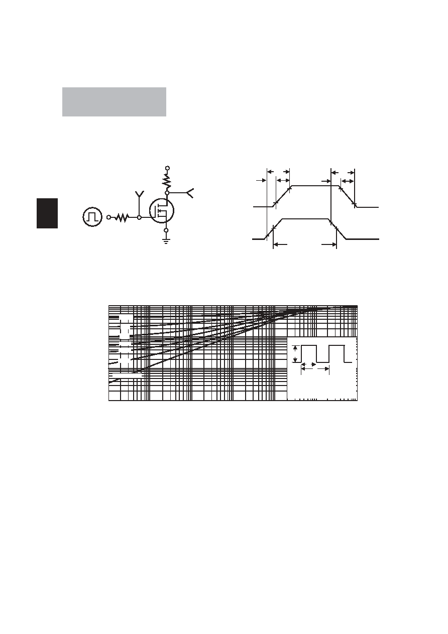
Figure 11. Switching Test Circuit
Figure 12. Switching Waveforms
t
V
V
t
t
d(on)
OUT
IN
on
r
10%
t
d(off)
90%
10%
10%
50%
50%
90%
t
off
t
f
90%
PULSE WIDTH
INVERTED
Transient
Thermal
Impedance
Square Wave Pulse Duration (sec)
Figure 13. Normalized Thermal Transient Impedance Curve
r(t),Normalized
Effective
V
DD
R
D
V
V
R
S
V
G
GS
IN
GEN
OUT
L
6-106
10
-5
10
-4
10
-3
10
-2
10
-1
P
DM
t
1
t
2
1. R
JC
(t)=r (t) * R
JC
2. R
JC
=See Datasheet
3. T
JM-
T
C
= P* R
JC
(t)
4. Duty Cycle, D=t1/t2
10
-3
10
-2
10
-1
10
0
10
1
10
0
Single Pulse
0.01
0.02
0.05
0.1
0.2
D=0.5
CEFF634
6