
CE
DB3/DC34/DB4/DB6
CHENYI ELECTRONICS
SILICON BIDIRECTIONAL DIAC
FEATURES
The three layer,two terminal, axial lead, hermetically sealed diacs are
designed specifically for triggering thyristors. They demonstrate low breakover
current at breakover voltage as they withstand peak pulse current,The breakover
symmetry is within three volts(DB3,DC34,DB4)or four volts(DB6).These diacs are
intended for use in thyrisitors phase control, circuits for lamp dimming,universal
motor speed control, and heat control.
JF's DB3/DC34/DB4/DB6 are bi-directional trigged diode designed to operate
in conjunction with Triacs and SCR's
ABSOLUTE RATINGS(LIMITING VALUES)
DB3 DC34
DB4
DB6
Power Dissipation on Printed
Circuit(L=10mm)
Repetitive Peak in-state tp=10u s
Current
F=100Hz
T
STG
/
T
J
Storage and Operating Junction Temperature
ELECTRCAL CHARACTERISTICS
DB3
DC34 DB4
DB6
c=22nF(Note 2)
Min
28
30
35
56
See diagram1
Typ
32
34
40
60
Max
36
38
45
70
|+VBO|-
c=22nF(Note 2)
|-VBO|
See diagram1
I=(
I
BO
to IF=10mA)
See diagram1
Vo
See diagram2
Min
V
IBO
c=22nF(Note 2)
Max
A
tr
See Diagram 3
Typ
S
V
B
=0.5
V
BO
max
see diagram 1
Notes: 1. Electrical characteristics applicable in both forward and reverse directions.
2. Connected in parallel with the devices.
Parameters
Symbols
Units
2.0
2.0
1.6
Value
Symbols
Parameters
-40 to +125/-40 to 110
mW
A
P
c
I
TRM
TA=50
150
2.0
VBO
Breakover Voltage(Note 2)
Output Voltage(Note 1)
Breakover Current(Note 1)
Max
| V|
IB
Leakage Current(Note 1)
Rise Time(Note 1)
Value
Dynamic Breakover
Voltage(Note 1)
Breakover Voltage Symmetry
Units
3
4
5
Test Conditions
Max
Min
10
10
V
V
V
A
5
100
1.5
Copyright @ 2000 SHANGHAI CHENYI ELECTRONICS CO.,LTD
Page 1 of 2
CE
DB3/DC34/DB4/DB6
CHENYI ELECTRONICS
SILICON BIDIRECTIONAL DIAC
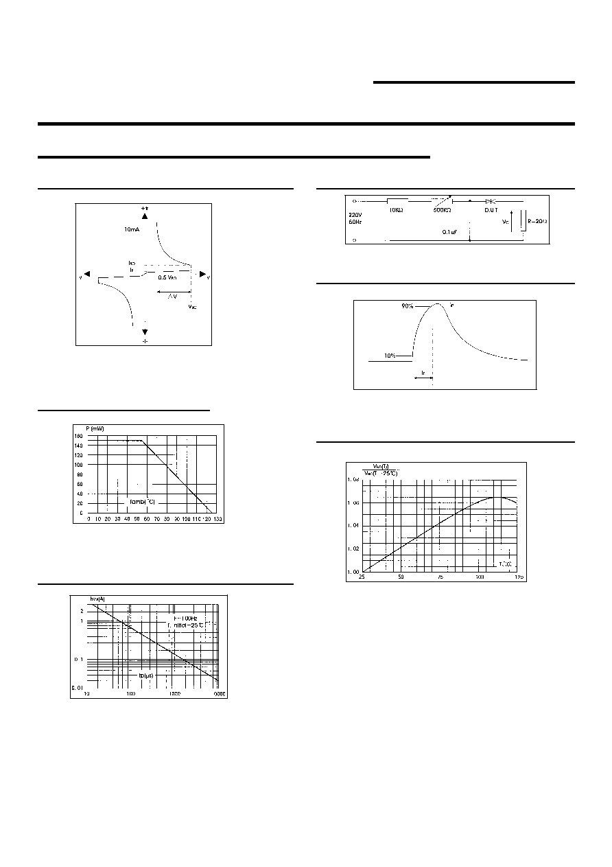
RATINGS AND CHARACTERISTIC CURVES DB3/DC34/DB4/DB6
DIAGRAM 1: Current-voltage charateristics
DIAGRAM 2: Test circuit for output voltage
DIAGRAM 3: Test circuit see diagram2 adjust R for
Ip=0.5A
FIG.1-Power disspation versus ambient
temperature(maximum values)
FIG.2-Relative variation of VBO versus juntion
temperature(typical values)
FIG.3-Peak pulse current versus pulse duration
(maximum values)
Copyright @ 2000 SHANGHAI CHENYI ELECTRONICS CO.,LTD
Page 2 of 2