-
+
-
+
V
FB
Signal
Common
Filter
20k
W
10k
W
Bias
Gnd
Detect
4.7k
W
50k
W
Amp
OUT
+V
S
SCR
Trigger
-
+
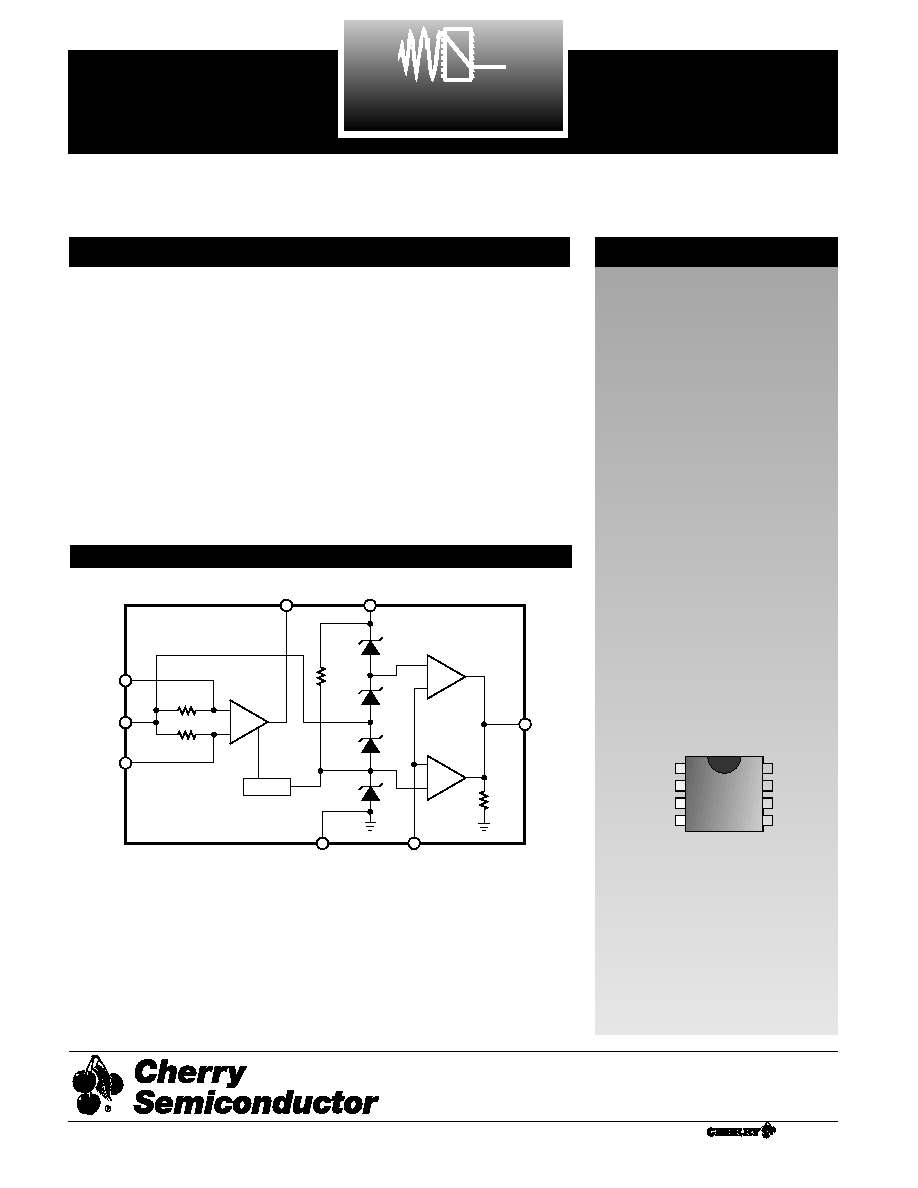
The CS294 is an AC outlet ground
fault interrupter controller IC. The
IC detects the presence of haz-
ardous grounding conditions and
open circuits the AC line before a
dangerous shock can occur.
The CS294 contains an operational
amplifier, an SCR driver and a 24V
zener shunt regulator. Two sense
coils, a bridge rectifier, a relay and
an SCR are required as external
components. The completed inter-
rupter circuit can detect and protect
against both hot wire to ground
faults and neutral wire to ground
faults.
The CS294 is built on a 30V bipolar
process and is available in 8 lead
DIP packages.
Features
s
Supply Derived from
AC Supply � 24V
s
Direct Interface to SCR
s
Adjustable Sensitivity
s
Grounded Neutral Fault
Detection
Package Options
CS294
Ground Fault Interrupter
CS294
Description
Block Diagram
1
V
FB
Filter
Signal Common
Gnd
Detect
Amp
OUT
+V
S
SCR Trigger
8 Lead PDIP & SO Narrow
1
Rev. 1/20/99
Cherry Semiconductor Corporation
2000 South County Trail, East Greenwich, RI 02818
Tel: (401)885-3600 Fax: (401)885-5786
Email: info@cherry-semi.com
Web Site: www.cherry-semi.com
A Company
�
V
FB
Error Amp Inverting Input
30V
-0.3V
N/A
20mA
Filter
Error Amp Non-Inverting Input
30V
-0.3V
1mA
1mA
Signal Common
Signal Reference Input
V(+V
S
) + 1V
V(+V
S
)
- 1V
1ma
1ma
Gnd
Power Supply Return
0V
0V
1mA
10mA
SCR Trigger
SCR Driver Output
30V
-0.3V
1mA
1mA
+V
S
Shunt Regulator Supply Input
30V
-0.3V
1mA
1mA
Amp
OUT
Error Amp Output
30V
-0.3V
1mA
1mA
Detect
Ground Fault Detect Input
6V
-0.3V
10mA
10mA
Electrical Characteristics:
T
A
= 25�C.
For ease of testing and improved test accuracy, Signal Common is grounded and a negative voltage is applied to the Gnd pin.
PARAMETER
TEST CONDITIONS
MIN
TYP
MAX
UNIT
CS294
2
Absolute Maximum Ratings
Pin Symbol
Pin Name
V
MAX
V
MIN
I
SOURCE
I
SINK
Operating Junction Temperature, T
J
. . . . . . . . . . . . . . . . . . . . . . . . . . . . . . . . . . . . . . . . . . . . . . . . . . . . . . . . . . . . . . . . . 150�C
Lead Temperature Soldering:
Wave Solder (through hole styles only) . . . . . . . . . . . . . . . . . . . . . . . . . . . . . . . . . . . . . . . . . . 10 Sec. max 260�C Peak
Reflow (SMD styles only) . . . . . . . . . . . . . . . . . . . . . . . . . . . . . . . . . . . . . . . . . . . 60 sec. max above 183�C, 230� peak
Storage Temperature Range, T
S
. . . . . . . . . . . . . . . . . . . . . . . . . . . . . . . . . . . . . . . . . . . . . . . . . . . . . . . . . . . . .
-65�C to 150�C
Supply Current
+V
S
1.2
mA
Negative Supply Voltage Clamp
-14.1
-11.9
-9.7
V
Positive Supply Voltage Clamp
9.7
11.9
14.1
V
Output Offset Voltage
-400
67
+1100
mV
Output Resistance
I(SCR Trigger) = 100�A
2.89
4.70
6.78
k�
Negative Amp Output Swing
-10.95
-8.5
V
Positive Amp Output Swing
8.5
11.5
V
Positive Detect Threshold
5.9
6.5
7.2
V
Negative Detect Threshold
-7.2
-6.5
-5.9
V
Detect Leakage Current
V(SCR Trigger) = 0V
0.5
5.0
�A
Amplifier Open Loop Gain
V(V
FB
) = 1mV RMS @ 50kHz
20
90
V/V
Operating Temperature Range T
A
(Note 1)
0
70
�C
Note 1: Guaranteed by design.

CS294
Package Pin Description
PACKAGE PIN #
PIN SYMBOL
FUNCTION
3
8 Lead PDIP
1
V
FB
The V
FB
pin is the inverting input to the on-chip operational
amplifier.
2
Filter
The Filter pin is the non-inverting input to the on-chip opera-
tional amplifier.
3
Signal Common
The Signal Common pin connects to +V
S
/2, to a 20k� resistor
tied to V
FB
and to a 10k� resistor tied to Filter.
4
Gnd
The Gnd pin is the power return terminal
5
SCR Trigger
The SCR Trigger pin drives the silicon controlled rectifier dur-
ing fault conditions. An internal 4.7k� resistor between this pin
and Gnd holds the SCR off in non-fault conditions.
6
+V
S
The +V
S
pin is the power input to the IC.
7
Amp
OUT
The Amp
OUT
pin is the output of the on-chip operational ampli-
fier.
8
Detect
The Detect pin is the fault detector input.

4
Rev. 1/20/99
Thermal Data
8 Lead
8 Lead
PDIP
SO Narrow
R
QJC
typ
52
45
�C/W
R
QJA
typ
100
165
�C/W
Package Specification
PACKAGE DIMENSIONS IN mm (INCHES)
PACKAGE THERMAL DATA
Ordering Information
Part Number
Description
CS294GN8
8 Lead PDIP
CS294GD8
8 Lead SO Narrow
CS294GDR8
8 Lead SO Narrow (tape & reel)
� 1999 Cherry Semiconductor Corporation
CS294
D
Lead Count
Metric
English
Max
Min
Max
Min
8 Lead PDIP
10.16
9.02
.400
.355
8 Lead SO Narrow
5.00
4.80
.197
.189
Cherry Semiconductor Corporation reserves the right to
make changes to the specifications without notice. Please
contact Cherry Semiconductor Corporation for the latest
available information.
Plastic DIP (N); 300 mil wide
0.39 (.015)
MIN.
2.54 (.100) BSC
1.77 (.070)
1.14 (.045)
D
Some 8 and 16 lead
packages may have
1/2 lead at the end
of the package.
All specs are the same.
.203 (.008)
.356 (.014)
REF: JEDEC MS-001
3.68 (.145)
2.92 (.115)
8.26 (.325)
7.62 (.300)
7.11 (.280)
6.10 (.240)
.356 (.014)
.558 (.022)
Surface Mount Narrow Body (D); 150 mil wide
1.27 (.050) BSC
0.51 (.020)
0.33 (.013)
6.20 (.244)
5.80 (.228)
4.00 (.157)
3.80 (.150)
1.57 (.062)
1.37 (.054)
D
0.25 (0.10)
0.10 (.004)
1.75 (.069) MAX
1.27 (.050)
0.40 (.016)
REF: JEDEC MS-012
0.25 (.010)
0.19 (.008)