
1
Features
V
CC
Gnd
OSC
V
FB
COMP
Sense
V
REF
V
OUT
Output
Enable
5V
Reference
Internal
Bias
NOR
S
R
PWM
Latch
Current
Sense
Comparator
Oscillator
1 V
R
2 R
V
C
Error
Amplifier
+
≠
2.50V
Set/
Reset
Undervoltage
Lock-out Circuit
34V
( ) Indicates CS-3843B
16V/10V
(8.4V/7.6V)
V
CC
Pwr
Pwr Gnd
REF
s
Very low Start Up Current
(300µA typ)
s
Optimized Off-line
Control
s
Internally Trimmed,
Temperature
Compensated Oscillator
s
Maximum Duty-cycle
Clamp
s
V
REF
stabilization before
Output Enable
s
Pulse-by-pulse Current
Limiting
s
Improved Undervoltage
Lockout
s
Double Pulse Suppression
s
1% Trimmed Bandgap
Reference
s
High Current Totem Pole
Output
Package Options
CS3842B/3843B
Off-Line Current Mode PWM Control Circuit
with Very Low Start Up Current
CS3842B/CS3843B
Description
Block Diagram
Absolute Maximum Ratings
Supply Voltage (I
CC
<30mA) ..........................................................Self Limiting
Supply Voltage (Low Impedance Source)...................................................30V
Output Current ...............................................................................................±1A
Output Energy (Capacitive Load) .................................................................5µJ
Analog Inputs (V
FB
, Sense) ............................................................-0.3V to 5.5V
Error Amp Output Sink Current...............................................................10mA
Lead Temperature Soldering
Wave Solder (through hole styles only) ...................10 sec. max, 260∞C peak
Reflow (SMD styles only) ....................60 sec. max above 183∞C, 230∞C peak
1
COMP
2
3
4
V
FB
Sense
OSC
V
REF
V
CC
V
OUT
Gnd
8
7
6
5
8 Lead PDIP & SO Narrow
10
7
14
13
12
8
1
2
3
4
5
6
11
9
COMP
NC
V
FB
NC
Sense
NC
OSC
V
REF
NC
V
CC
V
CC
Pwr
V
OUT
Pwr Gnd
Gnd
14L SO Narrow
Rev. 6/23/99
Cherry Semiconductor Corporation
2000 South County Trail, East Greenwich, RI 02818
Tel: (401)885-3600 Fax: (401)885-5786
Email: info@cherry-semi.com
Web Site: www.cherry-semi.com
A Company
Æ
The CS384XB provides all the neces-
sary features to implement off-line
fixed frequency current-mode control
with a minimum number of external
components. The family has been opti-
mized for very low start up current
(300µA, typ).
The CS384XB family incorporates a
precision temperature-controlled oscil-
lator with an internally trimmed dis-
charge current to minimize variations
in frequency. A precision duty-cycle
clamp eliminates the need for an exter-
nal oscillator when a 50% duty-cycle is
used. Duty-cycles of almost 100% are
possible. On board logic ensures that
VREF is stabilized before the output
stage is enabled. Ion-implant resistors
provide tighter control of undervoltage
lockout.
Other features include pulse-by-pulse
current limiting, and a high-current
totem pole output for driving capaci-
tive loads, such as the gate of a power
MOSFET. The output is LOW in the off
state, consistent with N-channel
devices.
These ICs are available in 8 and 14 lead
surface mount (SO) and 8 lead PDIP
packages.

2
Electrical Characteristics:
0T
A
70∞C, V
CC
=15V (Note 1); R
T
=680, C
T
=.022µF for triangular mode,
R
T
=10k, C
T
=3.3nF for sawtooth mode (see Fig. 3), unless otherwise stated
PARAMETER
TEST CONDITIONS
MIN
TYP
MAX
UNITS
CS3842B/3843B
s
Reference Section
Output Voltage
T
J
=25∞C, I
OUT
=1mA
4.90
5.00
5.10
V
Line Regulation
12V
IN
25V
6
20
mV
Load Regulation
1I
OUT
20mA
6
25
mV
Temperature Stability
(Note 2)
0.2
0.4
mV/∞C
Total Output Variation
Line, Load, Temperature (Note 2)
4.82
5.18
V
Output Noise Voltage
10Hzf10kHz, T
J
=25∞C (Note 2)
50
µV
Long Term Stability
T
A
=125∞C, 1kHrs. (Note 2)
5
25
mV
Output Short Circuit
T
A
=25∞C
-30
-100
-180
mA
s
Oscillator Section
Initial Accuracy
Sawtooth Mode (see Fig. 3), T
J
=25∞C
47
52
57
kHz
Triangular Mode (see Fig. 3), T
J
=25∞C
44
52
60
kHz
Voltage Stability
12V
CC
25V
0.2
1.0
%
Temp. Stability
Sawtooth Mode T
MIN
T
A
T
MAX
(Note 2)
5
%
Triangular Mode T
MIN
T
A
T
MAX
(Note 2)
8
%
Amplitude
Oscillator peak to peak
1.7
V
Discharge Current
T
J
=25∞C
7.5
8.3
9.3
mA
T
MIN
T
A
T
MAX
7.2
9.5
mA
s
Error Amp Section
Input Voltage
V
COMP
=2.5V
2.42
2.50
2.58
V
Input Bias Current
-0.3
-2.0
µA
A
VOL
2V
OUT
4V
65
90
dB
Unity Gain Bandwidth
(Note 2)
0.7
1.0
MHz
PSRR
12V
CC
25V
60
70
dB
Output Sink Current
V
FB
=2.7V, V
OSC
=1.1V
2
6
mA
Output Source Current
V
FB
=2.3V, V
OSC
=5V
-0.5
-0.8
mA
V
OUT
High
V
FB
=2.3V, R
L
=15k to ground
5
6
V
V
OUT
Low
V
FB
=2.7V, R
L
=15k to V
REF
0.7
1.1
V
s
Current Sense Section
Gain
(Notes 3 & 4)
2.85
3.00
3.15
V/V
Maximum Input Signal
V
COMP
=5V (Note 3)
0.9
1.0
1.1
V
PSRR
12V
CC
25V (Note 3)
70
dB
Input Bias Current
-2
-10
µA
Delay to Output
T
J
=25∞C (Note 2)
150
300
ns
s
Output Section
Output Low Level
I
SINK
=20mA
0.1
0.4
V
I
SINK
=200mA
1.5
2.2
V
Output High Level
I
SOURCE
=20mA
13.0
13.5
V
I
SOURCE
=200mA
12.0
13.5
V

3
CS3842B/3843B
Electrical Characteristics: continued
PARAMETER
TEST CONDITIONS
MIN
TYP
MAX
UNITS
CS-3842B
CS-3843B
PARAMETER
TEST CONDITIONS
MIN
TYP MAX
MIN
TYP
MAX UNITS
Notes: 1. Adjust V
CC
above the start threshold before setting at 15V.
2. These parameters, although guaranteed, are not 100% tested
in production.
3. Parameter measured at trip point of latch with V
FB
=0.
4. Gain defined as:
A =
; 0 V
Sense
0.8V.
V
COMP
V
Sense
Package Pin Description
PACKAGE PIN #
PIN SYMBOL
FUNCTION
8L PDIP/SO
14L SO Narrow
1
1
COMP
Error amp output, used to compensate error amplifier
2
3
V
FB
Error amp inverting input
3
5
Sense
Noninverting input to Current Sense Comparator
4
7
OSC
Oscillator Timing Network with Capacitor to Ground, resistor
to V
REF
5
8
Gnd
Ground
9
Pwr Gnd
Output driver Ground
6
10
V
OUT
Output drive pin
11
V
CC
Pwr
Output driver positive supply
7
12
V
CC
Positive power supply
8
14
V
REF
Output of 5V internal reference
2,4,6,13
NC
No Connection
s
Output Section: continued
Rise Time
T
J
=25∞C, C
L
=1nF (Note 2)
50
150
ns
Fall Time
T
J
=25∞C, C
L
=1nF (Note 2)
50
150
ns
Output Leakage
UVLO Active, V
OUT
=0
-0.01
-10.00
µA
s
Total Standby Current
Start-Up Current
0.3
0.5
mA
Operating Supply Current
V
FB
=V
Sense
=0V R
T
=10k, C
T
=3.3nF
11
17
mA
V
CC
Zener Voltage
I
CC
=25mA
34
V
s
Under-Voltage Lockout Section
Start Threshold
14.5
16.0
17.5
7.8
8.4
9.0
V
Min. Operating
After Turn On
8.5
10.0
11.5
7.0
7.6
8.2
V
Voltage
Undervoltage Lockout
During Undervoltage Lockout (Figure 1), the output driv-
er is biased to a high impedance state. V
OUT
should be
shunted to ground with a resistor to prevent output leak-
age current from activating the power switch.
PWM Waveform
To generate the PWM waveform, the control voltage from
the error amplifier is compared to a current sense signal
which represents the peak output inductor current
(Figure 2). An increase in V
CC
causes the inductor current
slope to increase, thus reducing the duty cycle. This is an
inherent feed-forward characteristic of current mode con-
trol, since the control voltage does not have to change
during changes of input supply voltage.
When the power supply sees a sudden large output cur-
rent increase, the control voltage will increase allowing
the duty cycle to momentarily increase. Since the duty
4
CS3842B/3843B
Test Circuit
V
REF
V
CC
V
OUT
1k
1W
0.1
µ
F
0.1
µ
F
V
REF
V
CC
V
OUT
Gnd
V
FB
Sense
OSC
COMP
5k
100k
4.7k
1k
ERROR AMP
ADJUST
4.7k
Sense
ADJUST
R
T
2N2222
C
T
Gnd
A
CS-3842B
CS-3843B
Circuit Description
Typical Performance Characteristics:
Oscillator Duty Cycle vs R
T
Oscillator Frequency vs C
T
V
CC
ON/OFF Command
to reset of IC
V
ON
16V 8.4V
V
OFF
10V 7.6V
CS3842B CS3843B
<0.5mA
<15mA
V
ON
V
OFF
I
CC
V
CC
Figure 1: Typical Undervoltage Characteristics
.0005
.001
.002
.003
.005
.01
.02
.03 .04
800
900
FREQ. (kHz)
C
T
(
µ
F)
700
600
500
400
300
200
100
.05
R
T
=1.5k
R
T
=680
R
T
=10k
100
200
700
1k
2k
5k
7k
10k
80
90
DUTY
CYCLE (%)
R
T
(
)
70
60
50
40
30
20
10
4k
3k
500
400
300
100

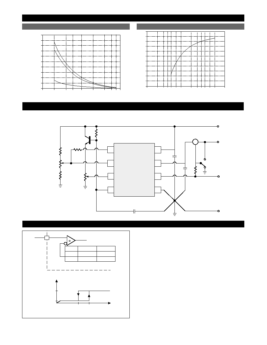
Figure 3: Oscillator Timing Network and parameters
V
REF
OSC
Gnd
R
T
C
T
V
OSC
Internal Clock
LARGE R
T
(
10k
)
V
REF
Internal Clock
SMALL R
T
(
700k
)
5
CS3842B/3843B
Figure 3: Oscillator
Sawtooth Mode
Triangular Mode
V
upper
V
lower
t
c
t
d
Figure 2: Timing Diagram for key CS-384XB parameters
V
CC
I
OUT
V
OUT
Switch
Current
EA Output
V
OSC
OSC
RESET
cycle tends to exceed the maximum allowed, to prevent
transformer saturation in some power supplies, the inter-
nal oscillator waveform provides the maximum duty cycle
clamp as programmed by the selection of oscillator timing
components.
Setting the Oscillator
The oscillator timing capacitor, C
T
, is charged by V
REF
through R
T
and discharged by an internal current source
(Figure 3). During the discharge time, the internal clock
signal blanks out the output to the Low state, thus provid-
ing a user selected maximum duty cycle clamp.
Charge and discharge times are determined by the general
formulas:
t
c
= R
T
C
T
ln
t
d
= R
T
C
T
ln
Substituting in typical values for the parameters in the
above formulas:
V
REF
= 5.0V, V
upper
= 2.7V, V
lower
= 1.0V, I
d
= 8.3mA,
then
t
c
0.5534R
T
C
T
t
d
= R
T
C
T
ln
The frequency and maximum duty cycle can be deter-
mined from the Typical Performance Characteristics
graphs.
Grounding
High peak currents associated with capacitive loads neces-
sitate careful grounding techniques. Timing and bypass
capacitors should be connected close to ground in a single
point ground.
The transistor and 5k potentiometer are used to sample
the oscillator waveform and apply an adjustable ramp to
Sense.
)
2.3 ≠ 0.0083 R
T
4.0 ≠ 0.0083 R
T
(
)
V
REF
≠ I
d
R
T
≠V
lower
V
REF
≠ I
d
R
T
≠ V
upper
(
)
V
REF
≠ V
lower
V
REF
≠ V
upper
(