1
Features
SINE-
SINE+
Gnd
V
REG
F/V
OUT
SINE
Output
COS
Output
V
REG
7.0V
V
CC
COS-
COS+
Gnd
Gnd
FREQ
IN
SQ
OUT
CP+
Input
Comp.
–
+
–
+
Gnd
CP-
Voltage
Regulator
+
–
+
–
High Voltage
Protection
Charge Pump
BIAS
Func.
Gen.
F
GEN
+
–
+
–
s
Direct Sensor Input
s
High Output Torque
s
Low Pointer Flutter
s
High Input Impedance
s
Overvoltage Protection
Package Option
20 Lead PDIP
CS4101
Precision Air-Core Tach/Speedo Driver
with Separate Function Generator Input
1
CP+
2
3
4
5
6
7
8
SQ
OUT
FREQ
IN
BIAS
Gnd
Gnd
NC
COS+
16
15
14
13
12
11
10
CP-
F/V
OUT
V
REG
NC
Gnd
Gnd
NC
SIN+
9
COS-
SIN-
17
18
V
CC
F
GEN
19
20
CS4101
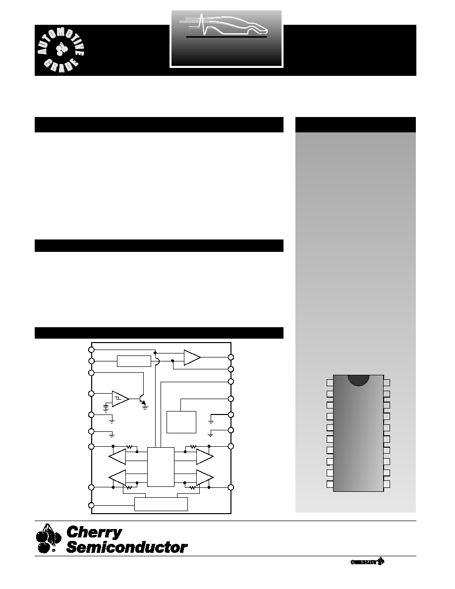
Description
The CS4101 is specifically designed
for use with air-core meter move-
ments. The IC provides all the func-
tions necessary for an analog
tachometer or speedometer. The
CS4101 takes a speed sensor input
and generates sine and cosine relat-
ed output signals to differentially
drive an air-core meter.
Many enhancements have been
added over industry standard
tachometer drivers such as the
CS-289 or LM1819. The output uti-
lizes differential drivers which elim-
inates the need for a zener reference
and offers more torque. The device
withstands 60V transients which
decreases the protection circuitry
required. The device is also more
precise than existing devices allow-
ing for fewer trims and for use in a
speedometer.
Block Diagram
Absolute Maximum Ratings
Supply Voltage (<100ms pulse transient) .........................................V
CC
= 60V
(continuous)..............................................................V
CC
= 24V
Operating Temperature .............................................................–40°C to +105°C
Storage Temperature..................................................................–40°C to +165°C
Junction Temperature .................................................................–40°C to+150°C
ESD (Human Body Model) .............................................................................4kV
Lead Temperature Soldering
Wave Solder(through hole styles only).............10 sec. max, 260°C peak
Rev 11/20/98
Cherry Semiconductor Corporation
2000 South County Trail, East Greenwich, RI 02818
Tel: (401)885-3600 Fax: (401)885-5786
Email: info@cherry-semi.com
Web Site: www.cherry-semi.com
A Company
®
2
Electrical Characteristics:
-40°C ≤ T
A
≤ 85°C, 8.5V ≤ V
CC
≤ 15V unless otherwise specified.
PARAMETER
TEST CONDITIONS
MIN
TYP
MAX
UNIT
CS4101
s Supply Voltage Section
I
CC
Supply Current
V
CC
= 16V, -40°C, No Load
50
125
mA
V
CC
Normal Operation Range
8.5
13.1
16.0
V
s Input Comparator Section
Positive Input Threshold
2.4
3.4
4.4
V
Input Hysteresis
200
400
mV
Input Bias Current *
0V ≤ V
IN
≤ 8V -10
-80
µA
Input Frequency Range
0
20
KHz
Input Voltage Range
in series with 1kΩ
-1
V
CC
V
Output V
SAT
I
CC
= 10mA
0.15
0.40
V
Output Leakage
V
CC
= 7V
10
µA
Low V
CC
Disable Threshold
7.0
8.0
8.5
V
Logic 0 Input Voltage
2.4
V
*Note: Input is clamped by an internal 12V Zener.
s Voltage Regulator Section
Output Voltage
6.25
7.00
7.50
V
Output Load Current
10
mA
Output Load Regulation
0 to 10 mA
10
50
mV
Output Line Regulation
8.5V ≤ V
CC
≤ 16V
20
150
mV
Power Supply Rejection
V
CC
= 13.1V, 1Vp/p 1kHz
34
46
dB
s Charge Pump Section
Inverting Input Voltage
1.5
2.0
2.5
V
Input Bias Current
40
150
nA
V
bias
Input Voltage
1.5
2.0
2.5
V
Non Invert. Input Voltage
I
IN
= 1mA
0.7
1.1
V
Linearity*
@ 0, 87.5, 175, 262.5, + 350Hz
-0.10
0.28
+0.70
%
F/V
OUT
Gain
@ 350Hz, C
T
= 0.0033µF, R
T
= 243kΩ
7
10
13
mV/Hz
Norton Gain, Positive
I
IN
= 15µA
0.9
1.0
1.1
I/I
Norton Gain, Negative
I
IN
= 15µA
0.9
1.0
1.1
I/I
*Note: Applies to % of full scale (270°).
s Function Generator Section: -40° ≤ T
A
≤ 85°C, V
CC
= 13.1V unless otherwise noted.
Differential Drive Voltage
8.5V ≤ V
CC
≤ 16V
5.5
6.5
7.5
V
(V
COS
+ - V
COS
-)
Q = 0°
Differential Drive Voltage
8.5V ≤ V
CC
≤ 16V
5.5
6.5
7.5
V
(V
SIN
+ - V
SIN
-)
Q = 90°
Differential Drive Voltage
8.5V ≤ V
CC
≤ 16V
-7.5
-6.5
-5.5
V
(V
COS
+ - V
COS
-)
Q = 180°
Differential Drive Voltage
8.5V ≤ V
CC
≤ 16V
-7.5
-6.5
-5.5
V
(V
SIN
+ - V
SIN
-)
Q = 270°
Differential Drive Current
8.5V ≤ V
CC
≤ 16V
33
42
mA
Zero Hertz Output Angle
-1.5
0.0
1.5
deg
Function Generator Error *
V
CC
= 13.1V
-2
0
+2
deg
Reference Figures 1,2,3,4
Q = 0° to 305°
* Note: Deviation from nominal per Table 1 after calibration at 0 and 270°.

3
PACKAGE LEAD #
LEAD SYMBOL
FUNCTION
CS4101
Electrical Characteristics:
continued
PARAMETER
TEST CONDITIONS
MIN
TYP
MAX
UNIT
s Function Generator Section: continued
Function Generator Error
13.1V ≤ V
CC
≤ 16V
-2.5
0
+2.5
deg
Function Generator Error
13.1V ≤ V
CC
≤ 11V
-1
0
+1
deg
Function Generator Error
13.1V ≤ V
CC
≤ 9V
-3
0
+3
deg
Function Generator Error
25°C ≤ T
A
≤ 80°C
-3
0
+3
deg
Function Generator Error
25°C ≤ T
A
≤ 105°C
-5.5
0
+5.5
deg
Function Generator Error
–40°C ≤ T
A
≤ 25°C
-3
0
+3
deg
Function Generator Gain
T
A
= 25°C
Q vs F/V
OUT
60
77
95
°/V
Package Lead Description
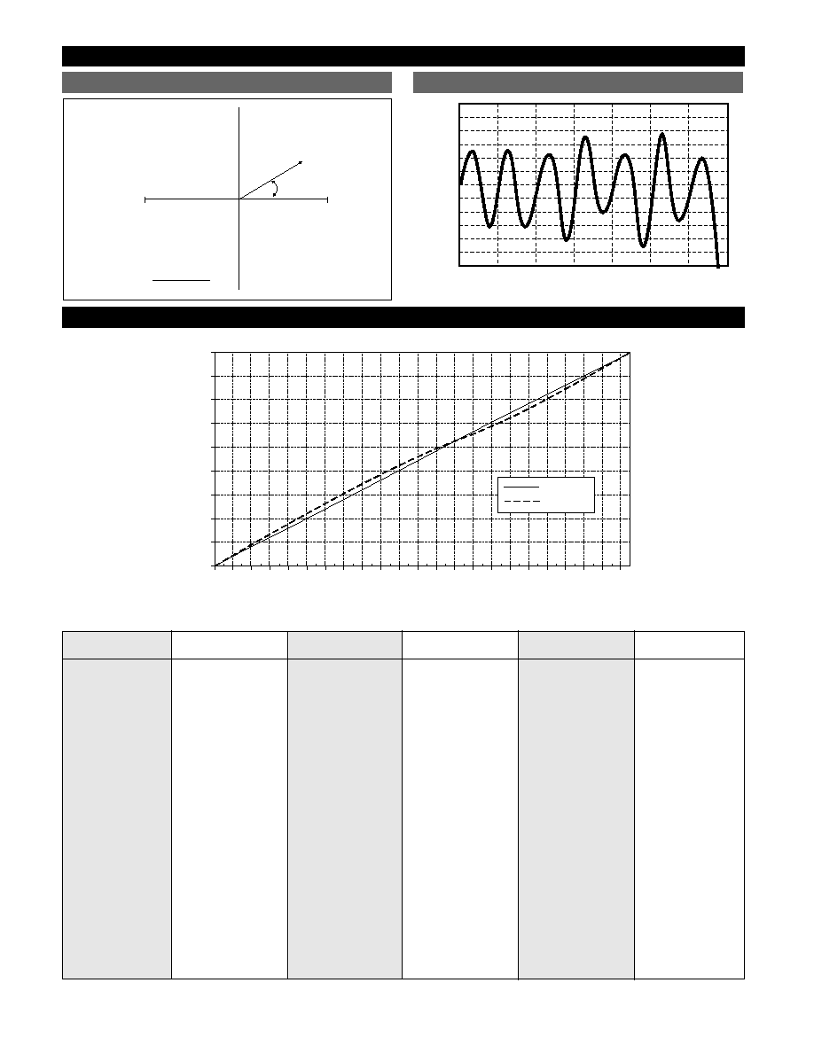
Typical Performance Characteristics
0
45
90
135
180
225
270
315
Output V
oltage (V)
Degrees of Deflection (
∞)
7
6
5
4
3
2
1
0
-1
-2
-3
-4
-5
-6
-7
COS
SIN
0
45
90
135
180
225
270
315
F/V Output (V)
Frequency/Output Angle (
∞)
7
6
5
4
3
2
1
0
Figure 2: Charge Pump Output Voltage vs Output Angle
Figure 1: Function Generator Output Voltage
vs Degrees of Deflection
F/V
OUT
= 2.0V + 2 FREQ
¥ C
T
¥ R
T
¥ (V
REG
- 0.7)
20L
1
CP+
Positive input to charge pump.
2
SQ
OUT
Buffered square wave output signal.
3
FREQ
IN
Speed or rpm input signal.
4
BIAS
Test point or Zero adjustment.
5, 6, 15, 16
Gnd
Ground Connections.
7, 14, 17
NC
No Connection.
8
COS+
Positive cosine output signal.
9
COS-
Negative cosine output signal.
10
V
CC
Ignition or battery supply voltage.
11
F
GEN
Function generator input signal.
12
SIN-
Negative sine output signal.
13
SIN+
Positive sine output signal.
18
V
REG
Voltage regulator output.
19
F/V
OUT
Output voltage proportional to input signal frequency.
20
CP-
Negative input to charge pump.
4
Typical Performance Characteristics continued
CS4101
Nominal Angle vs. Ideal Angle (After calibrating at 180°)
+7V
–7V
(V
COS+
) - (V
COS-
)
7V
Angle
-7V
Q
(V
SINE+
) - (V
SINE-
)
]
V
SIN+
– V
SIN-
V
COS+
– V
COS-
Q = ARCTAN
[
-1.50
Deviation (
∞
)
0
45
90
135
180
225
270
315
-1.25
-1.00
-0.75
-0.50
-0.25
0.00
0.25
0.50
0.75
1.00
1.25
1.50
Theoretical Angle (
∞)
Figure 4: Nominal Output Deviation
Figure 3: Output Angle in Polar Form
Ideal Angle
(Degrees)
Nominal Angle (Degrees)
0
5
10
15
20
25
30
35
40
45
1
5
9
13
17
21
25
29
33
37
41
45
Ideal Degrees
Nominal Degrees
0
0
1
1.09
2
2.19
3
3.29
4
4.38
5
5.47
6
6.56
7
7.64
8
8.72
9
9.78
10
10.84
11
11.90
12
12.94
13
13.97
14
14.99
15
16.00
16
17.00
17
17.98
18
18.96
19
19.92
20
20.86
21
21.79
22
22.71
23
23.61
24
24.50
25
25.37
26
26.23
27
27.07
28
27.79
29
28.73
30
29.56
31
30.39
32
31.24
33
32.12
34
33.04
35
34.00
36
35.00
37
36.04
38
37.11
39
38.21
40
39.32
41
40.45
42
41.59
43
42.73
44
43.88
45
45.00
50
50.68
55
56.00
60
60.44
65
64.63
70
69.14
75
74.00
80
79.16
85
84.53
90
90.00
95
95.47
100
100.84
105
106.00
110
110.86
115
115.37
120
119.56
125
124.00
130
129.32
135
135.00
140
140.68
145
146.00
150
150.44
155
154.63
160
159.14
165
164.00
170
169.16
175
174.33
180
180.00
185
185.47
190
190.84
195
196.00
200
200.86
205
205.37
210
209.56
215
214.00
220
219.32
225
225.00
230
230.58
235
236.00
240
240.44
245
244.63
250
249.14
255
254.00
260
259.16
265
264.53
270
270.00
275
275.47
280
280.84
285
286.00
290
290.86
295
295.37
300
299.21
305
303.02
Ideal
Q
Nominal
Ideal
Q
Nominal
Ideal
Q
Nominal
Ideal
Q
Nominal
Ideal
Q
Nominal
Ideal
Q
Nominal
Degrees
Q Degrees
Degrees
Q Degrees
Degrees
Q Degrees
Degrees
Q Degrees
Degrees
Q Degrees
Degrees
Q Degrees
Table 1:
Function Generator Output Nominal Angle vs. Ideal Angle (After calibrating at 270°)
Note:
Temperature, voltage and nonlinearity not included.
Note:
Temperature, voltage and nonlinearity not included.

5
CS4101
The CS4101 is specifically designed for use with air-core
meter movements. It includes an input comparator for
sensing an input signal from an ignition pulse or speed
sensor, a charge pump for frequency to voltage conver-
sion, a bandgap voltage regulator for stable operation,
and a function generator with sine and cosine amplifiers
to differentially drive the motor coils.
From the simplified block diagram of Figure 5A, the
input signal is applied to the FREQ
IN
lead, this is the
input to a high impedance comparator with a typical pos-
itive input threshold of 3.4V and typical hysteresis of
0.4V. The output of the comparator, SQ
OUT
, is applied to
the charge pump input CP+ through an external capaci-
tor C
T
. When the input signal changes state, C
T
is
charged or discharged through R3 and R4. The charge
accumulated on C
T
is mirrored to C
4
by the Norton
Amplifier circuit comprising Q1, Q2 and Q3. The charge
pump output voltage, F/V
OUT
, ranges from 2V to 6.3V
depending on the input signal frequency and the gain of
the charge pump according to the formula:
F/V
OUT
= 2.0V + 2
¥ FREQ ¥ C
T
¥ R
T
¥ (V
REG
– 0.7V)
R
T
is a potentiometer used to adjust the gain of the F/V
output stage and give the correct meter deflection. The
F/V output voltage is applied to the function generator
input lead, F
GEN
. An additional filter circuit can be added
between F/V
OUT
and F
GEN
to reduce needle flutter. The
output voltage of the sine and cosine amplifiers are
derived from the on-chip amplifier and function genera-
tor circuitry. The various trip points for the circuit (i.e., 0°,
90°, 180°, 270°) are determined by an internal resistor
divider, and the bandgap voltage reference. The coils are
differentially driven, allowing bidirectional current flow
in the outputs, thus providing up to 305° range of meter
deflection. Driving the coils differentially offers faster
response time, higher current capability, higher output
voltage swings, and reduced external component count.
The key advantage is a higher torque output for the
pointer.
The output angle,
Q, is equal to the F/V gain multiplied
by the function generator gain:
Q = A
F/V
¥ A
FG
,
where:
A
FG
= 77°/V (typ)
The relationship between input frequency and output
angle is:
Q = A
FG
¥ 2 ¥ FREQ ¥ C
T
¥ R
T
¥ (V
REG
– 0.7V)
or,
Q = 970 ¥ FREQ ¥ C
T
¥ R
T
The ripple voltage at the F/V converter’s output is deter-
mined by the ratio of C
T
and C4 in the formula:
∆V =
Ripple voltage on the F/V output causes pointer or nee-
dle flutter especially at low input frequencies.
The response time of the F/V is determined by the time
constant formed by R
T
and C4. Increasing the value of C4
will reduce the ripple on the F/V output but will also
increase the response time. An increase in response time
causes a very slow meter movement and may be unac-
ceptable for many applications.
Design Example
Maximum meter Deflection = 270°
Maximum Input Frequency = 350Hz
1. Select R
T
and C
T
Q = A
GEN
¥ ∆
F/V
∆
F/V
= 2
¥ FREQ ¥ C
T
¥ R
T
¥ (V
REG
– 0.7V)
Q = 970 ¥ FREQ ¥ C
T
¥ R
T
Let C
T
= 0.0033µF, Find R
T
R
T
=
R
T
= 243kΩ
R
T
should be a 250kΩ potentiometer to trim out any inac-
curacies due to IC tolerances or meter movement pointer
placement.
2. Select R3 and R4
Resistor R3 sets the output current from the voltage regu-
lator. The maximum output current from the voltage reg-
ulator is 10mA R
3
must ensure that the current does not
exceed this limit.
Choose R3 = 3.3kΩ
The charge current for C
T
is:
= 1.90mA
C
1
must charge and discharge fully during each cycle of
the input signal. Time for one cycle at maximum frequen-
cy is 2.85ms. To ensure that C
T
is discharged, assume that
the (R3 + R4) C
T
time constant is less than 10% of the
minimum input frequency pulse width.
T = 285µs
Choose R4 = 1kΩ.
Charge time:
T = R3
¥ C
T
= 3.3kΩ
¥ 0.0033µF = 10.9µs
Discharge time:T = (R3 + R4)C
T
= 4.3kΩ
¥ 0.0033µF = 14.2µs
3. Determine C4
C4 is selected to satisfy both the maximum allowable rip-
ple voltage and response time of the meter movement.
C4 =
With C4 = 0.47µF, the F/V ripple voltage is 44mV.
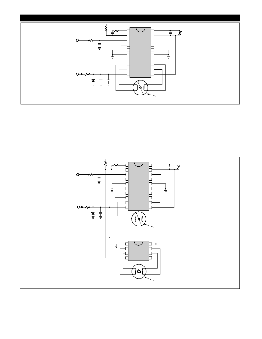
Figure 7 shows how the CS4101 and the CS-8441 are used
to produce a speedometer and odometer circuit.
C
T
(V
REG
– 0.7V)
V
RIPPLE(MAX)
V
REG
– 0.7V
3.3kΩ
270°
970
¥ 350Hz ¥ 0.0033µF
C
T
(V
REG
– 0.7V)
C4
Circuit Description and Application Notes
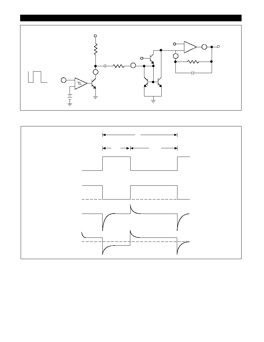
6
CS4101
Circuit Description and Application Notes: continued
+
–
R
T
C4
CP–
+
–
F/V
OUT
F to V
2.0V
Q2
Q1
Q3
0.25V
CP+
R4
C
T
V
C
(t)
+ –
R3
V
REG
SQ
OUT
Q
SQUARE
3.4V
FREQ
IN
T
PW
T-PW
FREQ
IN
I
CP+
SQ
OUT
V
CC
V
REG
0
0
0
V
CP+
Figure 5A: Partial Schematic of Input and Charge Pump
Figure 5B: Timing Diagram of FREQ
IN
and I
CP
7
Speedometer/Odometer or Tachometer Application
10
1
CP+
2
3
4
5
6
7
8
SQ
OUT
FREQ
IN
Gnd
Gnd
SIN+
COS+
NC
20
19
18
17
16
15
14
13
CP-
F/V
OUT
V
REG
NC
Gnd
Gnd
NC
BIAS
CS4101
C
T
R3
C3
C1
D2
R1
D1
+
C4
R
T
COSINE
SINE
Air Core
Gauge
200
W
Speedometer
Battery
Speedo
Input
C2
R2
R4
CP+
9
COS-
V
CC
12
11
SINE-
F
GEN
C
T
R3
C3
C1
D2
R1
D1
+
C4
R
T
COSINE
SINE
Air Core
Gauge
200
W
Speedometer
Battery
Speedo
Input
R2
R4
1
CS8441
C2
Air Core
Stepper Motor
200
W
Odometer
10
1
CP+
2
3
4
5
6
7
8
SQ
OUT
FREQ
IN
Gnd
Gnd
SIN+
COS+
NC
20
19
18
17
16
15
14
13
CP-
F/V
OUT
V
REG
NC
Gnd
Gnd
NC
BIAS
CS4101
CP+
9
COS-
V
CC
12
11
SINE-
F
GEN
CS4101
R1 - 3.9, 500mW
R2 - 10kΩ
R3 - 3kΩ
R4 - 1kΩ
R
T
- Trim Resistor +/- 20 PPM/DEG. C
C1 - 0.1µF
C2 - 1. Stand alone Speedo or Tach "0" µF
2. Stand alone Speedo or Tach with return to Zero, 2000µF
3. With CS-8441 application, 10µF
C3 - 0.1µF
C4 - 0.47µF
C
T
- 0.0033µF, +/- 30 PPM/°C
D1 - 1A, 600 PIV
D2 - 50V, 500mW Zener
Note 1: For 58% Speed Input
T
MAX
≤ 5/f
MAX
where
T
MAX
= C
T
(R3+R4)
f
MAX
= maximum speed input frequency
Note 1: The product of C
T
and R
T
have a direct effect on
gain and therefore directly effect temperature
compensation
Note 2: C4 Range; 20pF to .2µF
Note 3: R4 Range; 100kΩ to 500kΩ
Note 4: The IC must be protected from transients above
60V and reverse battery conditions
Note 5: Additional filtering on the FREQ
IN
lead may be
required
Figure 6
Figure 7
8
Rev. 11/20/98
CS4101
Part Number
Description
CS4101EN20
20L PDIP
D
Lead Count
Metric
English
Max
Min
Max
Min
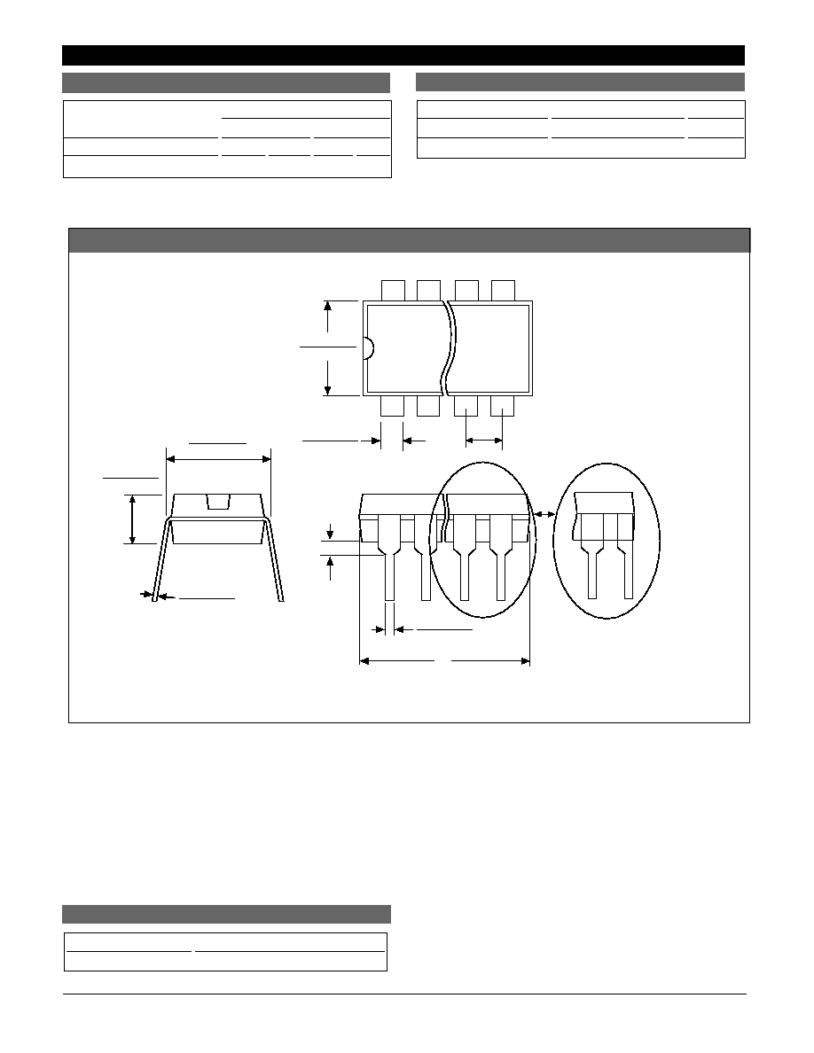
20 Lead PDIP
26.92 24.89
1.060 .980
Ordering Information
Thermal Data
20L PDIP
R
QJC
typ
25
˚C/W
R
QJA
typ
65
˚C/W
Package Specification
PACKAGE DIMENSIONS IN mm (INCHES)
PACKAGE THERMAL DATA
© 1999 Cherry Semiconductor Corporation
Cherry Semiconductor Corporation reserves the
right to make changes to the specifications without
notice. Please contact Cherry Semiconductor
Corporation for the latest available information.
Plastic DIP (N); 300 mil wide
0.39 (.015)
MIN.
2.54 (.100) BSC
1.77 (.070)
1.14 (.045)
D
Some 8 and 16 lead
packages may have
1/2 lead at the end
of the package.
All specs are the same.
.203 (.008)
.356 (.014)
REF: JEDEC MS-001
3.68 (.145)
2.92 (.115)
8.26 (.325)
7.62 (.300)
7.11 (.280)
6.10 (.240)
.356 (.014)
.558 (.022)