1
Features
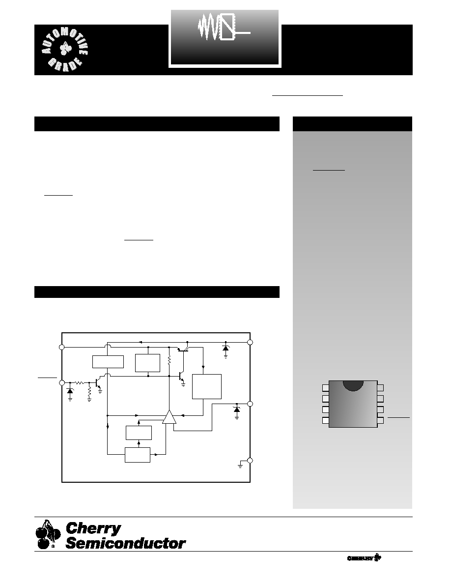
Error
Amplifier
Thermal
Shutdown
Over
Voltage
Shutdown
V
IN
Gnd
V
OUT
Bandgap
Reference
+ -
Current Limit
Sense
Current Source
(Circuit Bias)
Adj
ENABLE
Input
s
Low Quiescent Current
s
Adjustable Output:
5V to 12V
s
for Sleep Mode
Control
s
100mA Output Current
Capability
s
Fault Protection
+60V Load Dump
-15V Reverse Voltage
Short Circuit
Thermal Shutdown
s
Low Reverse Current
(Output to Input)
ENABLE
Package Options
CS8271
CS8271
Description
The CS8271 is an adjustable microp-
ower voltage regulator with very
low quiescent current (60µA typical
at 100µA load). The output supplies
100mA of load current with a maxi-
mum dropout voltage of only
600mV. Control logic includes
. The combination of low
quiescent current, outstanding reg-
ulator performance and control
logic makes the CS8271 ideal for
any battery operated equipment.
The logic level compatible
pin allows the user to put the regu-
lator into a shutdown mode where it
draws only 50µA of quiescent cur-
rent.
The regulator is protected against
reverse battery, short circuit, over
voltage, and over temperature con-
ditions. The device can withstand
60V load dump transients making it
suitable for use in automotive envi-
ronments.
The CS8271 is pin compatible with
the National Semiconductor
LM2931.
ENABLE
ENABLE
Block Diagram
1
V
OUT
Gnd
NC
Adj
V
IN
NC
NC
ENABLE
Other Packages: Consult factory for
16L SO Batwing, 5L TO-220 and D
2
PAK.
8L SOIC & PDIP
Adjustable Micropower Low Dropout
Linear Regulator with ENABLE
A Company
®
Rev. 3/26/97
Cherry Semiconductor Corporation
2000 South County Trail, East Greenwich, RI 02818
Tel: (401)885-3600 Fax: (401)885-5786
Email: info@cherry-semi.com
Web Site: www.cherry-semi.com
2
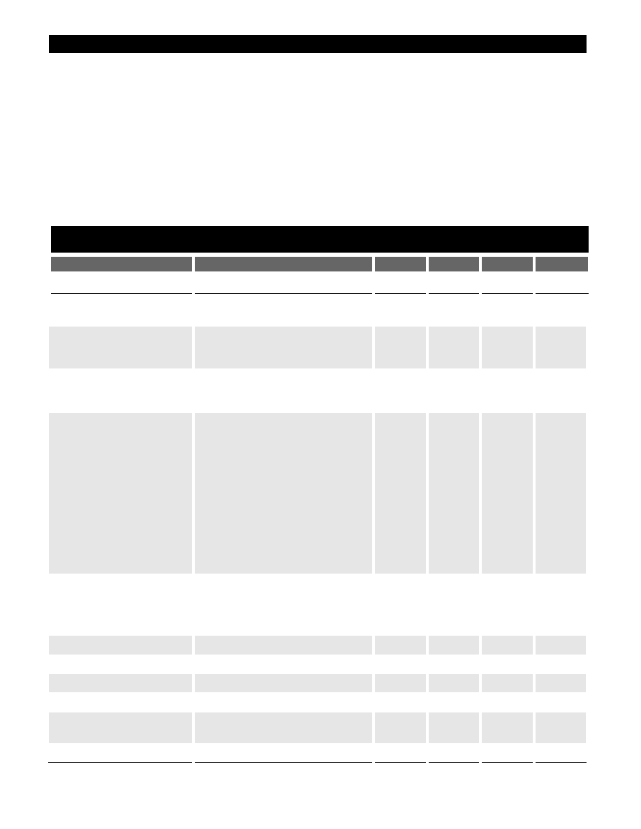
Power Dissipation.............................................................................................................................................Internally Limited
Transient Input Voltage ..................................................................................................................................................-50V, 60V
Reverse Battery..........................................................................................................................................................................-15V
Output Current .................................................................................................................................................Internally Limited
ESD Susceptibility (Human Body Model)..............................................................................................................................2kV
Junction Temperature .............................................................................................................................................-40°C to 150°C
Storage Temperature...............................................................................................................................................-55°C to 150°C
Lead Temperature Soldering
Wave Solder (through hole styles only) .....................................................................................10 sec. max, 260°C peak
Reflow (SMD styles only) ......................................................................................60 sec. max above 183°C, 230°C peak
Adj and Enable Output ..................................................................................................................................................-0.3V, 10V
V
OUT
...........................................................................................................................................................................-0.3V, 20V
PARAMETER
TEST CONDITIONS
MIN
TYP
MAX
UNIT
Absolute Maximum Ratings
Electrical Characteristics:
V
OUT
+ 1V ≤ V
IN
≤ 30V, 5V ≤ V
OUT
≤ 12V, I
OUT
= 10mA, -40° ≤ T
A
≤ 125°, -40° ≤ T
J
≤ 150°,
V
ENABLE
= 0V; unless otherwise specified.
CS8271
s Output Voltage
Dropout Voltage
I
OUT
= 100µA, V
DROP
= (V
IN
– V
OUT
)
100
150
mV
I
OUT
= 100mA, V
DROP
= (V
IN
– V
OUT
)
400
600
mV
Load Regulation
Measure V
OUT
when 0.1
1.0
%V
OUT
I
OUT
= 100µA, 100mA.
LD
REG
= ABS (∆V
OUT
)
Line Regulation
I
OUT
= 1mA. Measure V
OUT
0.1
0.5
%V
OUT
when V
IN
= V
OUT
+ 1V, 30V.
LN
REG
= ABS (∆V
OUT
)
Quiescent Current, (I
Q
)
V
IN
= 6V, I
OUT
= 100µA,
55
120
µA
Active Mode
V
OUT
setup for 5V. I
Q
= IV
IN
- I
OUT
V
IN
= 13V, I
OUT
= 100µA,
130
200
µA
V
OUT
setup for 12V. I
Q
= IV
IN
- 100µA
V
IN
= 30V, I
OUT
= 100µA,
150
450
µA
V
OUT
setup for 5V, I
Q
= IV
IN
- 100µA
V
IN
= 30V, I
OUT
= 100µA,
200
500
µA
V
OUT
setup for 12V, I
Q
= IV
IN
- 100µA
I
OUT
= 50mA, I
Q
= IV
IN
- 50mA
4
7
mA
I
OUT
= 100mA, I
Q
= IV
IN
- 100mA
12
21
mA
Quiescent Current, (I
Q
)
V
IN
= 6V, ENABLE = 2.5V,
20
50
µA
Sleep Mode
I
QSLEEP
= IV
IN
V
IN
= 30V, ENABLE = 2.5V,
75
350
µA
I
QSLEEP
= IV
IN
Ripple Rejection
f=120Hz, (Note 1)
60
75
dB
Current Limit
V
OUT
= V
OUT
- 500mV, I
LIM
= IV
OUT
105
200
300
mA
Short Circuit Output Current
V
OUT
=0V, I
SHRT
= IV
OUT
15
100
215
mA
Thermal Limit
(Note 1)
150
180
210
°C
Overvoltage Shutdown
Adjust V
IN
from 28V to 40V
30
34
38
V
until V
OUT
≤ 1V
Reverse Current
V
IN
=0V, I
REV
= IV
OUT
, V
OUT
= 13.2V
100
200
µA
3
CS8271
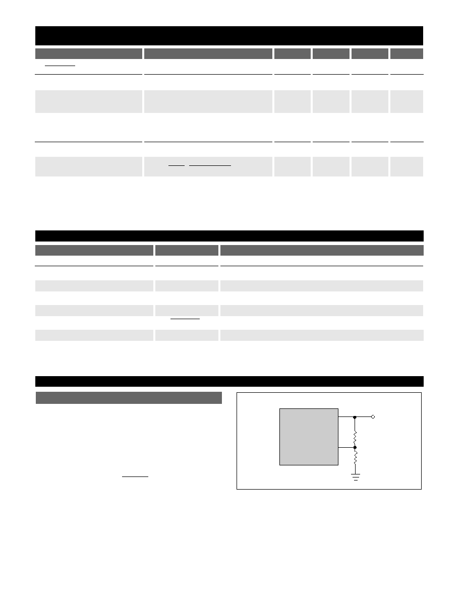
Package Pin Description
PACKAGE PIN #
PIN SYMBOL
FUNCTION
PARAMETER
TEST CONDITIONS
MIN
TYP
MAX
UNIT
Electrical Characteristics:
V
OUT
+ 1V ≤ V
IN
≤ 30V, 5V ≤ V
OUT
≤ 12V, I
OUT
= 10mA, -40° ≤ T
A
≤ 125°, -40° ≤ T
J
≤ 150°,
V
ENABLE
= 0V; unless otherwise specified.
The output voltage of the CS8271 is adjustable to any value
between the reference voltage on the Adj pin, (1.272V Typ.)
and the maximum input voltage minus the dropout voltage.
To adjust the output voltage, a pair of external resistors R1
and R2 are connected as shown in Figure 1.
The equation for the output voltage is
V
OUT
= V
REF
x
+ I
Adj
x R1
where V
ref
is the typical reference voltage and I
Adj
is the
adjust pin bias current. This is usually 500nA maximum.
Figure 1: Output Voltage Adjustment.
Adj
CS8271
V
OUT
R
1
V
OUT
R
2
V
REF
)
R1 + R2
R2
(
Output Voltage Adjustment
Circuit Description
8L SOIC & PDIP
1
V
OUT
100mA output; adjustable from 5V to 12V.
2
Gnd
Ground.
3, 6, 7
NC
No Connection.
4
Adj
Resistor divider from V
OUT
to Adj, sets output voltage.
5
Logic level switch, when HIGH, regulator is in sleep mode.
8
V
IN
Input voltage.
ENABLE
s
Enable Threshold
1.15
2.0
2.6
V
Enable Input Current
V
ENABLE
= 2.6V
10
20
µA
V
ENABLE
= 5V
35
50
µA
s Adjustment Pin
R1: Feedback resistor between V
OUT
and Adjust, R2: Adjust resistor to ground.
Reference Voltage
100µA ≤ I
OU T
≤ 100mA
1.246
1.272
1.297
V
Adjustment Pin Current
I
Adj
=
-
20
500
nA
Note 1: Guaranteed by design, not 100% tested in production.
(V
OUT
- V
REF
)
R1
V
REF
R2
ENABLE
4
CS8271
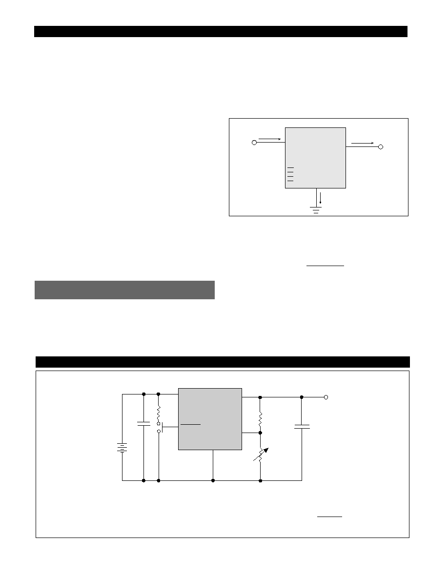
The output compensation capacitor C
OUT
, determines
three main characteristics of a linear regulator: start-up
delay, load transient response and loop stability.
The selection of a capacitor value and type should be
based on cost, availability, size and temperature con-
straints. A tantalum or aluminum electrolytic capacitor is
best, since a film or ceramic capacitor with almost zero
ESR, can cause instability. The aluminum electrolytic
capacitor is the least expensive solution, but, if the circuit
operates at low temperatures (-25°C to -40°C), both the
value and ESR of the capacitor will vary considerably. The
capacitor manufacturers data sheet usually provide this
information.
The value for the output compensation capacitor C
OUT
shown in Figure 3 should work for most applications, but it
is not necessarily the least expensive or the optimal solution.
Figure 3: Test and application circuit showing an output compensation
capacitor.
To determine an acceptable value for C
OUT
for a particular
application, start with a tantalum capacitor of the recom-
mended value and work towards a less expensive alterna-
tive part.
Step 1:
Place the completed circuit with a tantalum capac-
itor of the recommended value in an environmental cham-
ber at the lowest specified operating temperature. Monitor
the outputs on the oscilloscope. A decade box connected in
series with the capacitor will simulate the higher ESR of an
aluminum capacitor. (Leave the decade box outside the
chamber, the small resistance added by the longer leads is
negligible)
Step 2:
With the input voltage at its maximum value,
increase the load current slowly from zero to full load
while observing the output for any oscillations. If no oscil-
lations are observed, the capacitor is large enough to
ensure a stable design under steady state conditions.
Step 3:
Increase the ESR of the capacitor from zero using
the decade box and vary the load current until oscillations
appear. Record the values of load current and ESR that
cause the greatest oscillation. This represents the worst
case load conditions for the regulator at low temperature.
Step 4
: Maintain the worst case load conditions set in step
3 and vary the input voltage until the oscillations increase.
This point represents the worst case input voltage condi-
tions.
Step 5:
If the capacitor is adequate, repeat steps 3 and 4
with the next smaller valued capacitor. (A smaller capaci-
tor will usually cost less and occupy less board space.) If
the capacitor oscillates within the range of expected oper-
ating conditions, repeat steps 3 and 4 with the next larger
standard capacitor value.
Adj
CS8271
V
OUT
R
RST
C
OUT
10
mF
R
L
ENABLE
V
IN
C
IN
0.1
mF
C
Adj
(optional)
Selecting the Right Capacitor Value
Application Notes
The output stage is protected against overvoltage, short
circuit and thermal runaway conditions (Figure 2).
If the input voltage rises above 30V (e.g. load dump), the
output shuts down. This response protects the internal cir-
cuitry and enables the IC to survive unexpected voltage
transients up to 60V in magnitude.
Short circuit protection limits the amount of current the
output transistor can supply. In the case of a CS8271 under
a short circuit condition, the output transistor current is
limited to 100mA.
Figure 2: Typical Circuit Waveforms for Output Stage Protection.
Should the junction temperature of the power device exceed
180˚C (typ) the power transistor is turned off. Thermal shut-
down is an effective means to prevent die overheating since
the power transistor is the principle heat source in the IC.
The
switches the output transistor. When the
voltage on the
pin exceeds 2.0V typ, the output
pass transistor turns off, leaving a high impedance facing
the load. The IC will remain in Sleep mode, drawing only
20µA (typ), until the voltage on the
pin drops
below the
threshold.
ENABLE
ENABLE
ENABLE
ENABLE
ENABLE
I
OUT
V
OUT
V
IN
Load
Dump
Short
Circuit
Thermal
Shutdown
> 30V
Output Stage Protection
Circuit Description: continued
5
Application Diagram
CS8271
Adj
CS8271
V
OUT
R
2
R
1
C
2
**
10
mF
V
OUT
V
IN
Gnd
C
1
*
0.1
mF
V
ref
ENABLE
C
1
* Required if regulator is away from power supply filter.
C
2
** Required for output stability.
V
OUT
= V
ref
x
+ I
Adj
x R1
)
R1 + R2
R2
(
Step 6:
Test the load transient response by switching in
various loads at several frequencies to simulate its real
work environment. Vary the ESR to reduce ringing.
Step 7:
Remove the unit from the environmental chamber
and heat the IC with a heat gun. Vary the load current as
instructed in step 5 to test for any oscillations.
Once the minimum capacitor value with the maximum
ESR is found, a safety factor should be added to allow for
the tolerance of the capacitor and any variations in regula-
tor performance. Most good quality aluminum electrolytic
capacitors have a tolerance of ±20% so the minimum value
found should be increased by at least 50% to allow for this
tolerance plus the variation which will occur at low tem-
peratures. The ESR of the capacitor should be less than
50% of the maximum allowable ESR found in step 3 above.
Capacitance on the Adjust pin combined with the feed-
back resistors R1 and R2 can affect loop stability and
should also be considered. The CS8271 internal circuitry
produces about 5pF to Ground on the Adjust pin. This
capacitance, plus any additional external capacitance on
the Adjust pin will create a pole when combined with the
resistive feedback network. The effect can be significant
when using large values for the feedback resistors to mini-
mize quiescent current.
A capacitor connected from the Adjust pin to Ground pro-
vides additional means to compensate the regulator by
creating a pole. Alternately, a capacitor can be connected
from the Adjust pin to V
OUT
to create a zero.
The maximum power dissipation for a single output regu-
lator (Figure 4) is
P
D(max)
={V
IN(max)
–V
OUT(min)
}I
OUT(max)
+V
IN(max)
I
Q
(1)
where
V
IN(max)
is the maximum input voltage,
V
OUT(min)
is the minimum output voltage,
I
OUT(max)
is the maximum output current, for the applica-
tion
I
Q
is the quiescent current the regulator consumes at
I
OUT(max)
.
Figure 4: Single output regulator with key performance parameters
labeled.
Once the value of P
D(max)
is known, the maximum permis-
sible value of R
QJA
can be calculated:
R
QJA
=
(2)
The value of R
QJA
can then be compared with those in
the package section of the data sheet. Those packages with
R
QJA
's less than the calculated value in equation 2 will keep
the die temperature below 150°C.
In some cases, none of the packages will be sufficient to
dissipate the heat generated by the IC, and an external
heatsink will be required.
150°C - T
A
P
D
V
IN
Smart
Regulator
V
OUT
I
OUT
I
IN
I
Q
Control
Features
}
Calculating Power Dissipation
in a Single Output Linear Regulator
Application Notes: continued