 | –≠–ª–µ–∫—Ç—Ä–æ–Ω–Ω—ã–π –∫–æ–º–ø–æ–Ω–µ–Ω—Ç: CH7001 | –°–∫–∞—á–∞—Ç—å:  PDF PDF  ZIP ZIP |

CH7001C
201-0000-028 Rev 3.0, 6/2/99
1
CHRONTEL
VGA to NTSC/PAL Encoder
Features
∑ Enhanced bandwidth and signal-to-noise ratio for
higher video performance
∑ Integrated triple video rate 8-bit analog to digital
converters for input RGB
∑ 3-line digital vertical filtering with pin-
programmable characteristics for optimum anti-
flicker and resolution
∑ On-chip phase-locked loop generates sampling
clock from VGA horizontal sync
∑ Enhanced power management for selective circuit
power-down
∑ Simultaneous composite/S-video output
∑ Horizontal and vertical position control
∑ Pin-programmable underscan/overscan mode
∑ On-chip reference generation and loop filter
∑ CMOS technology in 44-pin PLCC
∑ 5V supply
Description
Chrontel's CH7001C VGA to NTSC/PAL encoder is a
stand-alone integrated circuit that converts analog VGA
inputs directly into 525-line (M) NTSC or 625-line
(B, D, G, H, I) PAL composite video and S-video
outputs.
This circuit integrates a digital NTSC/PAL encoder
with 8-bit ADC and DAC interfaces, a 3-line vertical
filter and low-jitter phase-locked loop to create
outstanding quality video with 24-bits-per-pixel proces-
sing throughout the entire signal path.
A high level of integration and performance makes the
CH7001C ideal for a variety of stand-alone and system-
level integration solutions, including notebook
computers and PC add-on graphics cards.
Figure 1: Functional Block Diagram
ADC
ADC
ADC
VERTICAL
SCAN-RATE
COLOR
SPACE
CONVERTER
CONVERTER
FILTER
U
FILTER
V
FILTER
DAC
DAC
DAC
X
M
U
X
M
U
X
M
U
X
Y
FILTER
BLANKING COLOR-BURST
CONTROL
BLANKING
H,V SYNC
GENERATOR
X
SIN + COSINE
GENERATOR
PLL
OSC
SYSTEM CLOCKS
R
G
B
H
V
Y
CVBS
C
MS[1:0]
RSET
RSET
AVDD
VDD
VREF
VREF1
VREF2
UNDERSCAN
PD[1:0]
NTSC/PAL*
CLKEN*
HORIZONTAL, VERTICAL
POSITION CONTROL
STROBE
CLKOUT
DVDD
CHRONTEL
CH7001C
2
201-0000-028 Rev 3.0, 6/2/99
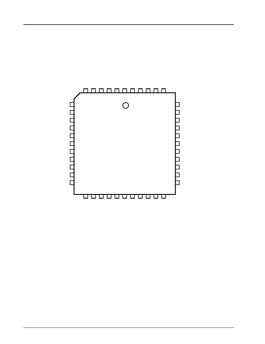
Figure 2: 44-pin PLCC
VREF2
AVDD
TEST*
H
CLKEN*
CLKOUT
DVDD
DVDD
DGND
MS0
MS1
V
UNDERSCAN
DVDD
DGND
XI
XO/FIN
PDI
PD0
DGND
NTSC/PAL*
RIGHT
S
T
R
O
B
E
A
G
N
D
A
V
D
D
G
A
G
N
D
B
A
V
D
D
R
A
G
N
D
V
R
E
F
1
A
G
N
D
V
D
D
R
S
E
T
G
N
D
G
N
D
Y
C
V
B
S
C
V
D
D
U
P
D
O
W
N
L
E
F
T
7
8
9
10
13
12
11
39
38
37
36
35
14
15
16
17
34
33
32
31
30
29
6
5
4
3
2
1
4
4
4
3
4
2
4
1
4
0
1
8
1
9
2
0
2
1
2
4
2
3
2
2
2
5
2
6
2
7
2
8
CHRONTEL
CH7001C

CHRONTEL
CH7001C
201-0000-028 Rev 3.0, 6/2/99
3
Note:
1 The Typical Connection Diagram (Figure 4 on page 6) shows the VGA input configured for applications that do not require
RGB buffering before the monitor. In this configuration, 75
input termination must be guaranteed either by termination by the
monitor connection, by discrete 75
resistors on the PCB, or by a dummy 75
termination connector. The total RGB trace on
the PCB must be kept as short as possible to avoid cable reflection problems. For further information, request a copy of
Application Note AN-11, "PC Board Layout Considerations for CH7001C. "
2 Please refer to crystal manufacturer specifications for proper load capacitances. The optional variable tuning capacitor is
required only if the crystal oscillation frequency cannot be controlled to the required accuracy. The capacitance value for the
tuning capacitor should be obtained from the crystal manufacturer. For further information, request a copy of Application Note
AN-19, "Tuning Clock Outputs. "
Table 1 ∑ Pin Description
Pin
Type
Symbol
Description
1, 5, 40, 42
Power
AGND
Analog ground
These pins provide the ground reference for the analog section of
CH7001C, and MUST be connected to the system ground to
prevent latchup. Please refer to Application Note AN-11 for
information on proper supply decoupling.
2, 4, 44
In
G, R, B
VGA Inputs
1
These pins should be terminated with 75
resistors and isolated
from switching digital signals and video output pins.
3, 38, 43
Power
AVDD
Analog Supply Voltage
These pins supply the 5V power to the analog section of the
CH7001C. For information on proper supply decoupling, please
refer to Application Note AN-11.
6
In
STROBE
Strobe Input (active high, internal pull-up)
A logical HIGH input to this pin keeps chip mode pins (CLKEN*,
UNDERSCAN, MS[1:0], UP, DOWN, LEFT, and RIGHT) active.
These input signals are internally sampled on the high-to-low
transition of the STROBE signal. This allows the chip state to be
maintained while rendering these mode pins inactive.
7
In
CLKEN*
Clock Enable (active low, internal pull-up)
A logical LOW input to this pin enables CLKOUT. CLKEN* should
be hardwired to ground to enable CLKOUT. Otherwise, CLKEN*
should be left unconnected or connected to VDD.
8
Out
CLKOUT
Clock Output
This pin defaults to 14.31818 MHz upon power-up. Further toggling
of the CLKEN* pin causes CLKOUT to output other internal test
clocks. When disabled (i.e., CLKEN*=1), this output is a logic LOW.
Setting the PD* pin low also causes CLKOUT to be logic LOW.
9, 13, 32
Power
DVDD
Digital Supply Voltage
These pins supply the 5V power to the digital section of CH7001C.
For information on proper supply decoupling, please refer to
Application Note AN-11.
10, 14, 31
Power
DGND
Digital Ground
These pins provide the ground reference for the digital section of
CH7001C, and MUST be connected to the system ground to
prevent latchup. For information on proper supply decoupling,
please refer to Application Note AN-11.
11, 12
In
MS0, MS1
Anti-flicker Mode Select Pins
These two pins are used to select one of four possible anti-flicker
vertical filter modes.
15
In
XI
Crystal Input
2
A 14.31818 MHz parallel resonance (±
50 ppm) crystal should be
attached between XI and XO/FIN. However, if an external CMOS
clock is attached to XO/FIN, XI should be connected to ground.
16
In
XO/FIN
Crystal Output or External F
REF
Input
2
A 14.31818 MHz (±
50 ppm) crystal may be attached between
XO/FIN and XI. An external CMOS compatible clock can be
connected to XO/FIN as an alternative.

CHRONTEL
CH7001C
4
201-0000-028 Rev 3.0, 6/2/99
Table 1 ∑ Pin Description (continued)
Pin
Type
Symbol
Description
17, 37
In
PDI, PD0
Power Down Inputs (active low, internal pull-up)
Asserting these signals place CH7001C into different power-down
states. (Refer to section on Power Management). Note: Use of
these pins is optional. Leaving these two pins floating will maintain
normal operating mode.
18, 25
Power
VDD
DAC Power Supply
These pins supply power to CH7001C's internal DACs. Please refer
to Application Note AN-11 for information on proper supply
decoupling.
19
In
RSET
Reference Resistor
A 330
resistor with short and wide traces should be attached
between RSET and ground. No other connections should be made
to this pin.
20, 24
Power
GND
DAC Ground
These pins provide the ground reference for CH7001C's internal
DACs. For information on proper supply decoupling, please refer to
Application Note AN-11.
21
Out
Y
Luminance Output
A 75
termination resistor with short traces should be attached
between Y and ground for optimum performance. An optional low
pass filter circuit, shown in Figure 3 on page 5, may be used as an
alternative to the ferrite bead shown in Figure 4 on page 6.
22
Out
CVBS
Composite Output
A 75
termination resistor with short traces should be attached
between CVBS and ground for optimum performance. An optional
low pass filter circuit shown in Figure 3 on page 5, may be used as
an alternative to the ferrite bead shown in Figure 4 on page 6.
23
Out
C
Chrominance Output
A 75
termination resistor with short traces should be attached
between C and ground for optimum performance. An optional low
pass filter circuit shown in Figure 3 on page 5, may be used as an
alternative to the ferrite bead shown on Figure 4 on page 6.
26
In
UP
Up Position Control (active low, internal pull-up)
UP allows the screen display position to be moved up incrementally
for every toggle of this pin to ground. An internal schmitt trigger
minimizes switch bounce problems. UP may be connected directly
to the power supply or ground.
27
In
DOWN
Down Position Control (active low, internal pull-up)
DOWN allows the screen display position to be moved down
incrementally for every toggle of this pin to ground. An internal
schmitt trigger minimizes switch bounce problems. DOWN may be
connected directly to the power supply or ground.
28
In
LEFT
Left Position Control (active low, internal pull-up)
LEFT allows the screen display position to be moved to the left
incrementally for every toggle of this pin to ground. An internal
schmitt trigger minimizes switch bounce problems. LEFT may be
connected directly to the power supply or ground.
29
In
RIGHT
Right Position Control (active low, internal pull-up)
RIGHT allows the screen display position to be moved to the right
incrementally for every toggle of this pin to ground. An internal
schmitt trigger minimizes switch bounce problems. RIGHT may be
connected directly to the power supply or ground.
30
In
NTSC / PAL*
NTSC/PAL Mode Select Input (internal pull-up)
A logical HIGH input NTSC/PAL* pin selects NTSC operation. A
logical LOW input to NTSC/PAL* selects PAL operation. NTSC/PAL*
accepts CMOS logic level inputs and may be connected directly to
the power supply or ground.

CHRONTEL
CH7001C
201-0000-028 Rev 3.0, 6/2/99
5
Table 1
∑
Pin Description (continued)
Figure 3: Optional Output Filter
Pin
Type
Symbol
Description
33
In
UNDERSCAN
Underscan Enable Pin (active high, internal pull-up)
A logical HIGH input to UNDERSCAN results to an output screen
that has approximately 12.5% horizontal underscan. This pin may
be connected directly to the power supply or ground.
34
In
V
Vertical Sync Input
This pin accepts the vertical sync output from the VGA card. The
capacitive loading on this pin should kept to a minimum.
35
In
H
Horizontal Sync Input
This pin accepts the horizontal sync output from the VGA card. The
capacitive loading on this pin should kept to a minimum. Please
refer to Application Note 11 "PC Board Layout Considerations
for CH7001C."
36
--
TEST*
Test Pin (active low, internal pull-up)
Connect a capacitor in the range of 2.2uF - 4.7uF from this pin
to GND to ensure proper functionality of the UNDERSCAN/
OVERSCAN feature.
39
In
VREF2
Internal Voltage Reference
VREF2 provides a typical 2.5V reference that is used as an internal
bias to the ADCs. A 0.1
µ
F decoupling capacitor should be
connected between VREF2 and ground.
41
In
VREF1
ADC Voltage Reference Input / Output
VREF1 provides a typical 1.235V reference that sets the RGB input
full scale at 0.75V. A 0.1
µ
F decoupling capacitor should be
connected between VREF1 and ground. VREF1 may also be forced
by external reference.
1
Optional Output Filter
Y,C, CVBS
75 Ohms
150pF
270pF
1.2uH
47pF
1.2uH
OUTPUT