 | –≠–ª–µ–∫—Ç—Ä–æ–Ω–Ω—ã–π –∫–æ–º–ø–æ–Ω–µ–Ω—Ç: CH7205A-D | –°–∫–∞—á–∞—Ç—å:  PDF PDF  ZIP ZIP |

CH7205A
Brief Datasheet
209-0000-022
Rev. 1.41, 2/19/2003
1
Chrontel
CH7205 DVD-TV Encoder
1.0 F
EATURES
2.0
G
ENERAL
D
ESCRIPTION
∑ YPrPb support for 480i, 576i, 480p and 576p Output
∑ Macrovision
TM
7.1.L1 copy protection support
∑ Programmable digital input interface supporting RGB
and YCrCb input data formats
∑ Interlaced to progressive scan conversion for DVD
∑ Support for NTSC, PAL TV and Progressive Scan
formats
∑ Support for SCART output
∑ TV connection detection
∑ Outputs of CVBS, S-Video and YPbPr
∑ Two sets of individual DAC output pins, CVBS, S-
Video and YPbPr to allow switching among TV- out
connectors without additional external video switches
∑ Programmable power management
∑ Four 10-bit video DAC outputs
∑ Fully programmable through serial port
∑ Offered in a 48-pin LQFP package
The CH7205 is a video TV encoder device for DVD
application which accepts a digital video input signal, encodes
and transmits data through four 10-bit high speed DACs. The
device is able to generate synchronization signals for NTSC
and PAL TV standards with CVBS, S-Video outputs, and
YPrPb interface 480i, 576i, 480p and 576p consumer video
outputs.
The device accepts data over one 12-bit (or 8-bit) wide data
port with dual edge clock data transfer for multiplexed data
(24 bit or 16 bit) through variable voltage data port which
supports 5 different data formats including RGB and YCrCb.
A high accuracy low jitter phase locked loop is integrated to
create outstanding video quality. Support is provided for
Macrovision
TM
. ITU-R BT.656 interlaced video can be input
and scan converted to non-interlaced video.
Figure 1: Functional Block Diagram (CH7205 48 pin package)
XCLK,XCLK*
Serial
Port
Control
D[11:0]
H,V
Data
Latch,
Demux
2
12
H,V
Latch
Clock
Driver
VREF
XI/FIN,XO
P-OUT
BCO/V-Sync
PLL
Timing
Color Space
Conversion
Sync Decode
NTSC/PAL
Encode,
480i/576i
480p/576p
YPrPb
MUX
RGB
YPbPr
2
2
Four
10-bit DAC's
DAC 3
DAC 2
DAC 1
DAC 0
Video
Switch
Serial Data
GPIO[1:0]
RESET*
ISET
DACA[3:0]
DACB[3:1]
Serial Clcok
CVBS, S-Video,
2
4
3
CHRONTEL
CH7205A
2 209-0000-022
Rev. 1.41, 2/19/2003
3.0
P
IN
-O
UT
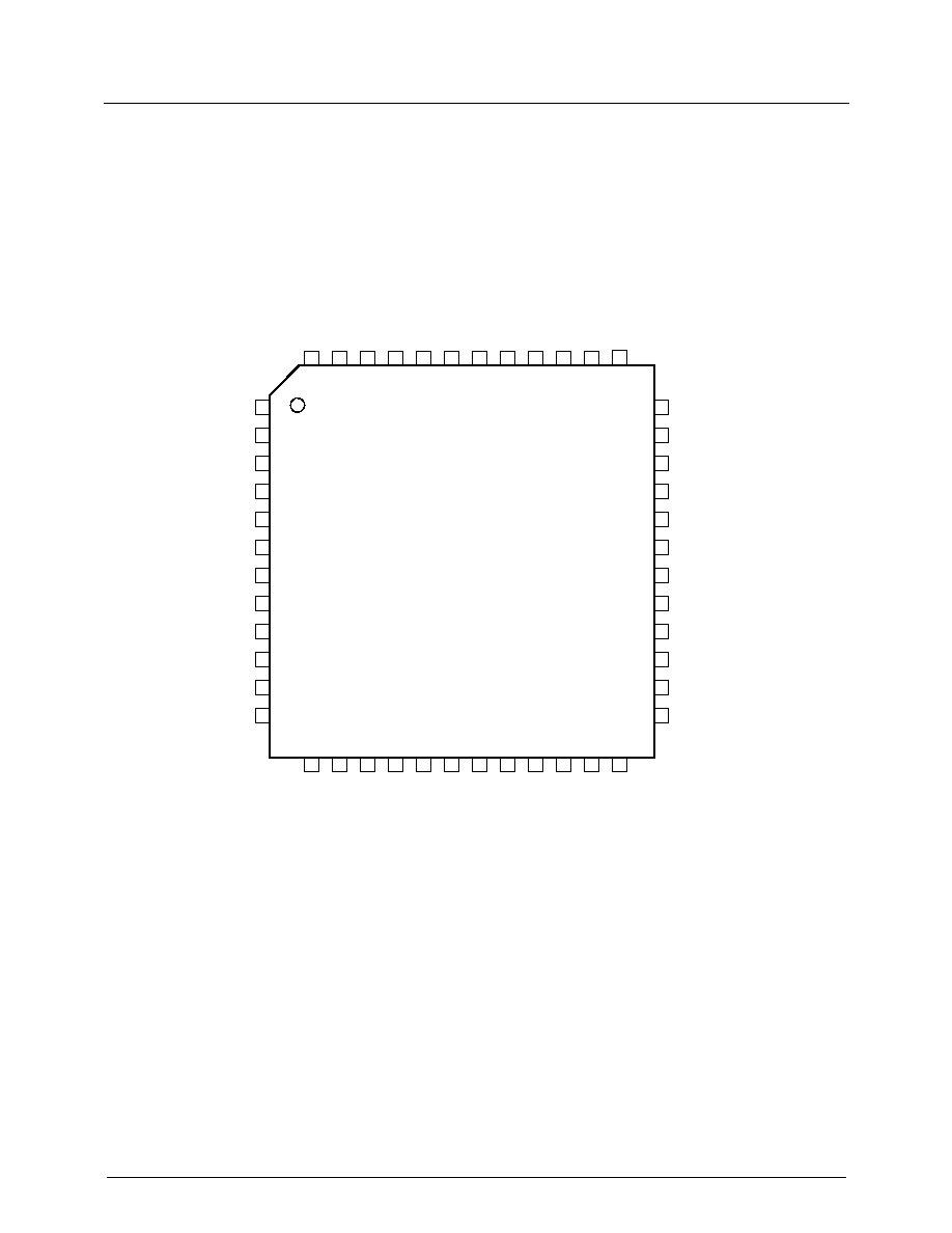
3.1 Package
Diagram
D[3]
D[4]
D[5]
D[6]
DVDD
D[7]
D[8]
DGND
D[9]
D
[
11]
XO
XI/FIN
AVDD
DVDD
RESET*
DGND
SPC
SPD
VDD
ISET
GND
DGND
XC
LK*
GPIO[0]
VR
EF
DV
DD
C
VBS
GND
C
VBS/B
C/R
Y/G
D[2]
D[1]
D[0
]
V
H
XC
LK
V
DDV
P-
Out
DGND
BC
O/VSYN
C
AGN
D
18
43
44
45
46
47
48
41
42
39
40
38
17
16
15
14
13
19
22
21
20
23
36
35
34
33
32
31
30
29
28
27
26
1
2
3
4
5
6
7
8
9
10
11
CHRONTEL
CH7205
12
D[10]
Pb/B
Pr
/R
24
GPIO[1]/CHSYNC
Y/G
25
37
N/C
Figure 2: 48-Pin LQFP Package
CHRONTEL
CH7205A
209-0000-022
Rev. 1.41, 2/19/2003
3
3.2 Pin
Description
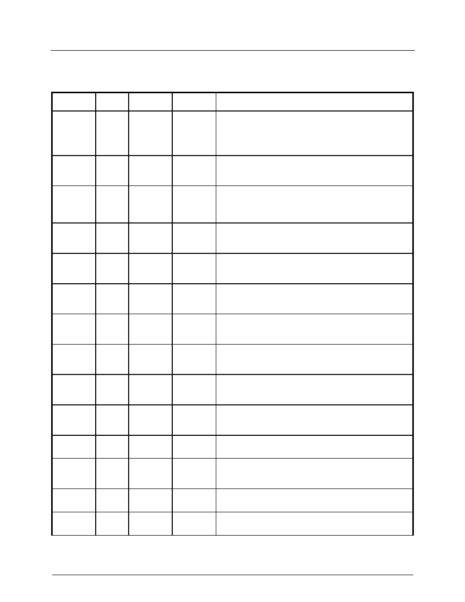
Table 1: Pin Description
Pin #
# of
Pins
Type Symbol
Description
1-4,
6,7,
9-13,
48
12 In
D[11]-D[0]
Data[11] through Data[0] Inputs
These pins accept the 12 data inputs from a digital video port The levels are
0 to DVDDV, and the VREF signal is used as the threshold level.
14 1
In/Out
GPIO0
General Purpose Input ≠ Output0 (weak internal pull-up)
This pin provides general purpose I/O controlled via the serial port. This
allows an external switch to be used to select NTSC or PAL at power-up. The
internal pull-up will be to the DVDD supply.
15 1
In/Out
GPIO1
/
CSYNC
General Purpose Input ≠ Output1 (weak internal pull-up)
This pin provides general purpose I/O controlled via the serial port. This
allows an external switch to be used to select NTSC or PAL at power-up. The
internal pull-up will be to the DVDD supply. It can also be configured to
output composite sync.
17 1
Out CVBS
(DACA0)
Composite Video
This pin outputs a composite video signal capable of driving a 75 ohm doubly
terminated load. During bypass modes this output is valid only if the data
format is compatible with one of the TV-Out display modes.
20 1
Out Pb/Cb
(DACB3)
Pb / Cb Output
This pin outputs a selectable video signal. The output is designed to drive a
75 ohm doubly terminated load. The output can be selected to the Pb
component of YPrPb or the Cb component of YCrCb.
21 1
Out CVBS/B
(DACA3)
Composite Video / Blue Output
This pin outputs a selectable video signal. The output is designed to drive a
75 ohm doubly terminated load. The output can be selected to be composite
video or blue (for SCART type 1 connections).
22 1
Out Pr/Cr
(DACB2)
Pr / Cr Output
This pin outputs a selectable video signal. The output is designed to drive a 75
ohm doubly terminated load. The output can be selected to be the Pr
component of YPrPb or the Cr component of YCrCb.
23 1
Out C/R
(DACA2)
Chroma / Red Output
This pin outputs a selectable video signal. The output is designed to drive a 75
ohm doubly terminated load. The output can be selected to be s-video
chrominance or red (for SCART type 1 connections).
24 1
Out Y
(DACB1)
Luma
This pin outputs a selectable video signal. The output is designed to drive a 75
ohm doubly terminated load. The output can be selected to be s-video
luminance.
25 1
Out Y/G
(DACA1)
Luma / Green Output
This pin outputs a selectable video signal. The output is designed to drive a 75
ohm doubly terminated load. The output can be selected to be the luminance
component of YPrPb.
27 1
In ISET
Current Set Resistor Input
This pin sets the DAC current. A 140 ohm resistor should be connected
between this pin and GND (pin 26) using short and wide traces.
29 1
In/Out
SPD
Serial Port Data Input / Output
This pin functions as the bi-directional data pin of the serial port and operates
with inputs from 0 to VDDV. Outputs are driven from 0 to VDDV. The serial
port address is 76h.
30 1
In SPC
Serial Port Clock Input
This pin functions as the clock pin of the serial port, and uses the DVDD
supply.
32 1
In RESET*
Reset * Input (Internal pull-up)
When this pin is low, the device is held in the power-on reset condition.
When this pin is high, reset is controlled through the serial port.

CHRONTEL
CH7205A
4 209-0000-022
Rev. 1.41, 2/19/2003
Table 1: Pin Description (continued)
Pin #
# of
Pins
Type Symbol
Description
35
1
In
XI / FIN
Crystal Input / External Reference Input
A parallel resonance 14.31818MHz crystal (+ 20 ppm) should be attached
between this pin and XO. However, an external CMOS compatible clock can
drive the XI/FIN input.
36 1
Out XO Crystal Output
A parallel resonance 14.31818MHz crystal (+ 20 ppm) should be attached
between this pin and XI / FIN. However, if an external CMOS clock is
attached to XI/FIN, XO should be left open.
38 1
Out BCO/
VSYNC
Buffered Clock Output / VSYNC
This output pin provides selectable buffered clocks to be output, driven by the
DVDD supply. The output clock can be selected using the BCO register. The
levels are 0 to DVDD. This pin can output VSYNC in bypass RGB mode.
40 1
Out P-OUT
Pixel Clock Output
This pin provides a pixel clock signal to the controller which can be used as a
reference frequency. The output is selectable between 1X and 2X of the pixel
clock frequency. The output driver is driven from the DVDDV supply. This
output has a programmable tri-state. The capacitive loading on this pin should
be kept to a minimum.
42 1
In VREF
Reference Voltage Input
The VREF pin inputs a reference voltage of DVDDV / 2. The signal is
derived externally through a resistor divider and decoupling capacitor, and
will be used as a reference level for data, sync and clock inputs.
43, 44
2
In
XCLK,
XCLK*
External Clock Inputs
These inputs form a differential clock signal input to the device for use with
the H, V and D[11:0] data. If differential clocks are not available, the XCLK*
input should be connected to VREF.
The clock polarity used can be selected by the MCP control bit.
45 1
In/Out
H Horizontal Sync Input / Output
When the SYO control bit is low, this pin accepts a horizontal sync input for
use with the input data. The amplitude will be 0 to DVDDV, and the VREF
signal is used as the threshold level. This pin must be used as an input in all
bypass modes.
When the SYO control bit is high, the device will output a horizontal sync
pulse, 64 pixels wide. The output is driven from the DVDD supply. This
output is valid with TV-Out operation.
46 1
In/Out
V Vertical Sync Input / Output
When the SYO control bit is low, this pin accepts a vertical sync input for use
with the input data. The amplitude will be 0 to DVDDV, and the VREF
signal is used as the threshold level. This pin must be used as an input in all
bypass modes.
When the SYO control bit is high, the device will output a vertical sync pulse
one line wide. The output is driven from the DVDD supply. This output is
valid with TV-Out operation.
5,16,33 3 Power DVDD Digital Supply Voltage (3.3V)
8,18,31,39 4
Power
DGND
Digital Ground
41 1
Power
VDDV
I/O Supply Voltage (1.1V to 3.3V)
34 1
Power
AVDD
PLL Supply Voltage (3.3V)
37 1
Power
AGND
PLL Ground
28 1
Power
VDD
DAC Supply Voltage (3.3V)
19,26 2 Power GND DAC Ground

CHRONTEL
CH7205A
209-0000-022
Rev. 1.41, 2/19/2003
5
4.0
P
ACKAGE
D
IMENSIONS
Figure 3: 48 Pin LQFP Package
Table of Dimensions
No. of Leads
SYMBOL
48 (7 X 7 mm)
A
B
C
D
E
F
G
H
I
J
MIN 0.17
1.35
0.05
0.45
0.09
0
∞
∞
∞
∞
Milli-
meters
MAX
9 7 0.5
0.27 1.45 0.15
1.00
0.75 0.20 7
∞
∞
∞
∞