 | –≠–ª–µ–∫—Ç—Ä–æ–Ω–Ω—ã–π –∫–æ–º–ø–æ–Ω–µ–Ω—Ç: CDB4382 | –°–∫–∞—á–∞—Ç—å:  PDF PDF  ZIP ZIP |

Copyright
©
Cirrus Logic, Inc. 2004
(All Rights Reserved)
http://www.cirrus.com
CS4382
114 dB, 192 kHz 8-Channel D/A Converter
Features
24-bit Conversion
Up to 192 kHz Sample Rates
114 dB Dynamic Range
-100 dB THD+N
Supports PCM and DSD Data Formats
Selectable Digital Filters
Volume Control with Soft Ramp
≠ 1 dB Step Size
≠ Zero Crossing Click-free Transitions
Dedicated DSD inputs
Low Clock Jitter Sensitivity
Simultaneous Support for Two Synchronous
Sample Rates for DVD Audio
µ
C or Stand-alone Operation
Description
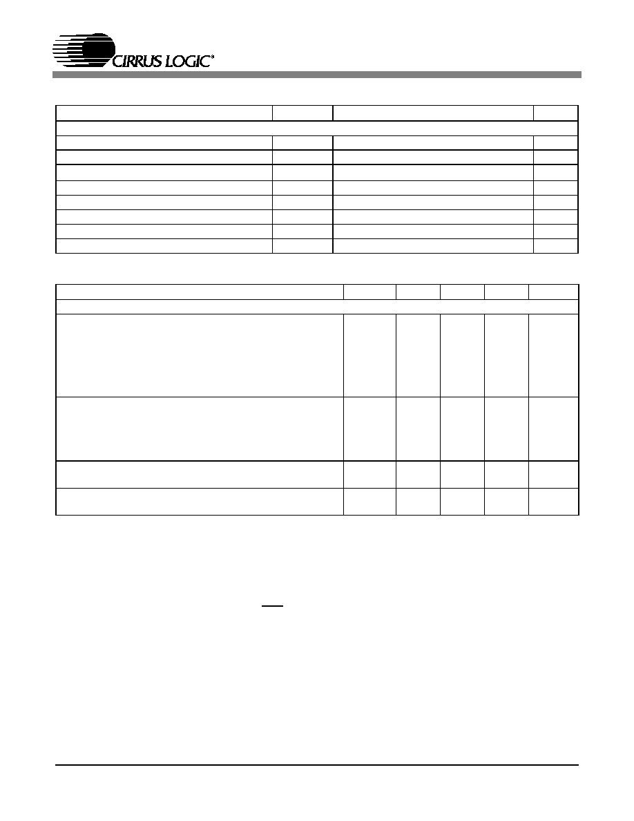
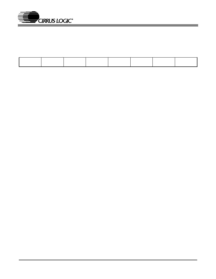
The CS4382 is a complete 8-channel digital-to-analog
system including digital interpolation, fifth-order delta-
sigma digital-to-analog conversion, digital de-emphasis,
volume control and analog filtering. The advantages of
this architecture include: ideal differential linearity, no
distortion mechanisms due to resistor matching errors,
no linearity drift over time and temperature and a high
tolerance to clock jitter.
The CS4382 accepts PCM data at sample rates from
4 kHz to 192 kHz, DSD audio data, and operates over a
wide power supply range. These features are ideal for
multi-channel audio systems including DVD players,
SACD players, A/V receivers, digital TV's, mixing con-
soles, effects processors, and automotive audio
systems.
ORDERING INFORMATION
CS4382-KQZ, Lead Free -10 to 70 ∞C
48-pin LQFP
CDB4382
Evaluation Board
I
E x t e r n a l
M u t e C o n t r o l
R S T
V o l u m e C o n t r o l
I n t e r p o l a t i o n F i lt e r
A n a l o g F i l t e r
D A C
M i x e r
V o l u m e C o n t r o l
D A C
A n a l o g F i l t e r
I n t e r p o l a t i o n F i lt e r
V o l u m e C o n t r o l
I n t e r p o l a t i o n F i lt e r
A n a l o g F i l t e r
D A C
M i x e r
V o l u m e C o n t r o l
D A C
A n a l o g F i l t e r
I n t e r p o l a t i o n F i lt e r
V o l u m e C o n t r o l
I n t e r p o l a t i o n F i lt e r
A n a l o g F i l t e r
D A C
M i x e r
V o l u m e C o n t r o l
D A C
A n a l o g F i l t e r
A O U T B 4 -
I n t e r p o l a t i o n F i lt e r
M C L K
Se
r
i
a
l
P
o
r
t
S C L /C C L K (M 1 )
S D A /C D IN (M 2 )
A D 0 /C S (M 0 ) V L C
˜
2
V Q
F IL T +
V A
G N D
V D
M U T E C 1
D S D _ S C L K (M 3 )
G N D
C o n tro l P o rt(S ta n d -A lo n e M o d e S e le c t)
V L S
L R C K
S D I N 1
S D I N 2
S D I N 3
2
S C L K
L R C K 2
S C L K
D S D x x
8
A O U T B 4 +
A O U T A 4 -
A O U T A 4 +
A O U T B 2 -
A O U T B 2 +
A O U T A 2 -
A O U T A 2 +
A O U T B 1 -
A O U T B 1 +
A O U T A 1 -
A O U T A 1 +
V o l u m e C o n t r o l
I n t e r p o l a t i o n F i lt e r
A n a l o g F i l t e r
D A C
M i x e r
V o l u m e C o n t r o l
D A C
A n a l o g F i l t e r
I n t e r p o l a t i o n F i lt e r
A O U T B 3 -
A O U T B 3 +
A O U T A 3 -
A O U T A 3 +
S D I N 4
M U T E C 2 3 4
1
1
NOV `04
DS514F1

CS4382
2
DS514F1
TABLE OF CONTENTS
1. CHARACTERISTICS AND SPECIFICATIONS ........................................................................ 4
ANALOG CHARACTERISTICS ................................................................................................ 4
POWER AND THERMAL CHARACTERISTICS....................................................................... 5
ANALOG FILTER RESPONSE................................................................................................. 6
DIGITAL CHARACTERISTICS ................................................................................................. 7
ABSOLUTE MAXIMUM RATINGS ........................................................................................... 7
RECOMMENDED OPERATING CONDITIONS ....................................................................... 7
SWITCHING CHARACTERISTICS .......................................................................................... 8
DSD - SWITCHING CHARACTERISTICS................................................................................ 9
SWITCHING CHARACTERISTICS - CONTROL PORT - I
2
C FORMAT ................................ 10
SWITCHING CHARACTERISTICS - CONTROL PORT - SPITM FORMAT............................ 11
2. REGISTER QUICK REFERENCE .......................................................................................... 14
3. REGISTER DESCRIPTION .................................................................................................... 15
4. PIN DESCRIPTION ................................................................................................................. 24
5. APPLICATIONS ...................................................................................................................... 27
5.1 Grounding and Power Supply Decoupling ....................................................................... 27
5.2 Oversampling Modes ....................................................................................................... 27
5.3 Recommended Power-up Sequence ............................................................................... 27
5.4 Analog Output and Filtering ............................................................................................. 27
5.5 Interpolation Filter ............................................................................................................ 27
5.6 Clock Source Selection .................................................................................................... 28
5.7 Using DSD mode ............................................................................................................. 28
6. CONTROL PORT INTERFACE .............................................................................................. 29
6.1 Enabling the Control Port ................................................................................................. 29
6.2 Format Selection .............................................................................................................. 29
6.3 I
2
C Format ....................................................................................................................... 29
6.3.1 Writing in I
2
C Format ........................................................................................... 29
6.3.2 Reading in I
2
C Format ........................................................................................ 29
6.4 SPI Format ....................................................................................................................... 30
6.4.1 Writing in SPI ...................................................................................................... 30
6.5 Memory Address Pointer (MAP) ................................................................................. 31
7. PARAMETER DEFINITIONS .................................................................................................. 39
8. REFERENCES ........................................................................................................................ 40
9. PACKAGE DIMENSIONS ....................................................................................................... 41
LIST OF FIGURES
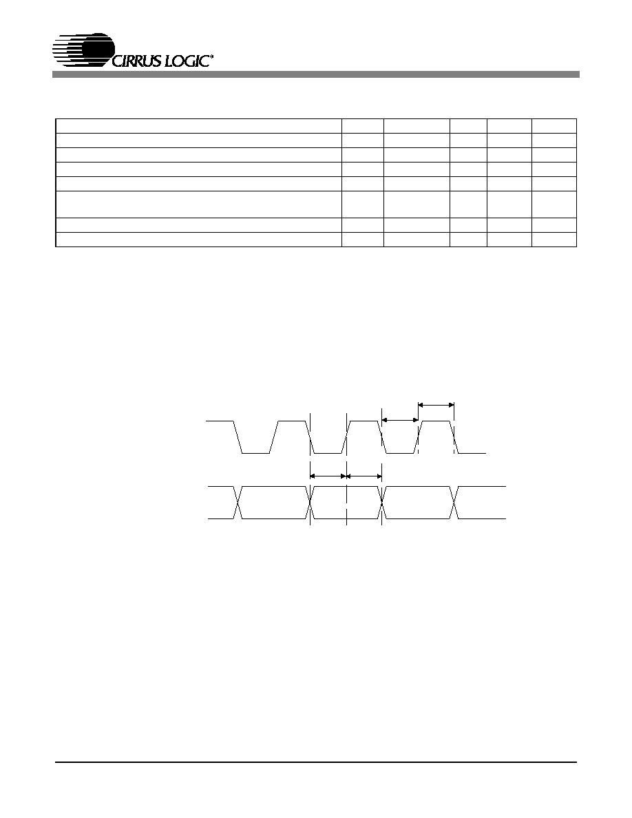
Figure 1. Serial Mode Input Timing ................................................................................................. 8
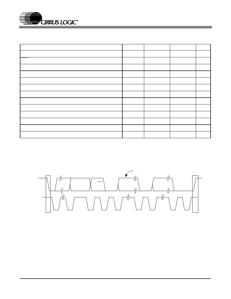
Figure 2. Direct Stream Digital - Serial Audio Input Timing............................................................. 9
Figure 3. Control Port Timing - I
2
C Format ................................................................................... 10
Figure 4. Control Port Timing - SPI Format................................................................................... 11
Figure 5. Typical Connection Diagram Control Port...................................................................... 12
Figure 6. Typical Connection Diagram Stand-Alone ..................................................................... 13
Figure 7. Control Port Timing, I
2
C Format..................................................................................... 30
Figure 8. Control Port Timing, SPI Format .................................................................................... 30
Figure 9. Single Speed (fast) Stopband Rejection ........................................................................ 32
Figure 10. Single Speed (fast) Transition Band ............................................................................ 32
Figure 11. Single Speed (fast) Transition Band (detail) ................................................................ 32
Figure 12. Single Speed (fast) Passband Ripple .......................................................................... 32
Figure 13. Single Speed (slow) Stopband Rejection..................................................................... 32
Figure 14. Single Speed (slow) Transition Band ........................................................................... 32
Figure 15. Single Speed (slow) Transition Band (detail) ............................................................... 33
Figure 16. Single Speed (slow) Passband Ripple ......................................................................... 33

CS4382
DS514F1
3
Figure 17. Double Speed (fast) Stopband Rejection..................................................................... 33
Figure 18. Double Speed (fast) Transition Band........................................................................... 33
Figure 19. Double Speed (fast) Transition Band (detail)............................................................... 33
Figure 20. Double Speed (fast) Passband Ripple......................................................................... 33
Figure 21. Double Speed (slow) Stopband Rejection ................................................................... 34
Figure 22. Double Speed (slow) Transition Band ......................................................................... 34
Figure 23. Double Speed (slow) Transition Band (detail) ............................................................. 34
Figure 24. Double Speed (slow) Passband Ripple ....................................................................... 34
Figure 25. Quad Speed (fast) Stopband Rejection ....................................................................... 34
Figure 26. Quad Speed (fast) Transition Band ............................................................................. 34
Figure 27. Quad Speed (fast) Transition Band (detail) ................................................................. 35
Figure 28. Quad Speed (fast) Passband Ripple ........................................................................... 35
Figure 29. Quad Speed (slow) Stopband Rejection...................................................................... 35
Figure 30. Quad Speed (slow) Transition Band ............................................................................ 35
Figure 31. Quad Speed (slow) Transition Band (detail) ................................................................ 35
Figure 32. Quad Speed (slow) Passband Ripple .......................................................................... 35
Figure 33. Format 0 - Left Justified up to 24-bit Data.................................................................... 36
Figure 34. Format 1 - I
2
S up to 24-bit Data................................................................................... 36
Figure 35. Format 2 - Right Justified 16-bit Data .......................................................................... 36
Figure 36. Format 3 - Right Justified 24-bit Data .......................................................................... 36
Figure 37. Format 4 - Right Justified 20-bit Data .......................................................................... 37
Figure 38. Format 5 - Right Justified 18-bit Data .......................................................................... 37
Figure 39. De-Emphasis Curve..................................................................................................... 37
Figure 40. Channel Pair Routing Diagram (x = Channel Pair 1, 2, 3, or 4)................................... 37
Figure 41. ATAPI Block Diagram (x = channel pair 1, 2, 3, or 4) .................................................. 38
Figure 42. Recommended Output Filter........................................................................................ 38
LIST OF TABLES
Table 1. Digital Interface Formats - PCM Mode............................................................................ 16
Table 2. Digital Interface Formats - DSD Mode ............................................................................ 16
Table 3. ATAPI Decode ................................................................................................................ 21
Table 4. Example Digital Volume Settings .................................................................................... 22
Table 5. Common Clock Frequencies........................................................................................... 26
Table 6. Digital Interface Format, Stand-Alone Mode Options...................................................... 26
Table 7. Mode Selection, Stand-Alone Mode Options .................................................................. 26
Table 8. Direct Stream Digital (DSD), Stand-Alone Mode Options ............................................... 26
Table 9. Revision History ............................................................................................................. 42

CS4382
4
DS514F1
1.
CHARACTERISTICS AND SPECIFICATIONS
ANALOG CHARACTERISTICS
(Full-Scale Output Sine Wave, 997 Hz; Measurement Bandwidth
10 Hz to 20 kHz, unless otherwise specified; Test load R
L
= 3 k
, C
L
= 100 pF
,
VA = 5 V, VD = 3.3 V (see Figure 5)
For Single speed Mode Fs = 48 kHz, SCLK = 3.072 MHz, MCLK = 12.288 MHz;
For Double Speed Mode Fs = 96 kHz, SCLK = 6.144 MHz, MCLK = 12.288 MHz;
For Quad Speed Mode Fs = 192 kHz, SCLK = 12.288 MHz, MCLK = 24.576 MHz;
For Direct Stream Digital Mode Fs = 128 x 48 kHz, DSD_SCLK = 6.144 MHz, MCLK = 12.288 MHz).
Notes: 1. CS4382-KQZ parts are tested at 25 ∞C.
2. One-half LSB of triangular PDF dither is added to data.
3. Performance limited by 16-bit quantization noise.
Parameters
Symbol
Min
Typ
Max
Unit
CS4382-KQZ Dynamic Performance - All PCM modes and DSD (Note 1)
Specified Temperature Range
T
A
-10
-
70
∞C
Dynamic Range (Note 2)
24-bit unweighted
A-Weighted
16-bit unweighted
(Note 3) A-Weighted
105
108
-
-
111
114
94
97
-
-
-
-
dB
dB
dB
dB
Total Harmonic Distortion + Noise
(Note 2)
24-bit 0 dB
-20 dB
-60 dB
16-bit 0 dB
(Note 3) -20 dB
-60 dB
THD+N
-
-
-
-
-
-
-100
-91
-51
-94
-74
-34
-94
-
-
-
-
-
dB
dB
dB
dB
dB
dB
Idle Channel Noise / Signal-to-noise ratio
-
114
-
dB
Interchannel Isolation
(1 kHz)
-
90
-
dB
CS4382
DS514F1
5
ANALOG CHARACTERISTICS
(Continued)
POWER AND THERMAL CHARACTERISTICS
Notes: 4. V
FS
is tested under load R
L
and includes attenuation due to Z
OUT
5. Current consumption increases with increasing FS within a given speed mode and is signal dependant.
Max values are based on highest FS and highest MCLK.
6. I
LC
measured with no external loading on the SDA pin.
7. This specification is violated when the VLC supply is greater than VD and when pin 16 (M1/SDA) is tied
or pulled low. Logic tied to pin 16 needs to be able to sink this current.
8. Power down mode is defined as RST pin = Low with all clock and data lines held static.
9. Valid with the recommended capacitor values on FILT+ and VQ as shown in Figures 5 and 6.
Parameters
Symbol
Min
Typ
Max
Units
Analog Output - All PCM modes and DSD
Full Scale Differential Output Voltage (Note 4)
V
FS
86% V
A
91% V
A
96% V
A
Vpp
Quiescent Voltage
V
Q
-
50% V
A
-
VDC
Max Current from V
Q
I
QMAX
-
1
-
µ
A
Interchannel Gain Mismatch
-
0.1
-
dB
Gain Drift
-
100
-
ppm/∞C
Output Impedance
(Note 4)
Z
OUT
-
100
-
AC-Load Resistance
R
L
3
-
-
k
Load Capacitance
C
L
-
-
100
pF
Parameters
Symbol
Min
Typ
Max
Units
Power Supplies
Power Supply Current
normal operation, V
A
= 5 V
(Note 5)
V
D
= 5 V
V
D
= 3.3 V
Interface current, VLC=5 V (Note 6, 7)
VLS=5 V
power-down state (all supplies) (Note 8)
I
A
I
D
I
D
I
LC
I
LS
I
pd
-
-
-
-
-
-
60
45
30
2
84
200
66
70
46
-
-
-
mA
mA
mA
µ
A
µ
A
µ
A
Power Dissipation
(Note 5)
VA = 5 V, VD = 3.3 V
normal operation
power-down (Note 8)
VA = 5 V, VD = 5 V
normal operation
power-down (Note 8)
-
-
-
-
400
1
525
1
485
-
680
-
mW
mW
mW
mW
Package Thermal Resistance
JA
JC
-
-
48
15
-
-
∞C/Watt
∞C/Watt
Power Supply Rejection Ratio (Note 9)
(1 kHz)
(60 Hz)
PSRR
-
-
60
40
-
-
dB
dB
CS4382
6
DS514F1
ANALOG FILTER RESPONSE
Notes: 10. Slow Roll-Off interpolation filter is only available in control port mode.
11. Filter response is not tested but is guaranteed by design.
12. Response is clock dependent and will scale with Fs. Note that the response plots (Figures 9 to 32) have
been normalized to Fs and can be de-normalized by multiplying the X-axis scale by Fs.
13. Single and Double Speed Mode Measurement Bandwidth is from stopband to 3 Fs.
Quad Speed Mode Measurement Bandwidth is from stopband to 1.34 Fs.
14. De-emphasis is available only in Single Speed Mode; Only 44.1 kHz De-emphasis is available in Stand-
Alone Mode
Parameter
Fast Roll-Off
Slow Roll-Off (Note 10)
Unit
Min Typ
Max
Min
Typ
Max
Combined Digital and On-chip Analog Filter Response - Single Speed Mode (Note 11)
Passband (Note 12)
to -0.01 dB corner
to -3 dB corner
0
0
-
-
.454
.499
0
0
-
-
0.417
0.499
Fs
Fs
Frequency Response 10 Hz to 20 kHz
-0.01
-
+0.01
-0.01
-
+0.01
dB
StopBand
.547
-
-
.583
-
-
Fs
StopBand Attenuation
(Note 13)
90
-
-
64
-
-
dB
Group Delay
-
12/Fs
-
-
6.5/Fs
-
s
Passband Group Delay Deviation
0 - 20 kHz
-
-
±0.41/Fs
-
±0.14/Fs
s
De-emphasis Error (Note 14)
Fs = 32 kHz
(Relative to 1 kHz)
Fs = 44.1 kHz
Fs = 48 kHz
-
-
-
-
-
-
±0.23
±0.14
±0.09
-
-
-
-
-
-
±0.23
±0.14
±0.09
dB
dB
dB
Combined Digital and On-chip Analog Filter Response - Double Speed Mode - 96 kHz (Note 11)
Passband (Note 12)
to -0.01 dB corner
to -3 dB corner
0
0
-
-
.430
.499
0
0
-
-
.296
.499
Fs
Fs
Frequency Response 10 Hz to 20 kHz
-0.01
-
0.01
-0.01
-
0.01
dB
StopBand
.583
-
-
.792
-
-
Fs
StopBand Attenuation
(Note 13)
80
-
-
70
-
-
dB
Group Delay
-
4.6/Fs
-
-
3.9/Fs
-
s
Passband Group Delay Deviation
0 - 20 kHz
-
-
±0.03/Fs
-
±0.01/Fs
s
Combined Digital and On-chip Analog Filter Response - Quad Speed Mode - 192 kHz (Note 11)
Passband (Note 12)
to -0.01 dB corner
to -3 dB corner
0
0
-
-
.105
.490
0
0
-
-
.104
.481
Fs
Fs
Frequency Response 10 Hz to 20 kHz
-0.01
-
0.01
-0.01
-
0.01
dB
StopBand
.635
-
-
.868
-
-
Fs
StopBand Attenuation
(Note 13)
90
-
-
75
-
-
dB
Group Delay
-
4.7/Fs
-
-
4.2/Fs
-
s
Passband Group Delay Deviation
0 - 20 kHz
-
-
±0.01/Fs
-
±0.01/Fs
s
Combined Digital and On-chip Analog Filter Response - DSD Mode (Note 11)
Passband (Note 12)
to -0.1 dB corner
to -3 dB corner
-
-
-
-
-
-
0
0
-
-
20
120
kHz
kHz
Frequency Response 10 Hz to 20 kHz
-
-
-
-.01
-
0.1
dB
CS4382
DS514F1
7
DIGITAL CHARACTERISTICS
(For KQZ T
A
= -10 to +70 ∞C; VLC = VLS = 1.8 V to 5.5 V)
ABSOLUTE MAXIMUM RATINGS
(GND = 0 V; all voltages with respect to ground.)
WARNING: Operation at or beyond these limits may result in permanent damage to the device. Normal operation is
not guaranteed at these extremes.
RECOMMENDED OPERATING CONDITIONS
(GND = 0 V; all voltages with respect to ground.)
Parameters
Symbol Min Typ
Max
Units
High-Level Input Voltage
Serial Data Port
Control Port
V
IH
V
IH
70% VLS
70% VLC
-
-
-
-
V
V
Low-Level Input Voltage
Serial Data Port
Control Port
V
IL
V
IL
-
-
-
-
20% VLS
20% VLC
V
V
Input Leakage Current
(Note 7)
I
in
-
-
±10
µ
A
Input Capacitance
-
8
-
pF
Maximum MUTEC Drive Current
-
3
-
mA
MUTEC High-Level Output Voltage
V
OH
-
VA
-
V
MUTEC Low-Level Output Voltage
V
OL
-
0
-
V
Parameters
Symbol
Min
Max
Units
DC Power Supply
Analog power
Digital internal power
Serial data port interface power
Control port interface power
VA
VD
VLS
VLC
-0.3
-0.3
-0.3
-0.3
6.0
6.0
6.0
6.0
V
V
V
V
Input Current, Any Pin Except Supplies
I
in
-
±10
mA
Digital Input Voltage
Serial data port interface
Control port interface
V
IND-S
V
IND-C
-0.3
-0.3
VLS+ 0.4
VLC+ 0.4
V
V
Ambient Operating Temperature (power applied)
T
A
-55
125
∞C
Storage Temperature
T
stg
-65
150
∞C
Parameters
Symbol Min Typ
Max
Units
DC Power Supply
Analog power
Digital internal power
Serial data port interface power
Control port interface power
VA
VD
VLS
VLC
4.5
3.0
1.8
1.8
5.0
3.3
5.0
5.0
5.5
5.5
5.5
5.5
V
V
V
V
CS4382
8
DS514F1
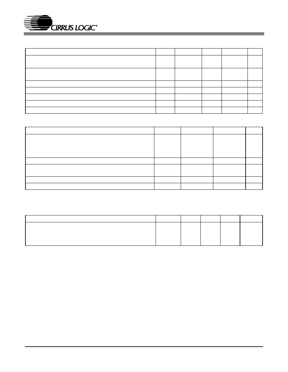
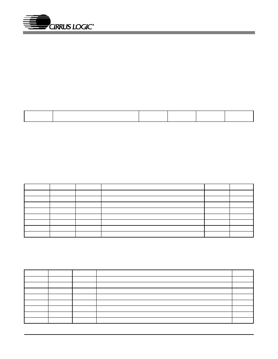
SWITCHING CHARACTERISTICS
(For KQZ T
A
= -10 to +70 ∞C; VLS = 1.8 V to 5.5 V; Inputs: Logic
0 = GND, Logic 1 = VLS, C
L
= 30 pF)
Notes: 15. See Table 5 on page 26 for suggested MCLK frequencies
16. This serial clock is available only in Control Port Mode when the MCLK Divide bit is enabled.
17. The higher frequency LRCK must be an exact integer multiple (1, 2, or 4) of the lower frequency LRCK
.
Parameters
Symbol
Min Typ
Max
Units
MCLK Frequency
(Note 15)
Single Speed Mode
1.024
-
51.2
MHz
Double Speed Mode
6.400
-
51.2
MHz
Quad Speed Mode
6.400
-
51.2
MHz
MCLK Duty Cycle
40
50
60
%
Input Sample Rate
Single Speed Mode
Double Speed Mode
Quad Speed Mode
Fs
Fs
Fs
4
50
100
-
-
-
50
100
200
kHz
kHz
kHz
LRCK Duty Cycle
45
50
55
%
SCLK Pulse Width Low
t
sclkl
20
-
-
ns
SCLK Pulse Width High
t
sclkh
20
-
-
ns
SCLK Period
t
sclkw
-
-
ns
(Note 16)
t
sclkw
-
-
ns
SCLK rising to LRCK edge delay
t
slrd
20
-
-
ns
SCLK rising to LRCK edge setup time
t
slrs
20
-
-
ns
SDATA valid to SCLK rising setup time
t
sdlrs
20
-
-
ns
SCLK rising to SDATA hold time
t
sdh
20
-
-
ns
LRCK1 to LRCK2 frequency ratio
(Note 17)
0.25
1.00
4.00
2
MCLK
------------------
4
MCLK
------------------
sclkh
t
slrs
t
slrd
t
sd lrs
t
sd h
t
sclkl
t
S D A TA
S C L K
L R C K
Figure 1. Serial Mode Input Timing
CS4382
DS514F1
9
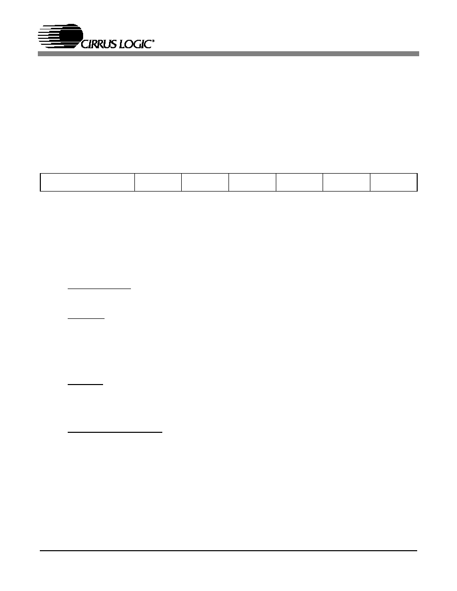
DSD - SWITCHING CHARACTERISTICS
(For KQZ T
A
= -10 to +70 ∞C; Logic 0 = GND; VLS =
1.8 V to 5.5 V; Logic 1 = VLS Volts; C
L
= 30 pF)
Note: 18. Min is 4 times 64x DSD or 2 times 128x DSD, and Max is 12 times 64x DSD or 6 times 128x DSD. The
proper MCLK to DSD_SCLK ratio must be set either by the DIF registers or the M0:2 pins
Parameter
Symbol Min Typ
Max
Unit
Master Clock Frequency
(Note 18)
4.096
-
38.4
MHz
MCLK Duty Cycle (All DSD modes)
40
50
60
%
DSD_SCLK Pulse Width Low
t
sclkl
20
-
-
ns
DSD_SCLK Pulse Width High
t
sclkh
20
-
-
ns
DSD_SCLK Frequency (64x Oversampled)
(128x Oversampled)
1.024
2.048
-
-
3.2
6.4
MHz
MHz
DSD_L / _R valid to DSD_SCLK rising setup time
t
sdlrs
20
-
-
ns
DSD_SCLK rising to DSD_L or DSD_R hold time
t
sdh
20
-
-
ns
s c lkh
t
sclkl
t
D S D _L, D S D _R
D S D _ S C L K
s d lrs
t
s d h
t
Figure 2. Direct Stream Digital - Serial Audio Input Timing
CS4382
10
DS514F1
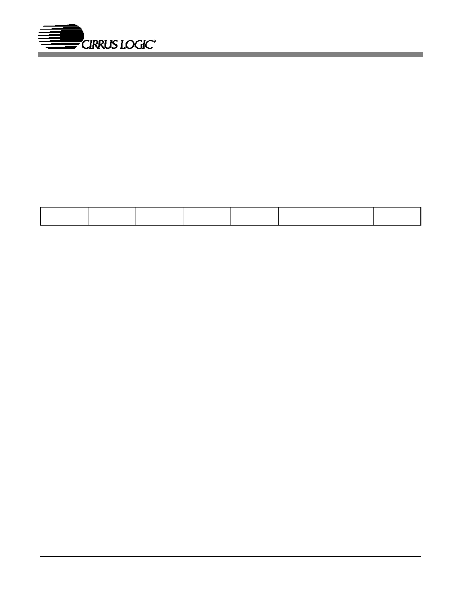
SWITCHING CHARACTERISTICS - CONTROL PORT - I
2
C FORMAT
(For KQZ T
A
= -10 to +70 ∞C; VLC = 1.8 V to 5.5 V; Inputs: Logic 0 = GND, Logic 1 = VLC, C
L
= 30 pF)
Notes: 19. Data must be held for sufficient time to bridge the transition time, t
fc
, of SCL.
20. The acknowledge delay is based on MCLK and can limit the maximum transaction speed.
21.
for Single-Speed Mode,
for Double-Speed Mode,
for Quad-Speed Mode.
Parameter
Symbol
Min
Max
Unit
SCL Clock Frequency
f
scl
-
100
kHz
RST Rising Edge to Start
t
irs
500
-
ns
Bus Free Time Between Transmissions
t
buf
4.7
-
µs
Start Condition Hold Time (prior to first clock pulse)
t
hdst
4.0
-
µs
Clock Low time
t
low
4.7
-
µs
Clock High Time
t
high
4.0
-
µs
Setup Time for Repeated Start Condition
t
sust
4.7
-
µs
SDA Hold Time from SCL Falling
(Note 19)
t
hdd
0
-
µs
SDA Setup time to SCL Rising
t
sud
250
-
ns
Rise Time of SCL and SDA
t
rc
, t
rc
-
1
µs
Fall Time SCL and SDA
t
fc
, t
fc
-
300
ns
Setup Time for Stop Condition
t
susp
4.7
-
µs
Acknowledge Delay from SCL Falling
(Note 20)
t
ack
-
(Note 21)
ns
15
256 Fs
◊
---------------------
15
128 Fs
◊
---------------------
15
64 Fs
◊
------------------
SDA
SCL
001100
ADDR
AD0
R/W
Start
ACK
DATA
1-8
ACK
DATA
1-8
ACK
Stop
Note: If operation is a write, this byte contains the Memory Address Pointer, MAP.
Note 1
Figure 3. Control Port Timing - I
2
C Format

CS4382
DS514F1
11
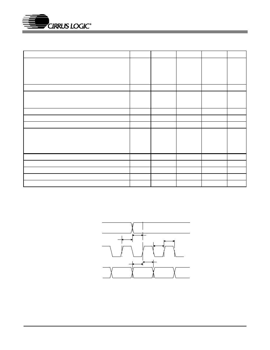
SWITCHING CHARACTERISTICS - CONTROL PORT - SPI
TM
FORMAT
(For KQZ T
A
= -10 to +70 ∞C; VLC = 1.8 V to 5.5 V; Inputs: Logic 0 = GND, Logic 1 = VLC, C
L
= 30 pF)
Notes: 22. t
spi
only needed before first falling edge of CS after RST rising edge. t
spi
= 0 at all other times.
23. Data must be held for sufficient time to bridge the transition time of CCLK.
24. For F
SCK
< 1 MHz.
Parameter
Symbol
Min
Max
Unit
CCLK Clock Frequency
f
sclk
-
MHz
RST Rising Edge to CS Falling
t
srs
500
-
ns
CCLK Edge to CS Falling
(Note 22)
t
spi
500
-
ns
CS High Time Between Transmissions
t
csh
1.0
-
µs
CS Falling to CCLK Edge
t
css
20
-
ns
CCLK Low Time
t
scl
-
ns
CCLK High Time
t
sch
-
ns
CDIN to CCLK Rising Setup Time
t
dsu
40
-
ns
CCLK Rising to DATA Hold Time
(Note 23)
t
dh
15
-
ns
Rise Time of CCLK and CDIN
(Note 24)
t
r2
-
100
ns
Fall Time of CCLK and CDIN
(Note 24)
t
f2
-
100
ns
MCLK
2
------------------
1
MCLK
------------------
1
MCLK
------------------
t r2
t f2
t dsu t dh
t sch
t scl
C S
C C L K
C D IN
t css
t csh
t spi
t srs
R S T
Figure 4. Control Port Timing - SPI Format

CS4382
12
DS514F1
Figure 5. Typical Connection Diagram Control Port
D igital
A udio
S ource
V LS
C S 4 3 82
M C LK
V D
A O U T A 1+
10
8
32
0.1 µ F
+
1 µ F
+3.3 V to +5 V
S D IN 1
9
1 µ F
0.1 µ F
+
+
20
21
F ILT +
V Q
7
6
LR C K 1
S C LK 1
S D IN 3
S D IN 2
39
40
0.1 µ F
47 µ F
V A
0.1 µ F
+
1 µ F
0.1 µ F
+ 1.8 V to +5 V
+5 V
4
43
S D IN 4
LR C K 2
S C LK 2
13
14
A nalog C onditio ning
an d M uting
A O U T A 1-
A O U T B 1+ 38
37
A nalog C onditio ning
an d M uting
A O U T B 1-
A O U T A 2+
35
36
A nalog C onditio ning
an d M uting
A O U T A 2-
A O U T B 2+ 34
33
A nalog C onditio ning
an d M uting
A O U T B 2-
A O U T A 3+
29
30
A nalog C onditio ning
an d M uting
A O U T A 3-
A O U T B 3+
28
27
A nalog C onditio ning
an d M uting
A O U T B 3-
A O U T A 4+ 25
26
A nalog C onditio ning
an d M uting
A O U T A 4-
A O U T B 4+
24
23
A nalog C onditio ning
an d M uting
A O U T B 4-
M U T E C 1
41
22
M ute
D rive
M U T E C 234
11
12
P C M
31
G N D
G N D
5
M icro-
C ontroller
V LC
0.1 µ F
+ 1.8 V to +5 V
18
D S D
A udio
S ource
2
48
D S D B 2
3
42
D S D _S C LK
D S D A 1
D S D B 3
D S D A 3
D S D A 4
D S D B 1
D S D A 2
46
45
47
1
44
D S D B 4
16
15
S C L/C C LK
S D A /C D IN
A D O /C S
R S T
19
17
2 K
2 K
N ote: N ecessary for I
2
C
control port operation
N ote*
CS4382
DS514F1
13
D ig ita l
A u d io
S o u rc e
V L S
C S 4 3 8 2
M C L K
V D
A O U T A 1 +
1 0
8
3 2
0 .1 µ F
+
1 µ F
+ 3 .3 V to + 5 V
S D IN 1
9
1 µ F
0 .1 µ F
+
+
2 0
2 1
F IL T +
V Q
7
6
L R C K 1
S C L K 1
S D IN 3
S D IN 2
3 9
4 0
0 .1 µ F
4 7 µ F
V A
0 .1 µ F
+
1 µ F
0 .1 µ F
+ 1 .8 V to + 5 V
+ 5 V
4
4 3
S D IN 4
L R C K 2
S C L K 2
1 3
1 4
A n a lo g C o n d itio n in g
a n d M u tin g
A O U T A 1 -
A O U T B 1 + 3 8
3 7
A n a lo g C o n d itio n in g
a n d M u tin g
A O U T B 1 -
A O U T A 2 +
3 5
3 6
A n a lo g C o n d itio n in g
a n d M u tin g
A O U T A 2 -
A O U T B 2 + 3 4
3 3
A n a lo g C o n d itio n in g
a n d M u tin g
A O U T B 2 -
A O U T A 3 + 2 9
3 0
A n a lo g C o n d itio n in g
a n d M u tin g
A O U T A 3 -
A O U T B 3 +
2 8
2 7
A n a lo g C o n d itio n in g
a n d M u tin g
A O U T B 3 -
A O U T A 4 + 2 5
2 6
A n a lo g C o n d itio n in g
a n d M u tin g
A O U T A 4 -
A O U T B 4 +
2 4
2 3
A n a lo g C o n d itio n in g
a n d M u tin g
A O U T B 4 -
M U T E C 2 3 4
2 2
4 1
M u te
D rive
M U T E C 1
1 1
1 2
P C M
3 1
G N D
G N D
5
S ta n d -A lo n e
M o d e
C o n fig u ra tio n
V L C
0 .1 µ F
+ 1 .8 V to + 5 V
1 8
D S D
A u d io
S o u rc e
2
4 8
D S D B 2
3
4 2
M 3 (D S D _ S C L K )
D S D A 1
D S D B 3
D S D A 3
D S D A 4
D S D B 1
D S D A 2
4 6
4 5
4 7
1
4 4
D S D B 4
1 6
1 5
M 2
M 1
M 0
R S T
1 9
1 7
4 7 K
V L S
N o te
D S D
N o te
D S D
: F o r D S D o p e ra tio n :
1 ) L R C K 1 m u s t b e tie d to V L S a n d
re m a in s ta tic h ig h .
2 ) M 3 P C M s ta n d -a lo n e c o n fig u ra tio n
p in b e c o m e s D S D _ S C L K
M u te
D rive
4 7 K
N o te
D S D
N o te
V L C
N o te
V L C
: If s e rie s re s is to rs a re
u s e d th e y m u s t b e < 1 k O h m . If
p o s s ib le tie V L C to th e V D s u p p ly
to re d u c e p o s s ib le e xc e s s c u rre n t
c o n s u m p tio n fro m V L C .
Figure 6. Typical Connection Diagram Stand-Alone
CS4382
14
DS514F1
2.
REGISTER QUICK REFERENCE
Addr
Function
7
6
5
4
3
2
1
0
01h Mode Control 1
CPEN
FREEZE
MCLKDIV
DAC4_DIS DAC3_DIS DAC2_DIS DAC1_DIS
PDN
default
0
0
0
0
0
0
0
1
02h Mode Control 2
Reserved
DIF2
DIF1
DIF0
SDIN4CLK SDIN3CLK SDIN2CLK SDIN1CLK
default
0
0
0
0
0
0
0
0
03h Mode Control 3
SZC1
SZC0
SNGLVOL
RMP_UP
MUTEC+/-
AMUTE
Reserved
MUTEC
default
1
0
0
0
0
1
0
0
04h Filter Control
Reserved
Reserved
Reserved
FILT_SEL
Reserved
DEM1
DEM0
RMP_DN
default
0
0
0
0
0
0
0
0
05h Invert Control
INV_B4
INV_A4
INV_B3
INV_A3
INV_B2
INV_A2
INV_B1
INV_A1
default
0
0
0
0
0
0
0
0
06h Mixing Control
Pair 1 (AOUTx1)
P1_A=B
P1ATAPI4 P1ATAPI3 P1ATAPI2 P1ATAPI1 P1ATAPI0
P1FM1
P1FM0
default
0
0
1
0
0
1
0
0
07h Vol. Control A1
A1_MUTE
A1_VOL6
A1_VOL5
A1_VOL4
A1_VOL3
A1_VOL2
A1_VOL1
A1_VOL0
default
0
0
0
0
0
0
0
0
08h Vol. Control B1
B1_MUTE
B1_VOL6
B1_VOL5
B1_VOL4
B1_VOL3
B1_VOL2
B1_VOL1
B1_VOL0
default
0
0
0
0
0
0
0
0
09h Mixing Control
Pair 2 (AOUTx2)
P2_A=B
P2ATAPI4 P2ATAPI3 P2ATAPI2 P2ATAPI1 P2ATAPI0
P2FM1
P2FM0
default
0
0
1
0
0
1
0
0
0Ah Vol. Control A2
A2_MUTE
A2_VOL6
A2_VOL5
A2_VOL4
A2_VOL3
A2_VOL2
A2_VOL1
A2_VOL0
default
0
0
0
0
0
0
0
0
0Bh Vol. Control B2
B2_MUTE
B2_VOL6
B2_VOL5
B2_VOL4
B2_VOL3
B2_VOL2
B2_VOL1
B2_VOL0
default
0
0
0
0
0
0
0
0
0Ch Mixing Control
Pair 3 (AOUTx3)
P3_A=B
P3ATAPI4 P3ATAPI3 P3ATAPI2 P3ATAPI1 P3ATAPI0
P3FM1
P3FM0
default
0
0
1
0
0
1
0
0
0Dh Vol. Control A3
A3_MUTE
A3_VOL6
A3_VOL5
A3_VOL4
A3_VOL3
A3_VOL2
A3_VOL1
A3_VOL0
default
0
0
0
0
0
0
0
0
0Eh Vol. Control B3
B3_MUTE
B3_VOL6
B3_VOL5
B3_VOL4
B3_VOL3
B3_VOL2
B3_VOL1
B3_VOL0
default
0
0
0
0
0
0
0
0
0Fh Mixing Control
Pair 4 (AOUTx4)
P4_A=B
P4ATAPI4 P4ATAPI3 P4ATAPI2 P4ATAPI1 P4ATAPI0
P4FM1
P4FM0
default
0
0
1
0
0
1
0
0
10h Vol. Control A4
A4_MUTE
A4_VOL6
A4_VOL5
A4_VOL4
A4_VOL3
A4_VOL2
A4_VOL1
A4_VOL0
default
0
0
0
0
0
0
0
0
11h Vol. Control B4
B4_MUTE
B4_VOL6
B4_VOL5
B4_VOL4
B4_VOL3
B4_VOL2
B4_VOL1
B4_VOL0
default
0
0
0
0
0
0
0
0
12h Chip Revision
PART3
PART2
PART1
PART0
Reserved
Reserved
Reserved
Reserved
default
1
0
1
0
-
-
-
-
CS4382
DS514F1
15
3.
REGISTER DESCRIPTION
Note:
All registers are read/write in I
2
C mode and write only in SPI, unless otherwise noted.
3.1
Mode Control 1 (address 01h)
3.1.1 CONTROL PORT ENABLE (CPEN)
Default = 0
0 - Disabled
1 - Enabled
Function
:
This bit defaults to 0, allowing the device to power-up in Stand-Alone mode. The Control port mode
can be accessed by setting this bit to 1. This will allow the operation of the device to be controlled by
the registers and the pin definitions will conform to Control Port Mode. To accomplish a clean power-
up, the user should write this bit within 10 ms following the release of Reset.
3.1.2 FREEZE CONTROLS (FREEZE)
Default = 0
0 - Disabled
1 - Enabled
Function:
This function allows modifications to be made to the registers without the changes taking effect until
the FREEZE is disabled. To make multiple changes in the Control port registers take effect simulta-
neously, enable the FREEZE Bit, make all register changes, then Disable the FREEZE bit.
3.1.3 MASTER CLOCK DIVIDE ENABLE (MCLKDIV)
Default = 0
0 - Disabled
1 - Enabled
Function:
The MCLKDIV bit enables a circuit which divides the externally applied MCLK signal by 2 prior to all
other internal circuitry.
3.1.4 DAC PAIR DISABLE (DACX_DIS)
Default = 0
0 - Enabled
1 - Disabled
Function:
When enabled the respective DAC channel pair x (AOUTAx and AOUTBx) will remain in a reset state.
It is advised that changes to these bits be made while the power down bit is enabled to eliminate the
possibility of audible artifacts.
7
6
5
4
3
2
1
0
CPEN
FREEZE
MCLKDIV
DAC4_DIS
DAC3_DIS
DAC2_DIS
DAC1_DIS
PDN
0
0
0
0
0
0
0
1
CS4382
16
DS514F1
3.1.5 POWER DOWN (PDN)
Default = 1
0 - Disabled
1 - Enabled
Function:
The entire device will enter a low-power state when this function is enabled, and the contents of the
control registers are retained in this mode. The power-down bit defaults to `enabled' on power-up and
must be disabled before normal operation in Control Port mode can occur.
3.2
Mode Control 2 (address 02h)
3.2.1 DIGITAL INTERFACE FORMAT (DIF)
Default = 000 - Format 0 (Left Justified, up to 24-bit data)
Function:
These bits select the interface format for the serial audio input. The Functional Mode bits determine
whether PCM or DSD mode is selected.
PCM Mode: The required relationship between the Left/Right clock, serial clock and serial data is defined
by the Digital Interface Format and the options are detailed in Figures 33-38.
DSD Mode: The relationship between the oversampling ratio of the DSD audio data and the required
Master clock to DSD data rate is defined by the Digital Interface Format pins. An additional write of 99h
to register 00h and 80h to register 1Ah is required to access the modes denoted with *.
7
6
5
4
3
2
1
0
Reserved
DIF2
DIF1
DIF0
SDIN4CLK
SDIN3CLK
SDIN2CLK
SDIN1CLK
0
0
0
0
0
0
0
0
DIF2
DIF1
DIF0
DESCRIPTION
Format
FIGURE
0
0
0
Left Justified, up to 24-bit data
0
33
0
0
1
I
2
S, up to 24-bit data
1
34
0
1
0
Right Justified, 16-bit data
2
35
0
1
1
Right Justified, 24-bit data
3
36
1
0
0
Right Justified, 20-bit data
4
37
1
0
1
Right Justified, 18-bit data
5
38
1
1
0
Reserved
1
1
1
Reserved
Table 1. Digital Interface Formats - PCM Mode
DIF2
DIF1
DIFO
DESCRIPTION
Note
0
0
0
64x oversampled DSD data with a 4x MCLK to DSD data rate
0
0
1
64x oversampled DSD data with a 6x MCLK to DSD data rate
*
0
1
0
64x oversampled DSD data with a 8x MCLK to DSD data rate
*
0
1
1
64x oversampled DSD data with a 12x MCLK to DSD data rate
*
1
0
0
128x oversampled DSD data with a 2x MCLK to DSD data rate
1
0
1
128x oversampled DSD data with a 3x MCLK to DSD data rate
*
1
1
0
128x oversampled DSD data with a 4x MCLK to DSD data rate
*
1
1
1
128x oversampled DSD data with a 6x MCLK to DSD data rate
*
Table 2. Digital Interface Formats - DSD Mode
CS4382
DS514F1
17
3.2.2 SERIAL AUDIO DATA CLOCK SOURCE (SDINXCLK)
Default = 0
0 - SDINx clocked by SCLK1 and LRCK1
1 - SDINx clocked by SCLK2 and LRCK2
Function:
The SDINxCLK bit specifies which SCLK/LRCK input pair is used to clock in the data on the given
SDINx line. For more details see "Clock Source Selection" on page 28.
3.3
Mode Control 3 (address 03h)
3.3.1 SOFT RAMP AND ZERO CROSS CONTROL (SZC)
Default = 10
00 - Immediate Change
01 - Zero Cross
10 - Soft Ramp
11 - Soft Ramp on Zero Crossings
Function:
Immediate Change
When Immediate Change is selected all level changes will take effect immediately in one step.
Zero Cross
Zero Cross Enable dictates that signal level changes, either by attenuation changes or muting, will
occur on a signal zero crossing to minimize audible artifacts. The requested level change will occur
after a timeout period between 512 and 1024 sample periods (10.7 ms to 21.3 ms at 48 kHz sample
rate) if the signal does not encounter a zero crossing. The zero cross function is independently mon-
itored and implemented for each channel.
Soft Ramp
Soft Ramp allows level changes, both muting and attenuation, to be implemented by incrementally
ramping, in 1/8 dB steps, from the current level to the new level at a rate of 1 dB per 8 left/right clock
periods.
Soft Ramp on Zero Crossing
Soft Ramp and Zero Cross Enable dictates that signal level changes, either by attenuation changes
or muting, will occur in 1/8 dB steps and be implemented on a signal zero crossing. The 1/8 dB level
change will occur after a timeout period between 512 and 1024 sample periods (10.7 ms to 21.3 ms
at 48 kHz sample rate) if the signal does not encounter a zero crossing. The zero cross function is
independently monitored and implemented for each channel.
7
6
5
4
3
2
1
0
SZC1
SZC0
SNGLVOL
RMP_UP
Reserved
AMUTE
Reserved
MUTEC
1
0
0
0
0
1
0
0

CS4382
18
DS514F1
3.3.2 SINGLE VOLUME CONTROL (SNGLVOL)
Default = 0
0 - Disabled
1 - Enabled
Function:
The individual channel volume levels are independently controlled by their respective Volume Control
Bytes when this function is disabled. The volume on all channels is determined by the A1 Channel
Volume Control Byte, and the other Volume Control Bytes are ignored when this function is enabled.
3.3.3 SOFT VOLUME RAMP-UP AFTER ERROR (RMP_UP)
Default = 0
0 - Disabled
1 - Enabled
Function:
An un-mute will be performed after executing a filter mode change, after a LRCK/MCLK ratio change
or error, and after changing the Functional Mode. When this feature is enabled, this un-mute is ef-
fected, similar to attenuation changes, by the Soft and Zero Cross bits in the Mode Control 3 register.
When disabled, an immediate un-mute is performed in these instances.
Note: For best results, it is recommended that this feature be used in conjunction with the RMP_DN
bit.
3.3.4 MUTEC POLARITY (MUTEC+/-)
Default = 0
0 - Active High
1 - Active Low
Function:
The active polarity of the MUTEC pin(s) is determined by this register. When set to 0 (default) the
MUTEC pins are high when active. When set to 1 the MUTEC pin(s) are low when active.
Note: When the on board mute circuitry is designed for active low, the MUTEC outputs will be high
(un-muted) for the period of time during reset and before this bit is enabled to 1.
3.3.5 AUTO-MUTE (AMUTE)
Default = 1
0 - Disabled
1 - Enabled
Function:
The Digital-to-Analog converter output will mute following the reception of 8192 consecutive audio
samples of static 0 or -1. A single sample of non-static data will release the mute. Detection and
muting is done independently for each channel. The quiescent voltage on the output will be retained
and the Mute Control pin will go active during the mute period. The muting function is affected, similar
to volume control changes, by the Soft and Zero Cross bits in the Mode Control 3 register.
CS4382
DS514F1
19
3.3.6 MUTEC PIN CONTROL(MUTEC)
Default = 0
0 - Two Mute control signals
1 - Single mute control signal on MUTEC1
Function:
Selects how the internal mute signals are routed to the MUTEC1 and MUTEC234 pins. When set to
`0', a logical AND of DAC pair 1 mute control signals are output on MUTEC1 and a logical AND of the
mute control signals of DAC pairs 2, 3, and 4 are output on MUTEC234. When set to `1', a logical AND
of all DAC pair mute control signals is output on the MUTEC1 pin, MUTEC234 will remain static. For
more information on the use of the mute control function see the MUTEC1 and MUTEC234 pins in
section 4.
3.4
Filter Control (address 04h)
3.4.1 INTERPOLATION FILTER SELECT (FILT_SEL)
Default = 0
0 - Fast roll-off
1 - Slow roll-off
Function
:
This Function allows the user to select whether the interpolation filter has a fast or slow roll off. For
filter characteristics please see Section 1.
3.4.2 DE-EMPHASIS CONTROL (DEM)
Default = 00
00 - Disabled
01 - 44.1 kHz
10 - 48 kHz
11 - 32 kHz
Function:
Selects the appropriate digital filter to maintain the standard 15
µ
s/50
µ
s digital de-emphasis filter re-
sponse at 32, 44.1 or 48 kHz sample rates. (see Figure 39)
De-emphasis is only available in Single Speed Mode.
7
6
5
4
3
2
1
0
Reserved
Reserved
Reserved
FILT_SEL
Reserved
DEM1
DEM0
RMP_DN
0
0
0
0
0
0
0
0

CS4382
20
DS514F1
3.4.3 SOFT RAMP-DOWN BEFORE FILTER MODE CHANGE (RMP_DN)
Default = 0
0 - Disabled
1 - Enabled
Function:
A mute will be performed prior to executing a filter mode change. When this feature is enabled, this
mute is effected, similar to attenuation changes, by the Soft and Zero Cross bits in the Mode Control
3 register. When disabled, an immediate mute is performed prior to executing a filter mode change.
Note: For best results, it is recommended that this feature be used in conjunction with the RMP_UP
bit.
3.5
Invert control (address 05h)
3.5.1 INVERT SIGNAL POLARITY (INV_XX)
Default = 0
0 - Disabled
1 - Enabled
Function:
When enabled, these bits will invert the signal polarity of their respective channels.
3.6
Mixing Control Pair 1 (Channels A1 & B1)(address 06h)
Mixing Control Pair 2 (Channels A2 & B2)(address 09h)
Mixing Control Pair 3 (Channels A3 & B3)(address 0Ch)
Mixing Control Pair 4 (Channels A4 & B4)(address 0Fh)
3.6.1 CHANNEL A VOLUME = CHANNEL B VOLUME (A=B)
Default = 0
0 - Disabled
1 - Enabled
Function:
The AOUTAx and AOUTBx volume levels are independently controlled by the A and the B Channel
Volume Control Bytes when this function is disabled. The volume on both AOUTAx and AOUTBx are
determined by the A Channel Attenuation and Volume Control Bytes (per A-B pair), and the B Chan-
nel Bytes are ignored when this function is enabled.
7
6
5
4
3
2
1
0
INV_B4
INV_A4
INV_B3
INV_A3
INV_B2
INV_A2
INV_B1
INV_A1
0
0
0
0
0
0
0
0
7
6
5
4
3
2
1
0
Px_A=B
PxATAPI4
PxATAPI3
PxATAPI2
PxATAPI1
PxATAPI0
PxFM1
PxFM0
0
0
1
0
0
1
0
0
CS4382
DS514F1
21
3.6.2 ATAPI CHANNEL MIXING AND MUTING (ATAPI)
Default = 01001 - AOUTAx=aL, AOUTBx=bR (Stereo)
Function:
The CS4382 implements the channel mixing functions of the ATAPI CD-ROM specification. The ATAPI
functions are applied per A-B pair. Refer to Table 3 and Figure 41 for additional information
.
ATAPI4 ATAPI3 ATAPI2 ATAPI1 ATAPI0
AOUTAx
AOUTBx
0
0
0
0
0
MUTE
MUTE
0
0
0
0
1
MUTE
bR
0
0
0
1
0
MUTE
bL
0
0
0
1
1
MUTE
b[(L+R)/2]
0
0
1
0
0
aR
MUTE
0
0
1
0
1
aR
bR
0
0
1
1
0
aR
bL
0
0
1
1
1
aR
b[(L+R)/2]
0
1
0
0
0
aL
MUTE
0
1
0
0
1
aL
bR
0
1
0
1
0
aL
bL
0
1
0
1
1
aL
b[(L+R)/2]
0
1
1
0
0
a[(L+R)/2]
MUTE
0
1
1
0
1
a[(L+R)/2]
bR
0
1
1
1
0
a[(L+R)/2]
bL
0
1
1
1
1
a[(L+R)/2]
b[(L+R)/2]
1
0
0
0
0
MUTE
MUTE
1
0
0
0
1
MUTE
bR
1
0
0
1
0
MUTE
bL
1
0
0
1
1
MUTE
[(aL+bR)/2]
1
0
1
0
0
aR
MUTE
1
0
1
0
1
aR
bR
1
0
1
1
0
aR
bL
1
0
1
1
1
aR
[(bL+aR)/2]
1
1
0
0
0
aL
MUTE
1
1
0
0
1
aL
bR
1
1
0
1
0
aL
bL
1
1
0
1
1
aL
[(aL+bR)/2]
1
1
1
0
0
[(aL+bR)/2]
MUTE
1
1
1
0
1
[(aL+bR)/2]
bR
1
1
1
1
0
[(bL+aR)/2]
bL
1
1
1
1
1
[(aL+bR)/2]
[(aL+bR)/2]
Table 3. ATAPI Decode

CS4382
22
DS514F1
3.6.3 FUNCTIONAL MODE (FM)
Default = 00
00 - Single-Speed Mode (4 to 50 kHz sample rates)
01 - Double-Speed Mode (50 to 100 kHz sample rates)
10 - Quad-Speed Mode (100 to 200 kHz sample rates)
11 - Direct Stream Digital Mode
Function:
Selects the required range of input sample rates or DSD Mode. When DSD mode is selected for any
channel pair then all pairs will switch to DSD mode.
3.7
Volume control (addresses 07h, 08h, 0Ah, 0Bh, 0Dh, 0Eh, 10h, 11h)
3.7.1 MUTE (MUTE)
Default = 0
0 - Disabled
1 - Enabled
Function:
The Digital-to-Analog converter output will mute when enabled. The quiescent voltage on the output
will be retained. The muting function is effected, similar to attenuation changes, by the Soft and Zero
Cross bits. The MUTEC pins will go active during the mute period according to the MUTEC register.
3.7.2 VOLUME CONTROL (XX_VOL)
Default = 0 (No attenuation)
Function:
The Digital Volume Control registers allow independent control of the signal levels in 1 dB increments
from 0 to -127 dB. Volume settings are decoded as shown in Table 4. The volume changes are imple-
mented as dictated by the Soft and Zero Cross bits. All volume settings less than -127 dB are equivalent
to enabling the MUTE bit.
7
6
5
4
3
2
1
0
xx_MUTE
xx_VOL6
xx_VOL5
xx_VOL4
xx_VOL3
xx_VOL2
xx_VOL1
xx_VOL0
0
0
0
0
0
0
0
0
Binary Code
Decimal Value
Volume Setting
0000000
0
0 dB
0010100
20
-20 dB
0101000
40
-40 dB
0111100
60
-60 dB
1011010
90
-90 dB
Table 4. Example Digital Volume Settings

CS4382
DS514F1
23
3.8
Chip Revision (address 12h)
3.8.1 PART NUMBER ID (PART) [READ ONLY]
1010 - CS4382
Function:
This read-only register can be used to identify the model number of the device.
7
6
5
4
3
2
1
0
PART3
PART2
PART1
PART0
Reserved
Reserved
Reserved
Reserved
1
0
1
0
-
-
-
-

CS4382
24
DS514F1
4.
PIN DESCRIPTION
Pin Name
#
Pin Description
VD
4
Digital Power (Input) - Positive power supply for the digital section. Refer to the Recommended Operat-
ing Conditions for appropriate voltages.
GND
5
31
Ground (Input) - Ground reference. Should be connected to analog ground.
MCLK
6
Master Clock (Input) - Clock source for the delta-sigma modulator and digital filters. Table 5 illustrates
several standard audio sample rates and the required master clock frequency.
LRCK1
LRCK2
7
10
Left Right Clock (Input) - Determines which channel, Left or Right, is currently active on the serial audio
data line. The frequency of the left/right clock must be at the audio sample rate, Fs.
SDIN1
SDIN2
SDIN3
SDIN4
8
11
13
14
Serial Audio Data Input (Input) - Input for two's complement serial audio data.
SCLK1
SCLK2
9
12
Serial Clock (Input) - Serial clock for the serial audio interface.
VLC
18
Control Port Power (Input) - Determines the required signal level for the control port. Refer to the Rec-
ommended Operating Conditions for appropriate voltages.
RST
19
Reset (Input) - The device enters a low power mode and all internal registers are reset to their default
settings when low.
FILT+
20
Positive Voltage Reference (Output) - Positive reference voltage for the internal sampling circuits.
Requires the capacitive decoupling to analog ground, as shown in the Typical Connection Diagram.
VQ
21
Quiescent Voltage (Output) - Filter connection for internal quiescent voltage. VQ must be capacitively
coupled to analog ground, as shown in the Typical Connection Diagram. The nominal voltage level is
specified in the Analog Characteristics and Specifications section. VQ presents an appreciable source
impedance and any current drawn from this pin will alter device performance. However, VQ can be
used to bias the analog circuitry assuming there is no AC signal component and the DC current is less
than the maximum specified in the Analog Characteristics and Specifications section.
SD
I
N
3
GND
AOUTB2-
AOUTA3+
AOUTB3-
AOUTB2+
VA
AOUTA3-
AOUTB3+
6
2
4
8
1 0
1
3
5
7
9
1 1
1 2
1 3 1 4 1 5 1 6 1 7 1 8 1 9 2 0 2 1 2 2 2 3 2 4
3 1
35
33
29
27
36
34
32
30
28
26
25
4 8 4 7 4 6 4 5 4 4 4 3 4 2 4 1 4 0 3 9 3 8 3 7
MCLK
DSDB1
VD
SDIN1
LRCK2
DSDA2
DSDA1
GND
SCLK1
SDIN2
SCLK2
LRCK1(DSD_EN)
M
3
(
D
SD
_
S
C
L
K)
DS
DB
3
DS
DA
3
DS
DA
4
CS4382
DS
DB
4
VLS
SD
I
N
4
M
2
(
S
CL
/
CCL
K
)
M
1
(
S
DA/
CDI
N)
VL
C
RS
T
FI
LT+
VQ
MU
T
E
C
2
3
4
M0
(
A
D
0
/
C
S
)
AOUTA2+
AOUTA2-
AO
UT
B
1
+
AO
U
T
B1
-
AO
U
T
A1-
AO
U
T
A1
+
DS
DB
2
MU
T
E
C
1
AOUTA4-
AOUTA4+
AO
U
T
B4+
AO
U
T
B4
-

CS4382
DS514F1
25
MUTEC1
MUTEC234
41
22
Mute Control (Output) - The Mute Control pins go high during power-up initialization, reset, muting,
power-down or if the master clock to left/right clock frequency ratio is incorrect. These pins are intended
to be used as a control for external mute circuits to prevent the clicks and pops that can occur in any sin-
gle supply system. The use of external mute circuits are not mandatory but may be desired for designs
requiring the absolute minimum in extraneous clicks and pops.
AOUTA1 +,-
AOUTB1 +,-
AOUTA2 +,-
AOUTB2 +,-
AOUTA3 +,-
AOUTB3 +,-
AOUTA4 +,-
AOUTB4 +,-
39, 40
38, 37
35, 36
34, 33
29, 30
28, 27
25, 26
24, 23
Differential Analog Output (Output) - The full scale differential analog output level is specified in the
Analog Characteristics specification table.
VA
32
Analog Power (Input) - Positive power supply for the analog section. Refer to the Recommended Oper-
ating Conditions for appropriate voltages.
VLS
43
Serial Audio Interface Power (Input) - Determines the required signal level for the serial audio inter-
face. Refer to the Recommended Operating Conditions for appropriate voltages.
Control Port Definitions
SCL/CCLK
15
Serial Control Port Clock (Input) - Serial clock for the serial control port. Requires an external pull-up
resistor to the logic interface voltage in I
2
C mode as shown in the Typical Connection Diagram.
SDA/CDIN
16
Serial Control Data (Input/Output) - SDA is a data I/O line in I
2
C mode and requires an external pull-up
resistor to the logic interface voltage, as shown in the Typical Connection Diagram. CDIN is the input
data line for the control port interface in SPI mode.
AD0/CS
17
Address Bit 0 (I
2
C) / Control Port Chip Select (SPI) (Input) - AD0 is a chip address pin in I
2
C mode;
CS is the chip select signal for SPI format.
Stand-Alone Definitions
M0
M1
M2
M3
17
16
15
42
Mode Selection (Input) - Determines the operational mode of the device as detailed in Tables 6 and 7.
DSD Definitions
DSD_SCLK
42
DSD Serial Clock (Input) - Serial clock for the Direct Stream Digital audio interface.
DSD_EN
7
DSD-Enable (Input) - When held at logic `1' the device will enter DSD mode (Stand-Alone mode only).
DSDA1
DSDB1
DSDA2
DSDB2
DSDA3
DSDB3
DSDA4
DSDB4
3
2
1
48
47
46
45
44
Direct Stream Digital Input (Input) - Input for Direct Stream Digital serial audio data.
Pin Name
#
Pin Description
CS4382
26
DS514F1
*Note: These modes are only available in control port mode by setting the MCLKDIV bit = 1.
Mode
(sample-rate range)
Sample
Rate
(kHz)
MCLK (MHz)
Control port
only modes
MCLK Ratio
256x
384x
512x
768x*
1024x*
Single Speed
(4 to 50 kHz)
32
8.1920
12.2880
16.3840
24.5760
32.7680
44.1
11.2896
16.9344
22.5792
33.8688
45.1584
48
12.2880
18.4320
24.5760
36.8640
49.1520
MCLK Ratio
128x
192x
256x
384x
512x*
Double Speed
(50 to 100 kHz)
64
8.1920
12.2880
16.3840
24.5760
32.7680
88.2
11.2896
16.9344
22.5792
33.8688
45.1584
96
12.2880
18.4320
24.5760
36.8640
49.1520
MCLK Ratio
64x
96x
128x
192x
256x*
Quad Speed
(100 to 200 kHz)
176.4
11.2896
16.9344
22.5792
33.8688
45.1584
192
12.2880
18.4320
24.5760
36.8640
49.1520
Table 5. Common Clock Frequencies
M1
(DIF1)
M0
(DIF0)
DESCRIPTION
FORMAT
FIGURE
0
0
Left Justified, up to 24-bit data
0
33
0
1
I
2
S, up to 24-bit data
1
34
1
0
Right Justified, 16-bit Data
2
35
1
1
Right Justified, 24-bit Data
3
36
Table 6. Digital Interface Format, Stand-Alone Mode Options
M3
M2
(DEM)
DESCRIPTION
0
0
Single-Speed without De-Emphasis (4 to 50 kHz sample rates)
0
1
Single-Speed with 44.1 kHz De-Emphasis; see Figure 39
1
0
Double-Speed (50 to 100 kHz sample rates)
1
1
Quad-Speed (100 to 200 kHz sample rates)
Table 7. Mode Selection, Stand-Alone Mode Options
DSD_Mode
(LRCK1)
M2
M1
M0
DESCRIPTION
1
0
0
0
64x oversampled DSD data with a 4x MCLK to DSD data rate
1
0
0
1
Reserved
1
0
1
0
Reserved
1
0
1
1
Reserved
1
1
0
0
128x oversampled DSD data with a 2x MCLK to DSD data rate
1
1
0
1
Reserved
1
1
1
0
Reserved
1
1
1
1
Reserved
Table 8. Direct Stream Digital (DSD), Stand-Alone Mode Options

CS4382
DS514F1
27
5. APPLICATIONS
5.1
Grounding and Power Supply
Decoupling
As with any high resolution converter, the CS4382
requires careful attention to power supply and
grounding arrangements to optimize performance.
Figures 5 & 6 show the recommended power ar-
rangement with VA, VD, VLS and VLC connected
to clean supplies. Decoupling capacitors should be
located as close to the device package as possible.
If desired, all supply pins may be connected to the
same supply, but a decoupling capacitor should still
be placed on each supply pin (see Section 1 for rec-
ommended voltages).
5.2
Oversampling Modes
The CS4382 operates in one of three oversampling
modes based on the input sample rate. Mode selec-
tion is determined by the M3 and M2 pins in Stand-
Alone mode or the FM bits in Control Port mode.
Single-Speed mode supports input sample rates up
to 50 kHz and uses a 128x oversampling ratio.
Double-Speed mode supports input sample rates up
to 100 kHz and uses an oversampling ratio of 64x.
Quad-Speed mode supports input sample rates up
to 200 kHz and uses an oversampling ratio of 32x.
5.3
Recommended Power-up
Sequence
1. Hold RST low until the power supply, master,
and left/right clocks are stable. In this state, the
control port is reset to its default settings and VQ
will remain low.
2. Bring RST high. The device will remain in a low
power state with VQ low and will initiate the
Stand-Alone power-up sequence. The control port
will be accessible at this time. If Control Port oper-
ation is desired, write the CPEN bit prior to the
completion of the Stand-Alone power-up se-
quence, approximately 512 LRCK cycles in Sin-
gle-Speed Mode (1024 LRCK cycles in Double-
Speed Mode, and 2048 LRCK cycles in Quad-
Speed Mode). Writing this bit will halt the Stand-
Alone power-up sequence and initialize the control
port to its default settings. The desired register set-
tings can be loaded while keeping the PDN bit set
to 1.
3. If Control Port Mode is selected via the CPEN
bit, set the PDN bit to 0 which will initiate the pow-
er-up sequence.
5.4
Analog Output and Filtering
The application note "Design Notes for a 2-Pole
Filter with Differential Input" discusses the sec-
ond-order Butterworth filter and differential to sin-
gle-ended converter which was implemented on the
CS4382 evaluation board, CDB4382, as seen in
Figure 42. The CS4382 does not include phase or
amplitude compensation for an external filter.
Therefore, the DAC system phase and amplitude
response will be dependent on the external analog
circuitry.
5.5
Interpolation Filter
To accommodate the increasingly complex re-
quirements of digital audio systems, the CS4382
incorporates selectable interpolation filters for each
mode of operation. A "fast" and a "slow" roll-off
filter is available in each of Single, Double, and
Quad Speed modes. These filters have been de-
signed to accommodate a variety of musical tastes
and styles. The FILT_SEL bit is used to select
which filter is used (see the control port section for
more details).
When in stand-alone mode, only the "fast" roll-off
filter is available.
Filter specifications can be found in Section 1, and
filter response plots can be found in Figures 9 to
32.

CS4382
28
DS514F1
5.6
Clock Source Selection
The CS4382 has two serial clock and two left/right
clock inputs. The SDINxCLK bits in the control
port allow the user to set which SCLK/LRCK pair
is used to latch the data for each SDINx pin. The
clocks applied to LRCK1 and LRCK2 must be de-
rived from the same MCLK and must be exact fre-
quency multiples of each other as specified in the
"Switching Characteristics" table on page 8. When
using both SCLK1/LRCK1 and SCLK2/LRCK2, if
either SCLK/LRCK pair loses synchronization
then both SCLK/LRCK pairs will go through a re-
time period where the device is re-evaluating clock
ratios. During the retime period all DAC pairs are
temporarily inactive, outputs are muted, and the
mute control pins will go active according to the
MUTEC register.
If unused, SCLK2 and LRCK2 should be tied static
low and SDINx bits should all be set to
SCLK1/LRCK1.
In stand-alone mode all DAC pairs use SCLK1 and
LRCK1 for timing and SCLK2/LRCK2 should be
tied to ground.
5.7
Using DSD mode
In stand-alone mode, DSD operation is selected by
holding DSD_EN(LRCK1) high and applying the
DSD data and clocks to the appropriate pins. The
M2:0 pins set the expected DSD rate and MCLK
ratio.
In control-port mode the FM bits set the device into
DSD mode (DSD_EN pin is not required to be held
high). The DIF register then controls the expected
DSD rate and MCLK ratio. To access the full range
of DSD clocking modes (other than 64x DSD 4x
MCLK and 128x DSD 2x MCLK) the following
additional register sequence needs to be written:
99h to register 00h
80h to register 1Ah
00h to register 00h
When exiting DSD mode the following additional
sequence needs to be written:
99h to register 00h
00h to register 1Ah
00h to register 00h
During DSD operation, the PCM related pins
should either be tied low or remain active with
clocks (except LRCK1 in Stand-Alone mode).
When the DSD related pins are not being used they
should either be tied static low, or remain active
with clocks (except M3 in Stand-Alone mode).

CS4382
DS514F1
29
6. CONTROL PORT INTERFACE
The control port is used to load all the internal set-
tings. The operation of the control port may be
completely asynchronous with the audio sample
rate. However, to avoid potential interference prob-
lems, the control port pins should remain static if
no operation is required.
The CS4382 has MAP auto increment capability,
enabled by the INCR bit in the MAP register,
which is the MSB. If INCR is 0, then the MAP will
stay constant for successive writes. If INCR is set
to 1, then MAP will auto increment after each byte
is written from register 01h to 08h and then from
09h and 11h, allowing block reads or writes of suc-
cessive registers in two separate sections (the
counter will not auto-increment to register 09h
from register 08h).
6.1
Enabling the Control Port
On the CS4382 the control port pins are shared
with stand-alone configuration pins. To enable the
control port, the user must set the CPEN bit. This
is done by performing a I
2
C or SPI write. Once the
control port is enabled, these pins are dedicated to
control port functionality.
To prevent audible artifacts the CPEN bit (see Sec-
tion 3.1.1) should be set prior to the completion of
the Stand-Alone power-up sequence, approximate-
ly 1024 LRCK cycles. Writing this bit will halt the
Stand-Alone power-up sequence and initialize the
control port to its default settings. Note, the CP_EN
bit can be set any time after RST goes high; how-
ever, setting this bit after the Stand-Alone power-
up sequence has completed can cause audible arti-
facts.
6.2
Format Selection
The control port has 2 formats: SPI and I
2
C, with
the CS4382 operating as a slave device.
If I
2
C operation is desired, AD0/CS should be tied
to VLC or GND. If the CS4382 ever detects a high
to low transition on AD0/CS after power-up and af-
ter the control port is activated, SPI format will be
selected.
6.3
I
2
C Format
In I
2
C Format, SDA is a bidirectional data line.
Data is clocked into and out of the part by the clock,
SCL, with a clock to data relationship as shown in
Figure 7. The receiving device should send an ac-
knowledge (ACK) after each byte received. There
is no CS pin. Pin AD0 forms the partial chip ad-
dress and should be tied to VLC or GND as re-
quired. The upper 6 bits of the 7 bit address field
must be 001100.
Note: MCLK is required during all I
2
C transac-
tions. Please see reference 4
for further details.
6.3.1
Writing in I
2
C Format
To communicate with the CS4382, initiate a
START condition of the bus. Next, send the chip
address. The eighth bit of the address byte is the
R/W bit (low for a write). The next byte is the
Memory Address Pointer, MAP, which selects the
register to be read or written. The MAP is then fol-
lowed by the data to be written. To write multiple
registers, continue providing a clock and data,
waiting for the CS4382 to acknowledge between
each byte. To end the transaction, send a STOP
condition.
6.3.2
Reading in I
2
C Format
To communicate with the CS4382, initiate a
START condition of the bus. Next, send the chip
address. The eighth bit of the address byte is the
R/W bit (high for a read). The contents of the reg-
ister pointed to by the MAP will be output after the
chip address. To read multiple registers, continue
providing a clock and issue an ACK after each
byte. To end the transaction, send a STOP condi-
tion.

CS4382
30
DS514F1
6.4
SPI Format
In SPI format, CS is the CS4382 chip select signal,
CCLK is the control port bit clock, CDIN is the in-
put data line from the microcontroller
and the chip
address is 0011000. CS, CCLK and CDIN are all
inputs and data is clocked in on the rising edge of
CCLK.
Note that the CS4382 is write-only when in SPI
format.
6.4.1
Writing in SPI
Figure 8 shows the operation of the control port in
SPI format. To write to a register, bring CS low.
The first 7 bits on CDIN form the chip address and
must be 0011000. The eighth bit is a read/write in-
dicator (R/W), which must be low to write. The
next 8 bits form the Memory Address Pointer
(MAP), which is set to the address of the register
that is to be updated. The next 8 bits are the data
which will be placed into register designated by the
MAP. To write multiple registers, keep CS low and
continue providing clocks on CCLK. End the read
transaction by setting CS high.
S D A
S C L
0 0 1 1 0 0
A D D R
A D 0
R /W
S ta r t
A C K
D A T A
1 - 8
A C K
D A T A
1 -8
A C K
S to p
N o t e : I f o p e r a t io n i s a w r it e , th is b y t e c o n t a in s t h e M e m o ry A d d r e s s P o in t e r , M A P .
N o t e 1
Figure 7. Control Port Timing, I
2
C Format
M A P
M S B
L S B
D A T A
b y t e 1
b y t e n
R / W
M A P = M e m o r y A d d r e s s P o i n t e r
A D D R E S S
C H I P
C D I N
C C L K
C S
0 0 1 1 0 0 0
Figure 8. Control Port Timing, SPI Format

CS4382
DS514F1
31
6.5
Memory Address Pointer (MAP)
6.5.1 INCR (AUTO MAP INCREMENT ENABLE)
Default = `0'
0 - Disabled
1 - Enabled
Note: When Auto Map Increment is enabled, the register must be written it two separate blocks:
from register 01h to 08h and then from 09h and 11h. The counter will not auto-increment to register
09h from register 08h
6.5.2 MAP4-0 (MEMORY ADDRESS POINTER)
Default = `00000'
7
6
5
4
3
2
1
0
INCR
Reserved
Reserved
MAP4
MAP3
MAP2
MAP1
MAP0
0
0
0
0
0
0
0
0

CS4382
32
DS514F1
0.4
0.5
0.6
0.7
0.8
0.9
1
120
100
80
60
40
20
0
Frequency(normalized to Fs)
Amplitude (dB)
0.4
0.42
0.44
0.46
0.48
0.5
0.52
0.54
0.56
0.58
0.6
120
100
80
60
40
20
0
Frequency(normalized to Fs)
Amplitude (dB)
Figure 9. Single Speed (fast) Stopband Rejection
Figure 10. Single Speed (fast) Transition Band
0.45
0.46
0.47
0.48
0.49
0.5
0.51
0.52
0.53
0.54
0.55
10
9
8
7
6
5
4
3
2
1
0
Frequency(normalized to Fs)
Amplitude (dB)
0
0.05
0.1
0.15
0.2
0.25
0.3
0.35
0.4
0.45
0.5
0.02
0.015
0.01
0.005
0
0.005
0.01
0.015
0.02
Frequency(normalized to Fs)
Amplitude (dB)
Figure 11. Single Speed (fast) Transition Band
(detail)
Figure 12. Single Speed (fast) Passband Ripple
0.4
0.5
0.6
0.7
0.8
0.9
1
120
100
80
60
40
20
0
Frequency(normalized to Fs)
Amplitude (dB)
0.4
0.42
0.44
0.46
0.48
0.5
0.52
0.54
0.56
0.58
0.6
120
100
80
60
40
20
0
Frequency(normalized to Fs)
Amplitude (dB)
Figure 13. Single Speed (slow) Stopband Rejection
Figure 14. Single Speed (slow) Transition Band
CS4382
DS514F1
33
0
0.05
0.1
0.15
0.2
0.25
0.3
0.35
0.4
0.45
0.5
0.02
0.015
0.01
0.005
0
0.005
0.01
0.015
0.02
Frequency(normalized to Fs)
Amplitude (dB)
0.45
0.46
0.47
0.48
0.49
0.5
0.51
0.52
0.53
0.54
0.55
10
9
8
7
6
5
4
3
2
1
0
Frequency(normalized to Fs)
Amplitude (dB)
Figure 15. Single Speed (slow) Transition Band
(detail)
Figure 16. Single Speed (slow) Passband Ripple
0.4
0.5
0.6
0.7
0.8
0.9
1
120
100
80
60
40
20
0
Frequency(normalized to Fs)
Amplitude (dB)
0.4
0.42
0.44
0.46
0.48
0.5
0.52
0.54
0.56
0.58
0.6
120
100
80
60
40
20
0
Frequency(normalized to Fs)
Amplitude (dB)
Figure 17. Double Speed (fast) Stopband Rejection
Figure 18. Double Speed (fast) Transition Band
0.45
0.46
0.47
0.48
0.49
0.5
0.51
0.52
0.53
0.54
0.55
10
9
8
7
6
5
4
3
2
1
0
Frequency(normalized to Fs)
Amplitude (dB)
0
0.05
0.1
0.15
0.2
0.25
0.3
0.35
0.4
0.45
0.5
0.02
0.015
0.01
0.005
0
0.005
0.01
0.015
0.02
Frequency(normalized to Fs)
Amplitude (dB)
Figure 19. Double Speed (fast) Transition Band
(detail)
Figure 20. Double Speed (fast) Passband Ripple

CS4382
34
DS514F1
0.2
0.3
0.4
0.5
0.6
0.7
0.8
0.9
1
120
100
80
60
40
20
0
Frequency(normalized to Fs)
Amplitude (dB)
0.2
0.3
0.4
0.5
0.6
0.7
0.8
120
100
80
60
40
20
0
Frequency(normalized to Fs)
Amplitude (dB)
Figure 21. Double Speed (slow) Stopband Rejection
Figure 22. Double Speed (slow) Transition Band
0.45
0.46
0.47
0.48
0.49
0.5
0.51
0.52
0.53
0.54
0.55
10
9
8
7
6
5
4
3
2
1
0
Frequency(normalized to Fs)
Amplitude (dB)
0
0.05
0.1
0.15
0.2
0.25
0.3
0.35
0.02
0.015
0.01
0.005
0
0.005
0.01
0.015
0.02
Frequency(normalized to Fs)
Amplitude (dB)
Figure 23. Double Speed (slow) Transition Band
(detail)
Figure 24. Double Speed (slow) Passband Ripple
0.2
0.3
0.4
0.5
0.6
0.7
0.8
0.9
1
120
100
80
60
40
20
0
Frequency(normalized to Fs)
Amplitude (dB)
0.2
0.3
0.4
0.5
0.6
0.7
0.8
120
100
80
60
40
20
0
Frequency(normalized to Fs)
Amplitude (dB)
Figure 25. Quad Speed (fast) Stopband Rejection
Figure 26. Quad Speed (fast) Transition Band

CS4382
DS514F1
35
0.45
0.46
0.47
0.48
0.49
0.5
0.51
0.52
0.53
0.54
0.55
10
9
8
7
6
5
4
3
2
1
0
Frequency(normalized to Fs)
Amplitude (dB)
0
0.05
0.1
0.15
0.2
0.25
0.2
0.15
0.1
0.05
0
0.05
0.1
0.15
0.2
Frequency(normalized to Fs)
Amplitude (dB)
Figure 27. Quad Speed (fast) Transition Band
(detail)
Figure 28. Quad Speed (fast) Passband Ripple
0.1
0.2
0.3
0.4
0.5
0.6
0.7
0.8
0.9
1
120
100
80
60
40
20
0
Frequency(normalized to Fs)
Amplitude (dB)
0.1
0.2
0.3
0.4
0.5
0.6
0.7
0.8
0.9
120
100
80
60
40
20
0
Frequency(normalized to Fs)
Amplitude (dB)
Figure 29. Quad Speed (slow) Stopband Rejection
Figure 30. Quad Speed (slow) Transition Band
0.45
0.46
0.47
0.48
0.49
0.5
0.51
0.52
0.53
0.54
0.55
10
9
8
7
6
5
4
3
2
1
0
Frequency(normalized to Fs)
Amplitude (dB)
0
0.02
0.04
0.06
0.08
0.1
0.12
0.02
0.015
0.01
0.005
0
0.005
0.01
0.015
0.02
Frequency(normalized to Fs)
Amplitude (dB)
Figure 31. Quad Speed (slow) Transition Band
(detail)
Figure 32. Quad Speed (slow) Passband Ripple
CS4382
36
DS514F1
LRCK
SCLK
Left Channel
Right Channel
SDINx
+3 +2 +1
+5 +4
-1 -2 -3 -4 -5
+3 +2 +1
+5 +4
-1 -2 -3 -4
MSB
LSB
MSB
LSB
Figure 33. Format 0 - Left Justified up to 24-bit Data
LRCK
SCLK
Left Channel
Right Channel
SDINx
+3 +2 +1
+5 +4
-1 -2 -3 -4 -5
+3 +2 +1
+5 +4
-1 -2 -3 -4
MSB
MSB
LSB
LSB
Figure 34. Format 1 - I
2
S up to 24-bit Data
LRCK
SCLK
Left Channel
Right Channel
SDINx
6
5
4
3
2
1
0
9
8
7
15 14 13 12 11 10
6
5
4
3
2
1
0
9
8
7
15 14 13 12 11 10
32 clocks
Figure 35. Format 2 - Right Justified 16-bit Data
LRCK
SCLK
Left Channel
SDINx
6
5
4
3
2
1
0
7
23 22 21 20 19 18
6
5
4
3
2
1
0
7
23 22 21 20 19 18
32 clocks
0
Right Channel
Figure 36. Format 3 - Right Justified 24-bit Data
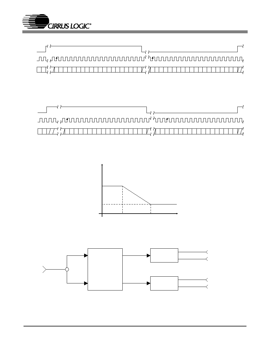
CS4382
DS514F1
37
LRCK
SCLK
Left Channel
Right Channel
SDINx
6
5
4
3
2
1
0
9
8
7
15 14 13 12 11 10
1
0
6
5
4
3
2
1
0
9
8
7
15 14 13 12 11 10
17 16
17 16
32 clocks
19 18
19 18
Figure 37. Format 4 - Right Justified 20-bit Data
LRCK
SCLK
Left Channel
Right Channel
SDINx
6
5
4
3
2
1
0
9
8
7
15 14 13 12 11 10
1
0
6
5
4
3
2
1
0
9
8
7
15 14 13 12 11 10
17 16
17 16
32 clocks
Figure 38. Format 5 - Right Justified 18-bit Data
Figure 39. De-Emphasis Curve
Gain
dB
-10dB
0dB
Frequency
T2 = 15 µs
T1=50 µs
F1
F2
3.183 kHz
10.61 kHz
SDINx
Channel
Pair x
Control
DAC
DAC
AOUTAx+
AOUTAx-
AOUTBx+
AOUTBx-
L
R
Figure 40. Channel Pair Routing Diagram (x = Channel Pair 1, 2, 3, or 4)
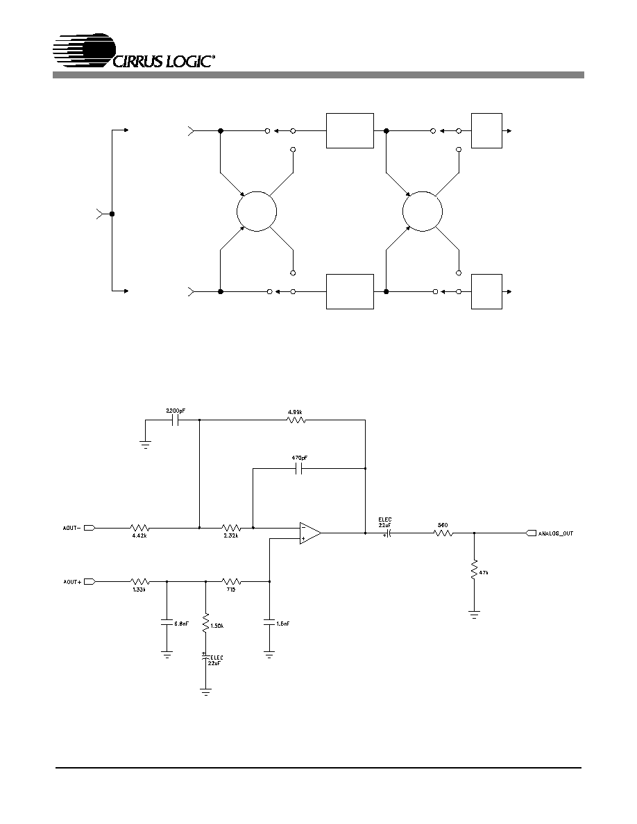
CS4382
38
DS514F1
A Channel
Volume
Control
Aout Ax
AoutBx
Left Chan
nel
Audio D
ata
Right Chan
nel
Audio D
ata
B Channel
Volume
Control
MUTE
MUTE
SDINx
Figure 41. ATAPI Block Diagram (x = channel pair 1, 2, 3, or 4)
Figure 42. Recommended Output Filter

CS4382
DS514F1
39
7. PARAMETER DEFINITIONS
Total Harmonic Distortion + Noise (THD+N)
The ratio of the rms value of the signal to the rms sum of all other spectral components over the specified
bandwidth (typically 10 Hz to 20 kHz), including distortion components. Expressed in decibels.
Dynamic Range
The ratio of the full scale rms value of the signal to the rms sum of all other spectral components over the
specified bandwidth. Dynamic range is a signal-to-noise measurement over the specified bandwidth
made with a -60 dBFS signal. 60 dB is then added to the resulting measurement to refer the measurement
to full scale. This technique ensures that the distortion components are below the noise level and do not
effect the measurement. This measurement technique has been accepted by the Audio Engineering So-
ciety, AES17-1991, and the Electronic Industries Association of Japan, EIAJ CP-307.
Interchannel Isolation
A measure of crosstalk between the left and right channels. Measured for each channel at the converter's
output with all zeros to the input under test and a full-scale signal applied to the other channel. Units in
decibels.
Interchannel Gain Mismatch
The gain difference between left and right channels. Units in decibels.
Gain Error
The deviation from the nominal full scale analog output for a full scale digital input.
Gain Drift
The change in gain value with temperature. Units in ppm/∞C.

CS4382
40
DS514F1
8. REFERENCES
1. "How to Achieve Optimum Performance from Delta-Sigma A/D & D/A Converters" by Steven Harris.
Paper presented at the 93rd Convention of the Audio Engineering Society, October 1992.
2. CDB4382 Evaluation Board Datasheet
3. "Design Notes for a 2-Pole Filter with Differential Input" by Steven Green. Cirrus Logic Application Note
AN48
4. "The I
2
C-Bus Specification: Version 2.0" Philips Semiconductors, December 1998.
http://www.semiconductors.philips.com

CS4382
DS514F1
41
9. PACKAGE DIMENSIONS
INCHES
MILLIMETERS
DIM
MIN
NOM
MAX
MIN
NOM
MAX
A
---
0.055
0.063
---
1.40
1.60
A1
0.002
0.004
0.006
0.05
0.10
0.15
B
0.007
0.009
0.011
0.17
0.22
0.27
D
0.343
0.354
0.366
8.70
9.0 BSC
9.30
D1
0.272
0.28
0.280
6.90
7.0 BSC
7.10
E
0.343
0.354
0.366
8.70
9.0 BSC
9.30
E1
0.272
0.28
0.280
6.90
7.0 BSC
7.10
e*
0.016
0.020
0.024
0.40
0.50 BSC
0.60
L
0.018
0.24
0.030
0.45
0.60
0.75
0.000∞
4∞
7.000∞
0.00∞
4∞
7.00∞
* Nominal pin pitch is 0.50 mm
Controlling dimension is mm.
JEDEC Designation: MS022
48L LQFP PACKAGE DRAWING
E1
E
D1
D
1
e
L
B
A1
A
CS4382
42
DS514F1
Table 9. Revision History
Contacting Cirrus Logic Support
For all product questions and inquiries contact a Cirrus Logic Sales Representative.
To find the one nearest to you go to www.cirrus.com
IMPORTANT NOTICE
Cirrus Logic, Inc. and its subsidiaries ("Cirrus") believe that the information contained in this document is accurate and reliable. However, the information is subject
to change without notice and is provided "AS IS" without warranty of any kind (express or implied). Customers are advised to obtain the latest version of relevant
information to verify, before placing orders, that information being relied on is current and complete. All products are sold subject to the terms and conditions of sale
supplied at the time of order acknowledgment, including those pertaining to warranty, patent infringement, and limitation of liability. No responsibility is assumed by
Cirrus for the use of this information, including use of this information as the basis for manufacture or sale of any items, or for infringement of patents or other rights
of third parties. This document is the property of Cirrus and by furnishing this information, Cirrus grants no license, express or implied under any patents, mask work
rights, copyrights, trademarks, trade secrets or other intellectual property rights. Cirrus owns the copyrights associated with the information contained herein and
gives consent for copies to be made of the information only for use within your organization with respect to Cirrus integrated circuits or other products of Cirrus. This
consent does not extend to other copying such as copying for general distribution, advertising or promotional purposes, or for creating any work for resale.
CERTAIN APPLICATIONS USING SEMICONDUCTOR PRODUCTS MAY INVOLVE POTENTIAL RISKS OF DEATH, PERSONAL INJURY, OR SEVERE PROP-
ERTY OR ENVIRONMENTAL DAMAGE ("CRITICAL APPLICATIONS"). CIRRUS PRODUCTS ARE NOT DESIGNED, AUTHORIZED OR WARRANTED FOR
USE IN AIRCRAFT SYSTEMS, MILITARY APPLICATIONS, PRODUCTS SURGICALLY IMPLANTED INTO THE BODY, LIFE SUPPORT PRODUCTS OR OTHER
CRITICAL APPLICATIONS (INCLUDING MEDICAL DEVICES, AIRCRAFT SYSTEMS OR COMPONENTS AND PERSONAL OR AUTOMOTIVE SAFETY OR SE-
CURITY DEVICES). INCLUSION OF CIRRUS PRODUCTS IN SUCH APPLICATIONS IS UNDERSTOOD TO BE FULLY AT THE CUSTOMER'S RISK AND CIR-
RUS DISCLAIMS AND MAKES NO WARRANTY, EXPRESS, STATUTORY OR IMPLIED, INCLUDING THE IMPLIED WARRANTIES OF MERCHANTABILITY
AND FITNESS FOR PARTICULAR PURPOSE, WITH REGARD TO ANY CIRRUS PRODUCT THAT IS USED IN SUCH A MANNER. IF THE CUSTOMER OR
CUSTOMER'S CUSTOMER USES OR PERMITS THE USE OF CIRRUS PRODUCTS IN CRITICAL APPLICATIONS, CUSTOMER AGREES, BY SUCH USE, TO
FULLY INDEMNIFY CIRRUS, ITS OFFICERS, DIRECTORS, EMPLOYEES, DISTRIBUTORS AND OTHER AGENTS FROM ANY AND ALL LIABILITY, INCLUD-
ING ATTORNEYS' FEES AND COSTS, THAT MAY RESULT FROM OR ARISE IN CONNECTION WITH THESE USES.
Cirrus Logic, Cirrus, and the Cirrus Logic logo designs are trademarks of Cirrus Logic, Inc. All other brand and product names in this document may be trademarks
or service marks of their respective owners.
I2C is a registered trademark of Philips Semiconductor. Purchase of I2C Components of Cirrus Logic, Inc., or one of its sublicensed Associated Companies conveys
a license under the Philips I2C Patent Rights to use those components in a standard I2C system.
SPI is a trademark of Motorola, Inc.
Release
Date
Changes
F1
NOV 2004
Removed -BQ ordering option
Corrected specifications for Full Scale Differential Output Voltage
Updated Table 2 on page 16
Updated Section 5.7 Using DSD mode
Updated legal text