 | –≠–ª–µ–∫—Ç—Ä–æ–Ω–Ω—ã–π –∫–æ–º–ø–æ–Ω–µ–Ω—Ç: CDB5460 | –°–∫–∞—á–∞—Ç—å:  PDF PDF  ZIP ZIP |
Document Outline
- CDB5460 Evaluation Board and Software
- Features
- General Description
- ORDERING INFORMATION
- TABLE OF CONTENTS
- PART I: HARDWARE
- Introduction
- Evaluation Board Overview
- Analog Section
- Figure 1. Analog Schematic Part 1
- Figure 2. Analog Schematic Part 2
- Table 1. Reference Selection
- Digital Section
- Figure 3. Digital Schematic Part 1
- Figure 4. Digital Schematic Part 2
- Power Supply Section
- Figure 5. Power Supply Schematic
- Using the Evaluation Board
- Table 3. Header, Jumper, DIP Switch Descriptions
- Table 4. DIP Switch S1 Setting
- PART II: SOFTWARE
- Installation Procedure
- Using the Software
- Figure 6. Start-Up Window
- Selecting and Testing a COM Port
- Register Access in the Setup Window
- Figure 7. Setup Window
- Refresh Screen Button:
- CS5460 Crystal Frequency:
- Configuration Register:
- Mask Register / Status Register:
- Cycle Count / Pulse Rate / Time Base Registers:
- Offset / Gain Registers:
- Performing Calibrations:
- Offset Calibrations:
- Gain Calibrations:
- Conversion Window
- Figure 8. Conversion Window
- Single Conversion Button:
- Continuous Conversions Button:
- Re-Initialize Serial Port Button:
- Standby / Sleep Mode Buttons:
- Power Up Button:
- Viewing Pulse Rate Output Data
- Figure 9. Pulse Rate Output Window
- Integration Period Box:
- Periods To Average Box:
- Start Button:
- Data Collection Window Overview
- Time Domain / FFT / Histogram Selector:
- Collect Button:
- Config Button:
- Output Button:
- Zoom Button:
- Channel Select Buttons:
- Config Window
- Number of Samples:
- Average:
- FFT Window:
- Histogram Bin Width:
- Pages to Collect:
- Data to Collect:
- Accept Button:
- Collecting Data Sets
- Retrieving Saved Data From a File
- Analyzing Data
- Histogram Information
- Figure 12. Histogram Analysis
- BIN:
- MAGNITUDE:
- MAXIMUM:
- MEAN:
- MINIMUM:
- STD. DEV.:
- VARIANCE:
- Frequency Domain Information
- Figure 11. FFT Analysis
- FREQUENCY:
- MAGNITUDE:
- S/D:
- S/N+D:
- SNR:
- S/PN:
- # of AVG:
- Time Domain Information
- Figure 10. Time Domain Analysis
- COUNT:
- MAGNITUDE:
- MAXIMUM:
- MINIMUM:
- PCB LAYOUT
- Figure 13. Silkscreen
- Figure 14. Circuit Side
- Figure 15. Solder Side

Preliminary Product Information
This document contains information for a new product.
Cirrus Logic reserves the right to modify this product without notice.
1
Copyright
©
Cirrus Logic, Inc. 1999
(All Rights Reserved)
Cirrus Logic, Inc.
Crystal Semiconductor Products Division
P.O. Box 17847, Austin, Texas 78760
(512) 445 7222 FAX: (512) 445 7581
http://www.crystal.com
VIN+
VIN-
IIN+
IIN-
CRYSTAL
4.096 MHz
REF
AGND
VOLTAGE
REFERENCE
AGND
CS5460
DGND
LEDs
EDIR
INT
SCLK
SDO
SDI
CS
80C51
Microcontroller
TEST
SWITCHES
CRYSTAL
20.0 MHz
RESET
CIRCUITRY
RS232
TRANS-
CEIVER
RS232
CONNECTOR
OUT
IN
EOUT
32k ◊ 8
SRAM
VD+
Vu+
VA-
VA+
VREF
CDB5460
CDB5460 Evaluation Board and Software
Features
l
Direct Shunt Sensor and Current
Transformer Interface
l
RS-232 Serial Communication with PC
l
On-board 80C51 Microcontroller
l
On-board Voltage Reference
l
Lab Windows/CVI
TM
Evaluation Software
- Register Setup & Chip Control
- FFT Analysis
- Time Domain Analysis
- Noise Histogram Analysis
l
On-board Data SRAM
l
Integrated RS-232 Test Mode
General Description
The CDB5460 is an inexpensive tool designed to evalu-
ate the functionality and performance of the CS5460.
The CS5460 Data Sheet is required in conjunction with
the CDB5460 evaluation board.
The evaluation board includes an LT1019 voltage refer-
ence, an 80C51 microcontroller, an RS232 transceiver,
and firmware. The 8051 controls the serial communica-
tion between the evaluation board and the PC via the
firmware, enabling quick and easy access to all of the
CS5460's registers and functions.
The CDB5460 includes software for Data Capture, Time
Domain Analysis, Histogram Analysis, and Frequency
Domain Analysis.
ORDERING INFORMATION
CDB5460 Evaluation Board
MAR `99
DS279DB1

CDB5460
2
DS279DB1
TABLE OF CONTENTS
PART I: HARDWARE .......................................................................................... 3
Introduction ................................................................................................. 3
Evaluation Board Overview ........................................................................ 3
Analog Section ..................................................................................... 3
Digital Section ...................................................................................... 3
Power Supply Section .......................................................................... 9
Using the Evaluation Board ........................................................................ 9
PART II: SOFTWARE ........................................................................................ 10
Installation Procedure ............................................................................... 10
Using the Software ................................................................................... 10
Selecting and Testing a COM Port ........................................................... 11
Register Access in the Setup Window ...................................................... 11
Conversion Window .................................................................................. 12
Viewing Pulse Rate Output Data .............................................................. 13
Data Collection Window Overview ............................................................ 13
Config Window .......................................................................................... 14
Collecting Data Sets ................................................................................. 14
Retrieving Saved Data From a File ........................................................... 15
Analyzing Data .......................................................................................... 15
Histogram Information .............................................................................. 15
Frequency Domain Information ................................................................ 15
Time Domain Information ......................................................................... 16
PCB LAYOUT .................................................................................................... 20
Contacting Cirrus Logic Support
For a complete listing of Direct Sales, Distributor, and Sales Representative contacts, visit the Cirrus Logic web site at:
http://www.cirrus.com/corporate/contacts/
IBM, AT and PS/2 are trademarks of International Business Machines Corporation.
Windows is a trademark of Microsoft Corporation.
Lab Windows and CVI are trademarks of National Instruments.
SPI
TM
is a trademark of Motorola.
Microwire
TM
is a trademark of National Semiconductor.
Preliminary product information describes products which are in production, but for which full characterization data is not yet available. Advance product infor-
mation describes products which are in development and subject to development changes. Cirrus Logic, Inc. has made best efforts to ensure that the information
contained in this document is accurate and reliable. However, the information is subject to change without notice and is provided "AS IS" without warranty of
any kind (express or implied). No responsibility is assumed by Cirrus Logic, Inc. for the use of this information, nor for infringements of patents or other rights
of third parties. This document is the property of Cirrus Logic, Inc. and implies no license under patents, copyrights, trademarks, or trade secrets. No part of
this publication may be copied, reproduced, stored in a retrieval system, or transmitted, in any form or by any means (electronic, mechanical, photographic, or
otherwise) without the prior written consent of Cirrus Logic, Inc. Items from any Cirrus Logic website or disk may be printed for use by the user. However, no
part of the printout or electronic files may be copied, reproduced, stored in a retrieval system, or transmitted, in any form or by any means (electronic, mechanical,
photographic, or otherwise) without the prior written consent of Cirrus Logic, Inc.Furthermore, no part of this publication may be used as a basis for manufacture
or sale of any items without the prior written consent of Cirrus Logic, Inc. The names of products of Cirrus Logic, Inc. or other vendors and suppliers appearing
in this document may be trademarks or service marks of their respective owners which may be registered in some jurisdictions. A list of Cirrus Logic, Inc. trade-
marks and service marks can be found at http://www.cirrus.com.

CDB5460
DS279DB1
3
PART I: HARDWARE
Introduction
The CDB5460 evaluation board provides a quick
means of evaluating the CS5460 Analog-to-Digital
Converters (ADCs) and Computational Unit. The
CDB5460 evaluation board's analog section oper-
ates from either a single +5 V or dual ±2.5 V power
supply. The evaluation board interfaces the
CS5460 to an IBM
TM
compatible PC via an RS-
232 interface. To accomplish this, the board comes
equipped with an 80C51 microcontroller and a 9-
pin RS-232 cable which physically interfaces the
evaluation board to the PC. Additionally, analysis
software provides easy access to the internal regis-
ters of the CS5460, and provides a means to display
the performance in the time domain or frequency
domain.
Evaluation Board Overview
The board is partitioned into two main sections: an-
alog and digital. The analog section consists of the
CS5460 and a precision voltage reference. The dig-
ital section consists of the 80C51 microcontroller,
32 Kilobytes of SRAM, the hardware test switches,
the reset circuitry, and the RS-232 interface. The
board also has a user friendly power supply con-
nection.
Analog Section
The CS5460 is designed to accurately measure and
calculate: Energy, Instantaneous Power, I
RMS
, and
V
RMS
while operating from a 4.096 MHz crystal.
As shown in Figure 1 there are four BNC connec-
tors (J9, J10, J11, J12) provided for converter input
connections. A Shunt Sensor or Current Trans-
former can be connected to the converter's current
inputs via J10 (IIN+) and J9 (IIN-). A voltage di-
vider can be connected to the converter's voltage
input via J12 (VIN+) and (J11) (VIN-). Note, a
simple RC network filters the sensor's output to re-
duce any interference picked up by the input leads.
The 3 dB corner of the filter is approximately 50K
Hz differential and common mode.
The evaluation board provides three voltage refer-
ence options, on-chip, on-board and external, as
shown in Figure 2. Table 1 illustrates the options
available. With HDR4's jumpers in position RE-
FOUT, the on-chip reference provides 2.5 volts.
With HDR4's jumpers in position LT1019, the
LT1019 provides 2.5 volts (the LT1019 was chosen
for its low drift, typically 5ppm/∞C). By setting
HDR4's jumpers to position REF+, the user can
supply an external voltage reference to J2's REF+
and VA- inputs. Application Note 4 on the web
(http://www.cirrus.com/products//pubs.html) de-
tails various voltage references.
The CS5460 serial interfaces are SPI
TM
and Mi-
crowire
TM
compatible. The interface control lines
(CS, SDI, SDO, and SCLK) are connected to the
80C51 microcontroller via port one. To interface an
external microcontroller, these control lines are
also connected to HDR6 (Header 6). However to
accomplish this, the evaluation board must be mod-
ified in one of three ways: 1) cut the interface con-
trol traces going to the microcontroller, 2) remove
resistors R4, R7, R8, and R13, or 3) remove the mi-
crocontroller.
Digital Section
Figures 3 and 4 illustrate the schematic of the digi-
tal section. It contains the microcontroller, test
Reference
Description
HDR4
LT1019
Selects on board
LT1019 Reference
(5ppm/
∞C)
REF+
Selects external
reference
REFOUT
Selects the reference
supplied by CS5460
Table 1. Reference Selection
O O LT1019
O O REF+
O O REFOUT
O O LT1019
O O REF+
O O REFOUT
O O LT1019
O O REF+
O O REFOUT

CDB
5460
4
DS2
79DB
1
DGND
CPUCLK
/EOUT
/EDIR
/INT
XOUT
COG
C39
10PF
AGND
R28
15K
VIN+
IIN+
IIN-
AGND
AGND
TP156
VREFIN
TP157
TP154
VREFOUT
TP155
TP152
VIN-
TP153
TP150
TP151
TP148
TP149
TP146
/CS
TP147
TP144
SDO
TP145
TP142
TP143
TP140
TP141
TP138
TP139
TP136
TP137
TP134
TP130
TP131
TP129
TP127
TP124
TP125
TP122
TP123
TP120
/RESET
TP121
TP118
/INT
TP119
TP116
/EOUT
TP117
TP114
/EDIR
TP115
TP112
SDI
TP113
TP110
XIN
TP111
COG
4700PF
C3
0.1%
301
R25
TP39
4
3
2
1
HDR8
HDR2X2
AGND
1
2
3
4
HDR9
HDR2X2
0.1%
301
R26
AGND
AGND
R18
301
0.1%
TP35
4
3
2
1
HDR2X2
HDR2
AGND
1
2
3
4
HDR2X2
HDR1
TP34
R17
301
0.1%
.1UF
C14
COG
C2
4700PF
AGND
TP40
TP133
VIN+
VIN-
COG
C32
.01UF
COG
C33
.01UF
COG
.01UF
C34
AGND
TP132
TP126
TP128
TP135
XOUT
COG
C35
.01UF
CPUCLK
IIN-
PFMON
IIN+
10UF
C29
PFMON
VA+
4.0960MHZ
Y2
COG
C38
10PF
22
21
20
19
18
17
16
15
14
13
12
11
10
9
8
7
6
5
4
3
2
1
HDR11X2
HDR6
/CS
SDI
SDO
SCLK
XTAL1
10K
R19
SCLK
JP2
C15
.1UF
C30
10UF
D+
VA+
A-
DCLK
/RESET
XIN
SDI
/EDIR
/EOUT
/INT
/RESET
NC
PFMON
IIN+
IIN-
VA+
AGND
VREFIN
VREFOUT
VIN-
VIN+
NC
/CS
SDO
SCLK
DGND
VD+
CPUCLK
XOUT
24
23
22
21
20
19
18
17
16
15
14
13
12
11
10
9
8
7
6
5
4
3
2
1
CS5460_EP
U3
J12
BNC_RA
BNC_RA
J10
J9
BNC_RA
J11
BNC_RA
AGND
4
3
2
1
HDR2X2
HDR10
DGND
DGND
DGND
DGND
XIN
Figure 1. Analog Schematic Part 1

CDB
5460
DS
2
79D
B1
5
DGND
DGND
DGND
DGND
VDDD
VREFOUT
VREFIN
R21
301
0.1%
.1UF
C20
GND
TEMP
HTR
TRIM
OUT
IN
6
5
7
3
4
2
LT1019CN8_2P5
U4
C16
.1UF
6
5
4
3
2
1
HDR3X2
HDR4
REF+
2
1
TERM_BLOCK
J2
DGND
SDO
/INT
/EDIR
/EOUT
2Y4
2Y3
2Y2
2Y1
1Y4
1Y3
1Y2
1Y1
GND
VCC
2A4
2A3
2A2
2A1
2/G
1A4
1A3
1A2
1A1
1/G
20
19
18
17
16
15
14
13
12
11
10
9
8
7
6
5
4
3
2
1
SN74HCT244N
U8
XTAL1
USDO
UINT
UEDIR
UEOUT
DGND
JP1
UXTAL1
A-
A-
R30
10K
R31
10K
A-
Y8
Y7
Y6
Y5
Y4
Y3
Y2
Y1
GND
VCC
A8
A7
A6
A5
A4
A3
A2
A1
/G2
/G1
20
19
18
17
16
15
14
13
12
11
10
9
8
7
6
5
4
3
2
1
TC74VHC541FW
U9
.1UF
C41
UCS
USDI
USCLK
UDCLK
/CS
SDI
SCLK
DCLK
DGND
C40
.1UF
C1
.1UF
A-
A-
A-
A-
D+
10K
R12
D+
URESET
/RESET
49.9
R24
VA+
A-
.1UF
C44
Figure 2. Analog Schematic Part 2

CDB
5460
6
DS2
79DB
1
ALE
TP8
TP14
TP22
TP3
TP2
TP1
TP69
5.11K
R11
1N4148
D4
DGND
C7
47UF
DGND
COG
33PF
C24
COG
33PF
C23
R9
750K
.1UF
C18
DGND
DGND
S2
SW_B3W_1100
R10
5.11K
TP30
TP31
TP32
TP33
TP10
TP11
TO RS-232
FROM RS-232
VDDD
RESET
VDDD
4
3
2
1
HDR2X2
HDR7
C19
.1UF
DGND
GND
VCC
3
7
14
2
1
SN74HC00N
U2
DGND
TP9
OPEN
1
2
3
S1
SW_DIP_3
BYPASS CAP
DGND
P0.4
P2.0
P2.1
P2.2
TP4
TP5
TP6
TP7
TP43
TP42
TP16
TP17
P2.3
P2.4
P2.5
P2.6
P2.7
TP25
TP26
TP27
TP28
TP29
TP23
TP24
TP15
TP38
TP18
TP19
TP20
TP21
P0.3
P0.5
P0.6
P0.7
P0.0
P0.1
P0.2
Y1
20.000 MHZ
JP4
P3.2
P3.6
P3.7
UXTAL1
DGND
C17
.1UF
DGND
DGND
VDDD
P3.7/\RD
P3.6/\WR
P3.5/T1
P3.4/T0
P3.3/\INT1
P3.2/\INT0
P3.1/TXD
P3.0/RXD
PORT1
1.7
1.0
A
PORT2
P2.7
P2.0
AD
PORT0
P0.7
P0.0
PROG
ALE
PSEN
RST
EA
XTAL2
XTAL1
#
8-BIT MICRO
8751
29
30
39
38
37
36
35
34
33
32
21
22
23
24
25
26
27
28
10
11
12
13
14
15
16
17
8
7
6
5
4
3
2
1
9
31
18
19
UM1
8751-8
8
7
6
5
4
3
2
1
LED_555_5003
D2
R4
200
R8
200
200
R13
UCS
USDI
USDO
USCLK
UDCLK
R16
200
200
R1
R2
200
R3
200
UINT
UEDIR
UEOUT
R7
200
R29
200
URESET
NRST
Figure 3. Digital Schematic Part 1

CDB
5460
DS
2
79D
B1
7
P3.6
P2.5
P2.0
P2.1
P2.3
P3.7
P2.2
P0.7
P0.6
P0.5
P0.4
P0.3
P0.2
P0.1
P0.0
A0
A1
A2
A3
A4
A5
A6
P2.4
A7
VDDD
P2.6
VDDD
DGND
P0.7
12
13
11
SN74HC00N
U2
C2+
GND
C2-
VSS
RX1
TX1
RX2
TX2
RX3
TX3
C1+
VCC
C1-
VDD
DO1
DI1
DO2
DI2
DO3
DI3
20
19
18
17
16
15
14
13
12
11
10
9
8
7
6
5
4
3
2
1
U1
MC145407P
C26
10UF
TO-PC
FROM-PC
TP13
C25
10UF
C28
10UF
9
8
7
6
5
4
3
2
1
DE9F_RA
J8
DGND
VDDD
TP71
TP72
DGND
10UF
C27
TP12
R14
10K
4
5
6
SN74HC00N
U2
P2.6
9
10
8
U2
SN74HC00N
P0.6
P0.5
P0.4
P0.3
P0.2
P0.1
P0.0
ALE
DGND
A0
A1
A2
A3
A4
A5
A6
A7
CSUSB
P2.7
DGND
.1UF
C42
.1UF
C43
/OC
C
1D
2D
3D
4D
5D
6D
6Q
5Q
4Q
3Q
2Q
1Q
VCC
GND
7D
8D
7Q
8Q
2
5
6
9
12
15
16
19
20
10
18
17
14
13
8
7
4
3
11
1
SN74HC373N
U5
DGND
DGND
A14
A0
A1
A2
A3
A4
A5
A6
A7
A12
A8
A9
A10
A11
A13
DQ0
DQ1
DQ2
VSS
VCC
/W
/G
/E
DQ3
DQ4
DQ5
DQ6
DQ7
28
27
26
25
24
23
22
21
20
19
18
17
16
15
14
13
12
11
10
9
8
7
6
5
4
3
2
1
MCM6206DP20
U6
Figure 4. Digital Schematic Part 2

CDB
5460
8
DS2
79DB
1
AGND
CON_BANANA
J6
VA+
VD+
VA-
CON_BANANA
J13
.1UF
C21
P6KE6V8P
Z4
C11
47UF
DGND
DGND
DGND
C8
47UF
P6KE6V8P
Z3
AGND
C5
47UF
J3
CON_BANANA
Z2
P6KE6V8P
47UF
C6
.1UF
C12
.1UF
C13
CON_BANANA
J5
AGND
.1UF
C10
DGND
DGND
AGND
6
5
4
3
2
1
HDR3X2
HDR3
AGND
AGND
AGND
Z1
P6KE6V8P
A-
DGND
10
R15
FERRITE_BEAD
L2
CON_BANANA
J4
Vu+
CON_BANANA
J14
8
7
6
5
4
3
2
1
HDR4X2
HDR5
VDDD
D+
DGND
AGND
AGND
VA+
Figure 5. Power Supply Schematic

CDB5460
DS279DB1
9
switches, a Motorola MC145407 interface chip,
and 32K bytes of SRAM. The test switches aid in
debugging communication problems between the
CDB5460 and the PC. The microcontroller derives
its clock from an 20.0 MHz crystal. From this, the
controller is configured to communicate via RS-
232 at 9600 baud, no parity, 8-bit data, and 1 stop
bit.
Power Supply Section
Figure 5 illustrates the power supply connections to
the evaluation board. The VA+ post supplies the
positive analog section of the evaluation board, the
LT1019 and the ADC. The VA- post supplies the
negative analog voltage circuitry. Note, this termi-
nal is grounded when powering the CDB5460 from
a single +5 Volt analog supply. The VD+ post sup-
plies the digital section of the ADC and level
shifter. The Vu+ post supplies the digital section of
the evaluation board, the 80C51, the reset circuitry,
and the RS-232 interface circuitry. Note, the
board's digital section supplied via Vu+ post, must
be +5Volts only. Table 2 shows the varies power
connections with the required jumper setting on
HDR3 and HDR5.
Using the Evaluation Board
The CS5460 is a highly integrated device, contain-
ing dual ADCs with a computational unit. The
CS5460 and CDB5460 data sheets should be read
thoroughly and understood before using the
CDB5460 evaluation board. The CS5460 contains
a programmable gain amplifier (PGA), two
modulators, two high rate filters, an on-chip refer-
ence, and power calculation engine to compute En-
ergy, V
RMS
, I
RMS
, and Instantaneous Power. The
PGA sets the input levels of the current channel at
either 30 mV
RMS
or 150 mV
RMS
(for VREFIN =
2.5 V). The on-chip reference can provide the nec-
essary 2.5 V reference. This output (VREFOUT),
along with a 10
µ
F capacitor, is used to supply the
VREFIN pin with 2.5 V. The
modulators and
high rate digital filter allows the user to measure in-
stantaneous voltage, current, and power at a output
word rate of 4000 Hz when a 4.096 MHz clock
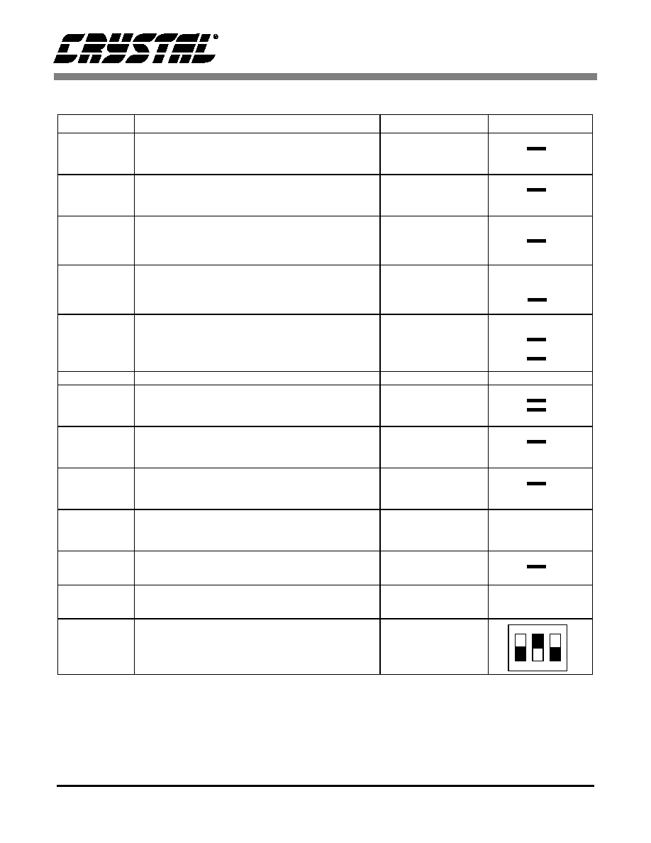
source is used. Table 3 describes the varies headers,
jumpers and DIP switches on the CDB5460 evalu-
ation board. DIP switch S1 is used to control the
80C51. Table 4 illustrates the varies setting of the
DIP Switch S1. Note, S1-3 is a no connect and not
used. The S1-1 switch should be set to the OPEN
position for normal operation. When testing the
RS-232 link in the PC software, close S1-1. The
Power Supplies
Power Post Connections
Jumpers
Analog
Digital
VA+
VA-
AGND DGND
VD+
Vu+
HDR5
HDR3
+5V
+5V
+5
NC
GND
GND
+5
NC
+5V
+3V
+5
NC
GND
GND
+3
+5
±
2.5V
+3V
+2.5
-2.5
NC
GND
+3
+5
Table 2. Power Supply Connections
O O VDDD
O O VDDD
O O V+
O O V+
Vu+
VD+
VD+
VA+
O O DGND
O O DGND
O O DGND
VA-
A-
AGND
O O VDDD
O O VDDD
O O V+
O O V+
Vu+
VD+
VD+
VA+
O O DGND
O O DGND
O O DGND
VA-
A-
AGND
O O VDDD
O O VDDD
O O V+
O O V+
Vu+
VD+
VD+
VA+
O O DGND
O O DGND
O O DGND
VA-
A-
AGND
CDB5460
10
DS279DB1
Name
Function Description
Default Setting
Default Jumpers
HDR1
Used to switch VIN+ on the CS5460 between J12
and AGND.
VIN+ Set to BNC J12
HDR2
Used to switch VIN- on the CS5460 between J11
and AGND.
VIN- Set to BNC J11
HDR3
Used to switch VA-, A-, and AGND to DGND.Refer
to Table 2
Negative Analog
Power Supply Set to
0 V
HDR4
Used to switch the VREFIN from external J2
header, to the on board LT1019 reference, or to the
on-chip reference VREFOUT. Refer to Table 1
VREFIN Set to on-
chip reference
VREFOUT
HDR5
Used to switch VU+, VD+, and VA+ to VDDD and/or
V+. Refer to Table 2
Digital Power Supply
Set to +5V
HDR6
Used to connect an external micro-controller.
Connected to 80C51
NC
HDR7
Used in conjunction with the self test modes to test
the UART/RS-232 communication link between the
microcontroller and a PC.
RS-232 Set to Normal
Mode
HDR8
Used to switch IIN+ on the CS5460 between J10
and AGND.
IIN+ Set to BNC J10
HDR9
Used to switch IIN- on the CS5460 between J9 and
AGND.
IIN- Set to BNC J11
HDR10
Used to switch XIN on the CS5460 to HDR6 when
an extrenal micro-controller is used.
XIN Set for on-board
4.096 MHz XTAL
JP2
Used to connect PFMON pin on the CS5460 to
monitor Power Supply VA+
PFMON Set Monitor
VA+
JP4
Used to connect the RESET Button to the CS5460
RESET Set not con-
nected to CS5460
S1
DIP switch to control 80C51
S1-1 is used to select RS-232 test mode
S1-2 is used to select crystal to 80C51
S1-1 Set Normal
S1-2 Set 20 MHz
Table 3. Header, Jumper, DIP Switch Descriptions
O O VIN+
O O AGND
O O VIN-
O O AGND
O O DGND
O O DGND
O O DGND
VA-
A-
AGND
O O LT1019
O O REF+
O O REFOUT
O O VDDD
O O VDDD
O O V+
O O V+
Vu+
VD+
VD+
VA+
O O
O O
HDR7
O O IIN+
O O AGND
O O IIN-
O O AGND
O O DGND
O O XIN
O O JP2
O O JP4
1
2
3
OPEN

CDB5460
DS279DB1
11
S1-2 switch selects the crystal source for the
80C51. There are two crystal options available,
11.059 MHz and 20 MHz. If S1-2 is OPEN the
11.059 MHz crystal is selected, and when S1-2 is
CLOSED the 20 MHz crystal is selected.
PART II: SOFTWARE
The evaluation board comes with software and an
RS-232 cable to link the evaluation board to the
PC. The evaluation software was developed with
Lab Windows/CVI
TM
, a software development
package from National Instruments. The software
was designed to run under Windows 95
TM
or later,
and requires about 3MB of hard drive space (2MB
for the CVI Run-Time Engine
TM
, and 1MB for the
evaluation software). After installing the software,
read the readme.txt file for any last minute updates
or changes. More sophisticated analysis software
can be developed by purchasing the development
package from National Instruments (512-794-
0100).
Installation Procedure
1) Turn on the PC, running Windows 95
TM
or
later.
2) Insert the Installation Diskette #1 into the PC.
3) Select the Run option from the Start menu.
4) At the prompt, type: A:\SETUP.EXE
<enter>.
5) The program will begin installation.
6) If it has not already been installed on the PC,
the user will be prompted to enter the direc-
tory in which to install the CVI Run-Time
Engine
TM
. The Run-Time Engine
TM
manages
executables created with Lab Win-
dows/CVI
TM
. If the default directory is
acceptable, select OK and the Run-Time
Engine
TM
will be installed there.
7) After the Run-Time Engine
TM
is installed, the
user is prompted to enter the directory in
which to install the CDB5460 software.
Select OK to accept the default directory.
8) Once the program is installed, it can be run by
double clicking on the Eval5460 icon, or
through the Start menu.
Note: The software is written to run with 640 x 480 res-
olution; however, it will work with 1024 x 768 resolution.
If the user interface seems to be a little small, the user
might consider setting the display settings to 640 x 480.
(640x480 was chosen to accommodate a variety of
computers).
Using the Software
Before launching the software, the user should set
up the CDB5460 evaluation board by using the cor-
rect jumper and DIP switch settings as described in
Part I, and connect it to an open COM port on the
PC using the RS-232 serial cable. Once the board is
powered on, the user can start the software pack-
age.
When the software is launched, the Start-Up win-
dow appears first (Figure 6). This window contains
information concerning the software's title, revi-
80C51 Mode
S1
80C51 is in Normal Operating Mode
S1-1 OPEN
S1-2 CLOSED 20 MHz Crystal
80C51 is in Normal Operation Mode
S1-1 OPEN
S1-2 OPEN 11.059 MHz Crystal
80C51 is in Test Mode
S1-1 CLOSED
S1-2 CLOSED 20 MHz Crystal
80C51 is in Test Mode
S1-1 CLOSED
S1-2 OPEN 11.059 MHz Crystal
Table 4. DIP Switch S1 Setting
1
2
3
OPEN
1
2
3
OPEN
1
2
3
OPEN
1
2
3
OPEN

CDB5460
12
DS279DB1
sion number, copyright date, etc. At the top of the
screen is a menu bar which displays user options.
The menu bar item Menu is initially disabled to
prevent conflicts with other serial communications
devices, such as the mouse or a modem. After se-
lecting a COM port, the Menu item will become
available.
Selecting and Testing a COM Port
Upon start-up, the user is prompted to select the se-
rial communications port which will interface to
the CDB5460 board. To select the COM port, pull
down the Setup menu option, and select either
COM1 or COM2 (the DISK option is used for pre-
viously saved files, and is discussed later). Testing
the COM port to verify communication between
the PC and the evaluation board is not necessary,
but can help to troubleshoot some problems. The
procedure for testing the communication link fol-
lows.
1) Pull down the Setup menu option again, and
select TEST RS-232.
2) When prompted, set DIP switch 1 (the left-
most DIP switch) to the closed position, reset
the board, and press OK to perform the test.
3) If the test passes, set DIP switch 1 to the open
position, and reset the board to return to nor-
mal operating mode.
4) If the test fails, check the serial port connec-
tions, power connections, jumpers, and DIP
switch settings on the board, and run the test
again from step 1.
Once the serial link is established between the PC
and the evaluation board, the user is ready to access
the internal registers of the CS5460, collect data,
and perform analysis on the collected data.
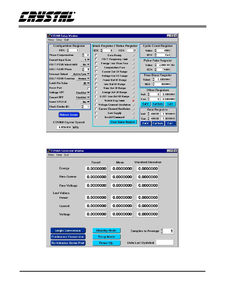
Register Access in the Setup Window
The Evaluation software provides access to the
CS5460's internal registers in the Setup Window
(Figure 7). The user can enter the Setup Window by
pulling down Menu and selecting Setup Window,
or by pressing F2 on the keyboard.
In the Setup Window, all of the CS5460's registers
are displayed in hexadecimal value, and also de-
coded to provide easier access. Refer to the
CS5460 data sheet for information on register func-
tionality and meanings.
Refresh Screen Button: The Refresh Screen but-
ton will update the contents of the screen by read-
ing all the register values from the part. This
usually takes a couple of seconds, but it is a good
idea to press the Refresh Screen button when enter-
ing the Setup Window, or after modifying any reg-
isters to reflect the current status of the part.
CS5460 Crystal Frequency: The CS5460 accepts
a wide range of crystal input frequencies, and can
therefore run at many different sample rates. The
crystal frequency being used on the CS5460 should
be entered in this box to provide accurate frequency
calculations in the FFT window. This will also help
the software decide which functions can be per-
formed reliably with the evaluation system.
Configuration Register: In the Configuration
Register box, the contents of the Configuration
Register can be modified by typing a hexadecimal
value in the HEX: box, or by changing any of the
values below the HEX: box to the desired settings.
Note: When changing the value of the reset bit to
`1' (RS, bit 7 in the Configuration Register), the
part will be reset, and all registers will return to
their default values. Press the Refresh Screen but-
ton after performing a reset to update the screen
with the new register values.
Note: Although the CDB5460 software allows the
user to modify any of the bits in the Configuration
Register, changing certain bits may cause the soft-
ware and board to behave erratically. For the eval-
uation system to function properly, the Interrupt
Output function should be set to the default Active
Low, and the Eout / Edir Function should be set to
the default Normal. This applies only to the

CDB5460
DS279DB1
13
CDB5460 evaluation system, and not to the
CS5460 chip itself.
Mask Register / Status Register: The Mask and
Status Registers are displayed in hexadecimal and
decoded in this box to show what each of the bits
means. The Mask Register can be modified by typ-
ing a value in the HEX: box, or by checking the ap-
propriate check boxes for the bits that are to be
masked. The Status Register cannot be directly
modified. It can only be reset by pressing the Clear
Status Register Button. The HEX: box for this reg-
ister, and the LEDs are display only. A LED that is
on means that the corresponding bit in the Status
Register is set (except the Invalid Command bit,
which is inverted).
Note: The value present in the Mask register may
be changed by the software during certain opera-
tions to provide correct functionality of the
CDB5460 board.
Cycle Count / Pulse Rate / Time Base Registers:
These three boxes display the values of the Cycle
Count, Pulse Rate, and Time Base Registers in both
hexadecimal and decimal format. All three regis-
ters can be modified by typing a value in the corre-
sponding Value: or HEX: box.
Offset / Gain Registers: In the Offset and Gain
Register boxes, the offset and gain registers for
both channels are displayed in hexadecimal and
decimal. These registers can all be modified direct-
ly by typing the desired value in the hexadecimal
display boxes.
Performing Calibrations: Offset and gain calibra-
tions can be performed on both the voltage and cur-
rent channels of the CS5460. Offset calibration
should be performed before gain calibration to en-
sure accurate results.
Offset Calibrations:
1) Ground the channel(s) you want to calibrate
directly at the channel header(s). HDR1 and
HDR2 for the voltage channel, and HDR8
and HDR9 for the current channel. The chan-
nel(s) could also be grounded directly at the
BNC connectors.
2) Press the corresponding Calibrate button (Cal
V, Cal I, or Cal Both) in the Offset Register
box.
3) The calibration value(s) will automatically
update when the calibration is completed.
Gain Calibrations:
1) Attach a full-scale calibration signal to the
BNC connector(s), and make sure the corre-
sponding channel headers (HDR1, HDR2,
HDR8, and HDR9) are set to the input posi-
tion.
2) Press the corresponding Calibrate button (Cal
V, Cal I, or Cal Both) in the Gain Register
box.
3) The calibration value(s) will automatically
update when the calibration is completed.
Conversion Window
The Conversion Window (Figure 8) allows the user
to see the results of single and continuous conver-
sions on all six data registers, perform data averag-
ing, utilize the power-saving modes of the CS5460,
and reset the CS5460's serial port. The Conversion
Window can be accessed by pulling down the
Menu option, and selecting Conversion Window,
or by pressing F3.
Single Conversion Button: On pressing this but-
ton, single conversions will be performed repeated-
ly until the user presses the Stop button. After each
conversion is complete, the Result data column will
update with the values present in each data register.
The Mean and Standard Deviation columns will
update every N cycles, where N is the number in
the Samples to Average box. Note: It can take
many collection cycles after pressing the Stop but-
ton before the data actually sops being collected.

CDB5460
14
DS279DB1
Continuous Conversions Button: This button
functions similarly to the Single Conversion but-
ton, except that continuous conversions are per-
formed instead. The data on the screen is updated
in the same fashion, and the Stop button terminates
this action. There are some speed limitations when
performing this function, and if any of these limita-
tions are exceeded, the user will be prompted to
change some settings before proceeding.
Re-Initialize Serial Port Button: When this but-
ton is pressed, the software will send the synchro-
nization sequence discussed in the CS5460 data
sheet to the part. This sequence brings the
CS5460's serial port back to a known state. It does
not reset any of the registers in the part.
Standby / Sleep Mode Buttons: When these but-
tons are pressed, the part will enter either Standby
or Sleep power saving modes. To return to normal
mode, use the Power Up button.
Power Up Button: This button is used to send the
Power Up/Halt command to the CS5460. The part
will return to normal operating mode and halt any
conversions that are being done at this time.
Viewing Pulse Rate Output Data
The CS5460 features a pulse-rate energy output.
The CDB5460 has the capability to demonstrate
the functionality of this output in the Pulse Rate
Output Window (Figure 9). The Pulse Rate Output
Window can be accessed by pressing the F4 key, or
by pulling down the Menu option, and selecting
Pulse Rate Window.
Integration Period Box: This box allows the user
to select the length of time which pulses will be col-
lected over.
Periods To Average Box: This box allows the user
to average a number of integration periods togeth-
er.
Start Button: When the Start button is pressed, the
CDB5460 will capture pulse rate data according to
the values in the Integration Period and Periods to
Average boxes. After each integration period, the
Pulse Count and Frequency columns will be updat-
ed. The Average Freq. and Standard Deviation col-
umns will only be updated after all of the
integrations have been collected. The software
stops collecting data when the user presses the Stop
button, or when the data collection is finished. Due
to some speed limitations of the on-board micro-
controller, some higher pulse rates cannot be accu-
rately collected. If the pulse rate is too high, a
warning message will appear.
Data Collection Window Overview
The Data Collection Window (Figures 10, 11, and
12) allows the user to collect sample sets of data
from the CS5460 and analyze them using time do-
main, FFT, and histogram plots. The Data Collec-
tion Window is accessible through the Menu
option, or by pressing F5.
Time Domain / FFT / Histogram Selector: This
menu selects the type of data processing to perform
on the collected data and display in the plot area.
Refer to the section on Analyzing Data for more in-
formation.
Collect Button: This button will collect data from
the part, to be analyzed in the plot area. See the sec-
tion on Collecting Data Sets for more information.
Config Button: This button will bring up the con-
figuration window, in which the user can modify
the data collection specifications. See the discus-
sion of the Config Window in this document.
Output Button: This button will bring up a win-
dow in which the user can output the data to a data
file for later use, print out a plot, or print out the en-
tire screen.
Note: When saving data, only the data channel be-
ing displayed on the plot will be saved to a file.
Zoom Button: This button allows the user to zoom
in on the plot by selecting two points in the plot ar-
ea. Press the Restore button to return to the normal

CDB5460
DS279DB1
15
data plot, or press the Zoom button again to zoom
in even further.
Channel Select Buttons: Depending on the num-
ber of channels of information that has been col-
lected, between 1 and 3 channel select buttons will
appear below the graph, allowing the user to
choose the appropriate channel for display. In the
Time Domain mode, an additional button labeled
"Overlay" will be present, to allow the user to dis-
play all of the channels on the same plot.
Config Window
The Config Window allows the user to set up the
data collection and analysis parameters.
Number of Samples: This box allows the user to
select the number of samples to collect, between 16
and 8192. Due to memory size on the CDB5460,
the maximum is 4096 samples when collecting two
channels, and 2048 samples when collecting three
channels.
Average: When doing FFT processing, this box
will determine the number of FFTs to average.
FFTs will be collected and averaged when the Col-
lect button is pressed.
FFT Window: This box allows the user to select
the type of windowing algorithm for FFT process-
ing. Windowing algorithms include the Blackman,
Blackman-Harris, Hanning, 5-term Hodie, and 7-
term Hodie. The 5-term Hodie and 7-term Hodie
are windowing algorithms developed at Crystal
Semiconductor.
Histogram Bin Width: This box allows for a vari-
able "bin width" when plotting histograms of the
collected data. Each vertical bar in the histogram
plot will contain the number of output codes con-
tained in this box. Increasing this number may al-
low the user to view histograms with larger input
ranges.
Pages to Collect: This box determines the number
of data "pages" that the microcontroller will collect
before sending data to the PC. Each page consists
of the number of samples collected, and only the
last page will be returned to the PC for processing.
This function is useful at higher sampling frequen-
cies to minimize board-level noise at the beginning
of the conversion set.
Data to Collect: These six check boxes allow the
user to select the data channels that will be collect-
ed and returned to the PC for processing. Up to
three channels can be selected at once. There are
some restrictions on the speed and number of sam-
ples to collect when selecting more than one chan-
nel. A warning message will appear on pressing the
Collect button in the Data Collection Window if
any speed limits appear to be exceeded, but the data
collection will still take place.
Accept Button: When this button is pressed, the
current settings will be saved, and the user will re-
turn to the Data Collection Window.
Collecting Data Sets
To collect a sample data set:
1) In the Data Collection Window, press the Con-
fig button to bring up the Configuration Win-
dow and view the current settings.
2) Select the appropriate settings from the avail-
able options (see the section on the Configu-
ration Window) and press the Accept button.
3) The Data Collection Window should still be
visible. Press the Collect button to begin col-
lecting data. A progress indicator bar will
appear at the bottom of the screen during the
data collection process.
4) Data is first collected from the CS5460 and
stored in SRAM, and then transferred from
the SRAM to the PC through the RS-232
serial cable. Depending on the value of the
Cycle Count Register and the number of sam-
ples being collected, this process may take a
long time. The process can be terminated by
pressing the Stop button, but if this is done,
the user should also press Reset on the
CDB5460 board.

CDB5460
16
DS279DB1
5) Once the data has been collected, it can be ana-
lyzed, printed, or saved to disk.
Retrieving Saved Data From a File
The CDB5460 software allows the user to save data
to a file, and retrieve it later when needed. To load
a previously saved file:
1) Pull down the Setup option and select Disk. A
file menu will appear.
2) Find the data file in the list and select it. Press
the Select button to return.
3) Go to the Data Collection Window, and press
the Collect button.
4) The data from the file should appear on the
screen. To select a different file, repeat the
procedure.
Analyzing Data
The evaluation software provides three types of
analysis tests - Time Domain, Frequency Domain,
and Histogram. The Time Domain analysis pro-
cesses acquired conversions to produce a plot of
Conversion Sample Number versus Magnitude.
The Frequency Domain analysis processes ac-
quired conversions to produce a magnitude versus
frequency plot using the Fast-Fourier transform
(results up to Fs/2 are calculated and plotted). Also,
statistical noise calculations are calculated and dis-
played. The Histogram analysis test processes ac-
quired conversions to produce a histogram plot.
Statistical noise calculations are also calculated and
displayed.
Histogram Information
The following is a description of the indicators asso-
ciated with Histogram Analysis. Histograms can be
plotted in the Data Collection Window by setting the
Time Domain / FFT / Histogram selector to Histo-
gram (Figure 12).
BIN: Displays the x-axis value of the cursor on the
Histogram.
MAGNITUDE: Displays the y-axis value of the
cursor on the Histogram.
MAXIMUM: Indicator for the maximum value of
the collected data set.
MEAN: Indicator for the mean of the data sample set.
MINIMUM: Indicator for the minimum value of
the collected data set.
STD. DEV.: Indicator for the Standard Deviation
of the collected data set.
VARIANCE: Indicates the Variance for the cur-
rent data set.
Frequency Domain Information
The following describe the indicators associated
with FFT (Fast Fourier Transform) Analysis. FFT
data can be plotted in the Data Collection Window
by setting the Time Domain / FFT / Histogram selec-
tor to FFT (Figure 11).
FREQUENCY: Displays the x-axis value of the
cursor on the FFT display.
MAGNITUDE: Displays the y-axis value of the
cursor on the FFT display.
S/D: Indicator for the Signal-to-Distortion Ratio, 4
harmonics are used in the calculations (decibels).
S/N+D: Indicator for the Signal-to-Noise + Distor-
tion Ratio (decibels).
SNR: Indicator for the Signal-to-Noise Ratio, first
4 harmonics are not included (decibels).
S/PN: Indicator for the Signal-to-Peak Noise Ratio
(decibels).
# of AVG: Displays the number of FFT's averaged
in the current display.
Time Domain Information
The following controls and indicators are associat-
ed with Time Domain Analysis. Time domain data
can be plotted in the Data Collection Window by set-
ting the Time Domain / FFT / Histogram selector to
Time Domain (Figure 10).

CDB5460
DS279DB1
17
COUNT: Displays current x-position of the cursor
on the time domain display.
MAGNITUDE: Displays current y-position of the
cursor on the time domain display.
MAXIMUM: Indicator for the maximum value of
the collected data set.
MINIMUM: Indicator for the minimum value of
the collected data set.
Figure 6. Start-Up Window
CDB5460
18
DS279DB1
Figure 7. Setup Window
Figure 8. Conversion Window

CDB5460
DS279DB1
19
Figure 9. Pulse Rate Output Window
Figure 10. Time Domain Analysis

CDB5460
20
DS279DB1
Figure 11. FFT Analysis
Figure 12. Histogram Analysis

CDB5460
DS279DB1
21
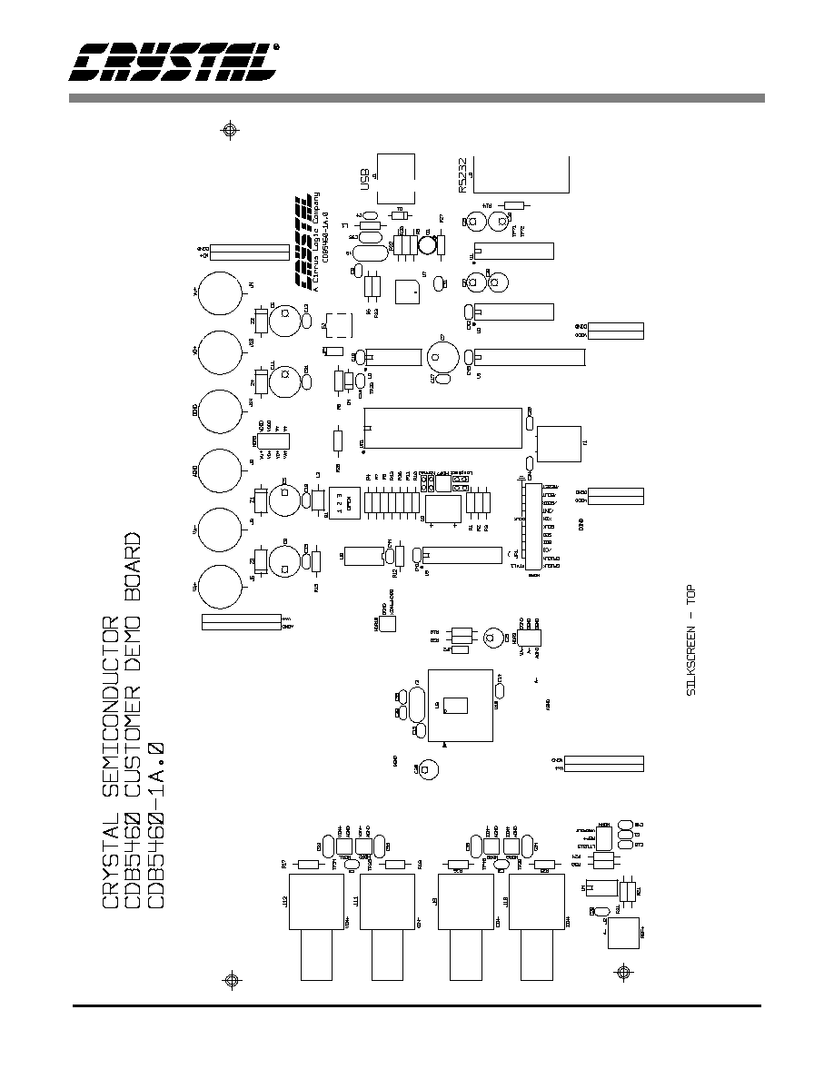
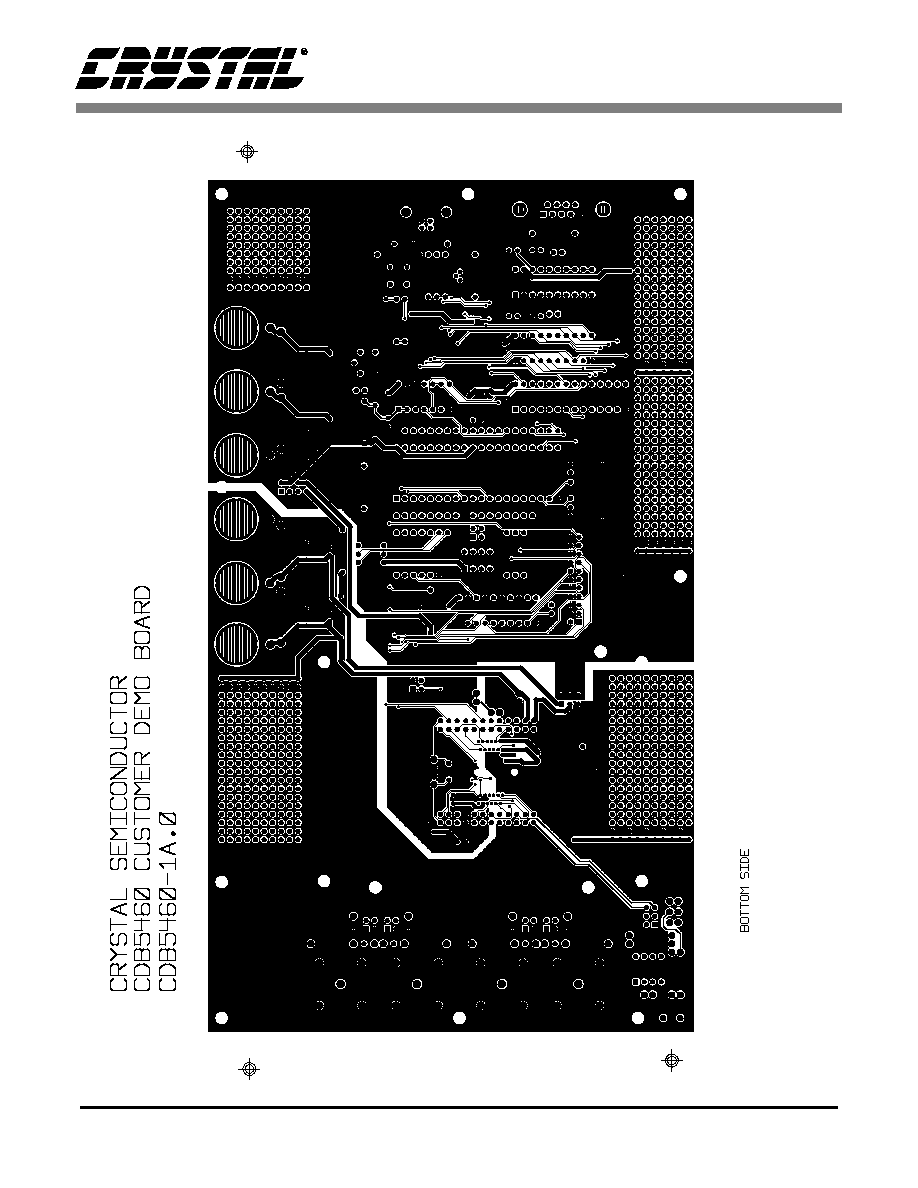
PCB LAYOUT
The CS5460 should be placed entirely over an ana-
log ground plane with both the VA- and DGND
pins of the device connected to the analog plane.
Place the analog-digital plane split immediately ad-
jacent to the digital portion of the chip. Figures 14
and 15 show the layout of the CDB5460.
Note: See Applications Note 18 for more detailed layout
guidelines. Before layout, please call for our Free Sche-
matic Review Service.
CDB
5460
22
DS2
79DB
1
Figure 13. Silkscreen

CDB
5460
DS
2
79D
B1
23
Figure 14. Circuit Side
CDB
5460
24
DS2
79DB
1
Figure 15. Solder Side

∑ Notes ∑
