 | –≠–ª–µ–∫—Ç—Ä–æ–Ω–Ω—ã–π –∫–æ–º–ø–æ–Ω–µ–Ω—Ç: CL-PS7110 | –°–∫–∞—á–∞—Ç—å:  PDF PDF  ZIP ZIP |
CL-PS7110
Data Book
May 1997
Version 1.5
OVERVIEW
FEATURES
s
Ultra low power
-- Designed for applications that require long battery life
while using standard AA/AAA batteries
-- Average 20 mA in normal operation (everything on)
-- Average 5 mA in idle mode (clock to the CPU stopped,
everything else running)
--
Average 3
µ
A in standby mode (realtime clock on and
everything else stopped)
s
Performance matching 33-MHz Intel
Æ
'486-based
PC
--
15 Vax
TM
-MIPS (Dhrystone
Æ
) at 18 MHz
s
ARM710A microprocessor
-- ARM7 CPU
-- 8 Kbytes of four-way set-associative cache
-- MMU with 64-entry TLB (transition look-aside buffer)
-- Little endian
s
DRAM controller
-- Connects up to four banks of DRAM, with each bank
being 32 bits wide and up to 256 Mbytes in size
The CL-PS7110 is designed for ultra-low-power
applications such as organizers/PDAs, two-way
pagers, smart phones, and hand-held internet
browsers. The device's core-logic functionality is
built around an ARM710A microprocessor with 8
Kbytes of four-way set-associative unified cache.
At 18.432 MHz (for 3-V operation), the CL-PS7110
delivers nearly 15 Vax-MIPS of performance (based
on Dhrystone
Æ
benchmark) -- roughly the same
Functional Block Diagram
32.768-kHz
OSCILLATOR
18.432-MHz
PLL
INTERRUPT
CONTROLLER
POWER
MANAGEMENT
SYNCHRONOUS
SERIAL I/O
STATE
CONTROL
DRAM
CONTROLLER
LCD
CONTROLLER
ARM7
µ
P CORE
8-KBYTE
CACHE
MMU
COUNTERS
(2)
RTC
CODEC
INTERFACE
ARM710A
INTERNAL DATA BUS
PSU
CONTROL
3.6864 MHz
32.786 kHz
EINT[1≠3],
FIQ
BATOK, EXTPWR
PWRFL, BATCHG
PORTS A B C D -- 8-BIT
PORT E -- 4-BIT
KEYBOARD COLUMN
DRIVES (0≠7)
BUZZER DRIVE
DC TO DC
CLK, SYNC, IN,
OUT, SMPCLK
CLK, SYNC IN,
OUT
UART
MUX
ROM/EXPANSION
CONTROL
IRDA
D0≠D31
POR, RUN,
RESET,
WAKEUP
EXPCLK, WORD,
CD[0≠7], EXPRDY,
WRITE
MOE, MWE
RAS[0≠3], CAS[0≠3]
A[0≠27],
DRA[0≠12]
LCD DRIVE
LED AND PHOTO-
DIODE
RS232 INTERFACE
INTERNAL
GPIO
ADDRESS BUS
(cont.)
Low-Power
System-on-a-Chip
(cont.)

DATA BOOK v1.5
May 1997
2
CL-PS7110
Low-Power System-on-a-Chip
OVERVIEW
(cont.)
system. The system can have an 8-bit-wide boot
option to optimize memory size.
The DRAM interface allows direct connection of up
to 4 banks of DRAM, each bank containing up to
256 Mbytes. To assure the lowest possible power
consumption, the CL-PS7110 supports self-refresh
DRAMs, which are placed a low-power state by the
device when it enters its low-power standby mode.
Serial Interface
For RS232 serial communications, the CL-PS7110
includes a UART with two 16-byte FIFOs for receive
and transmit data. The UART supports bit rates of
u p t o 1 1 5 . 2 k b p s . A n I r DA S I R p r o t o c o l
encoder/decoder can be optionally switched into the
Rx/Tx signals to/from the UART to enable these sig-
nals to drive an infrared communication interface
directly.
A full-duplex codec interface allows direct connec-
tion of a standard codec chip to the CL-PS7110,
allowing storage and playback of sound.
s
ROM/SRAM/flash memory control
-- Decodes eight separate memory segments of 256
Mbytes
-- Each segment can be configured as 8, 16, or 32 bits
wide and support page-mode access
-- Programmable access time for conventional
SRAM/ROM/flash memory
-- Expansion device can also be a PC Card (PCMCIA)
controller
s
Codec interface
-- Provides all necessary clocks and timing pulses and
performs serialization of the data stream (or vice versa)
to or from standard telephony codecs
-- Data transfer at 64 kbps
s
Synchronous serial interface
-- Supports SPI
Æ
1
or Microwire
Æ
2
-compatible interface
s
36-bit general-purpose I/O
-- Four 8-bit and one 4-bit GPIO port
-- Supports scanning keyboard matrix
1
SPI is a registered trademark of Motorola
Æ
.
2
Microwire is a registered trademark of National Semicon-
ductor
Æ
.
s
16C550-style UART
-- Supports bit rates up to 115.2 kbps
-- Contains two 16-byte FIFOs for Tx and Rx
-- Supports modem control signals
s
SIR (slow (9600≠115.2 kbps) infrared) encoder
-- IrDA (Infrared Data Association) SIR protocol encoder
can be optionally switched into Tx and Rx signals of the
UART up to 115 kbps
s
DC-to-DC converter interface
-- Provides two 96-kHz clock outputs, whose duty ratio are
programmable (from 1-in-16 to 15-in-16)
s
LCD controller
-- Interfaces directly to a single-scan panel monochrome
LCD
-- Panel size is programmable and is any width (line length)
from 16 to 1024 pixels in 16-pixel increments
-- Video frame size programmable up to 128 Kbytes
-- Bits per pixel programmable from 1, 2, or 4
-- Two 32-bit palette registers to support 4-, 2-, or 1-bit pixel
values for mapping to any of the 16 grayscale values
s
Two timer counters
s
Realtime clock (32-bit)
level of performance offered by a 33-MHz Intel
Æ
'486-
based PC.
As shown in the system block diagram, simply adding
desired memory and peripherals to the highly inte-
grated CL-PS7110 completes a hand-held orga-
nizer/PDA system board. All the interface logic is
integrated on-chip.
The CL-PS7110 is packaged in a 208-pin VQFP
package, with a body size of 28-mm square, lead
pitch of 0.5 mm, and thickness of 1.4 mm.
Memory Interface
There are two main external memory interfaces and
a DMA controller that fetches video display data for
the LCD controller from main DRAM memory.
The SRAM/ROM-style interface has programmable
wait state timings and includes burst-mode capability,
with eight chip selects decoding eight 256-Mbyte
sections of addressable space. For maximum flexibil-
ity, each bank can be specified to be 8, 16 or 32 bits
wide to enable the use of low-cost memory in a 32-bit
FEATURES
(cont.)

May 1997
3
DATA BOOK v1.5
CL-PS7110
Low-Power System-on-a-Chip
A CL-PS7110≠Based System
LCD MODULE
KEYBOARD
BATTERY
DC-TO-DC
CONVERTERS
ADC
DIGITIZER
IR LED AND
PHOTODIODE
RS232
TRANSEIVER
CODEC
ADDITIONAL I/O
PCMCIA
BUFFERS
PCMCIA
SOCKET
WRITE
CS[4]
CS[5]
EXPRDY
EXPCLK
WORD
DD[3:0]
CL1
CL2
FM
M
D[31:0]
A[27:0]
COL[7:0]
PA[7:0]
DC
INPUT
NMOE
NMWE
NRAS[3]
NRAS[2]
NRAS[1]
NRAS[0]
NCAS[0]
NCAS[1]
NCAS[2]
NCAS[3]
PB[7:0]
PC[7:0]
PD[7:0]
PE[3:0]
NPOR
NPWRFL
BATOK
NEXTPWR
NBATCHG
RUN
WAKEUP
NCS[0]
NCS[1]
DRIVE[1:0]
FB[1:0]
CL-PS7110
ADCCLK
NADCCS
ADCOUT
ADCIN
SMPCLK
LEDDRV
PHDIN
RXD
TXD
DSR
CTS
DCD
PCMCK
PCMSYNC
PCMOUT
PCMIN
CS[6]
CS[7]
NCS[2]
NCS[3]
◊
16
DRAM
◊
16
DRAM
◊
16
DRAM
◊
16
DRAM
◊
16
FLASH
◊
16
FLASH
◊
16
ROM
EXTERNAL MEMORY
MAPPED EXPANSION
BUFFERS
BUFFERS
AND
LATCHES
◊
16
ROM
◊
16
DRAM
◊
16
DRAM
◊
16
DRAM
◊
16
DRAM
POWER
SUPPLY UNIT
AND
COMPARATORS
A separate synchronous serial interface sup-
ports two industry-standard protocols (SPI
Æ
and Microwire
Æ
) for interfacing to standard
devices such as an ADC, allowing for peripheral
expansion such as the use of a digitizer pen.
Power Management
The CL-PS7110 is designed for low-power
operation. There are three basic power states:
q
Standby --
This state is equivalent to the com-
puter being switched off (no display), and the
main oscillator is shut down. Only the realtime
clock is running.
q
Idle --
In this state,
the device is functioning and
all oscillators are running, but the processor
clock is halted while waiting for an event such as
a key press.
q
Operating --
This state is the same as the idle
state, except that the processor clock is running.

DATA BOOK v1.5
May 1997
4
TABLE OF CONTENTS
CL-PS7110
Low-Power System-on-a-Chip
TABLE OF CONTENTS
LIST OF TABLES.............................................................................................. 7
LIST OF FIGURES............................................................................................ 8
CONVENTIONS ................................................................................................ 9
1.
FUNCTIONAL DESCRIPTION ....................................................................... 11
1.1
Overview .............................................................................................................................. 11
1.2
General ................................................................................................................................ 12
1.2.1
Clocking ............................................................................................................................ 13
1.2.2
CPU Core ......................................................................................................................... 13
1.2.3
Interrupt Controller............................................................................................................ 13
1.2.4
Memory Interface and DMA.............................................................................................. 14
1.2.5
Expansion and Memory Controller for SRAM/ROM/Flash Interface................................. 17
1.2.6
DRAM Controller .............................................................................................................. 19
1.2.7
PCMCIA Support .............................................................................................................. 19
1.2.8
Codec Interface ................................................................................................................ 21
1.2.9
Synchronous Serial Interface ........................................................................................... 21
1.2.10 LCD Controller.................................................................................................................. 21
1.2.11 Internal UART and SIR Encoder....................................................................................... 22
1.2.12 Timer Counters................................................................................................................. 23
1.2.13 Realtime Clock ................................................................................................................. 23
1.2.14 DC-to-DC Converter ......................................................................................................... 23
1.2.15 Keyboard Control.............................................................................................................. 26
1.2.16 GPIO................................................................................................................................. 26
1.2.17 Buzzer Control .................................................................................................................. 26
1.2.18 Battery Management ........................................................................................................ 27
1.2.19 State Control..................................................................................................................... 27
1.2.20 Power Management.......................................................................................................... 28
1.2.21 Software Model for Power Management........................................................................... 29
1.2.22 Resets .............................................................................................................................. 29
2.
PIN INFORMATION ........................................................................................ 31
2.1
Pin Diagram ......................................................................................................................... 31
2.2
Pin Description Conventions................................................................................................ 32
2.3
Pin Descriptions................................................................................................................... 32
2.4
Pin Descriptions................................................................................................................... 35
3.
PROGRAMMING INTERFACE....................................................................... 39
3.1
Memory Map........................................................................................................................ 39
3.2
Internal Registers................................................................................................................. 40
3.2.1
PADR -- Port A Data Register ......................................................................................... 41
3.2.2
PBDR -- Port B Data Register ......................................................................................... 41
3.2.3
PCDR -- Port C Data Register......................................................................................... 42
3.2.4
PDDR -- Port D Data Register......................................................................................... 42
3.2.5
PADDR -- Port A Data Direction Register........................................................................ 42
3.2.6
PBDDR -- Port B Data Direction Register ....................................................................... 42
3.2.7
PCDDR -- Port C Data Direction Register ....................................................................... 42
3.2.8
PDDDR -- Port D Data Direction Register ....................................................................... 42

May 1997
5
DATA BOOK v1.5
TABLE OF CONTENTS
CL-PS7110
Low-Power System-on-a-Chip
3.2.9
PEDR -- Port E Data Register ......................................................................................... 42
3.2.10 PEDDR -- Port E Data Direction Register ....................................................................... 42
3.2.11 SYSCON -- System Control Register .............................................................................. 43
3.2.12 SYSFLG -- System Status Flags Register ...................................................................... 45
3.2.13 MEMCFG1 -- Memory Configuration Register 1 ............................................................. 47
3.2.14 MEMCFG2 -- Memory Configuration Register 2 ............................................................. 47
3.2.15 DRFPR -- DRAM Refresh Period Register...................................................................... 49
3.2.16 INTSR -- Interrupt Status Register .................................................................................. 50
3.2.17 INTMR -- Interrupt Mask Register ................................................................................... 52
3.2.18 LCDCON -- LCD Control Register................................................................................... 52
3.2.19 TC1D -- Timer Counter 1 Data Register.......................................................................... 53
3.2.20 TC2D -- Timer Counter 2 Data Register.......................................................................... 53
3.2.21 RTCDR -- Realtime Clock Data Register ........................................................................ 53
3.2.22 RTCMR -- Realtime Clock Match Register...................................................................... 53
3.2.23 PMPCON -- Pump Control Register ................................................................................ 54
3.2.24 CODR -- Codec Interface Data Register ......................................................................... 54
3.2.25 UARTDR -- UART Data Register..................................................................................... 55
3.2.26 UBRLCR -- UART Bit Rate and Line Control Register .................................................... 55
3.2.27 PALLSW Least-Significant Word-LCD Palette Register.................................................... 56
3.2.28 PALMSW Most-Significant Word-LCD Palette Register.................................................... 57
3.2.29 SYNCIO Synchronous Serial Interface Data Register...................................................... 58
3.2.30 STFCLR -- Clear All Start Up Reason Flags Location .................................................... 58
3.2.31 BLEOI -- Battery Low End of Interrupt............................................................................. 58
3.2.32 MCEOI -- Media Changed End of Interrupt ..................................................................... 59
3.2.33 TEOI -- Tick End of Interrupt Location............................................................................. 59
3.2.34 TC1EOI TC1 -- End of Interrupt Location ........................................................................ 59
3.2.35 TC2EOI TC2 -- End Of Interrupt Location ....................................................................... 59
3.2.36 RTCEOI -- RTC Match End Of Interrupt.......................................................................... 59
3.2.37 UMSEOI -- UART Modem Status Changed End of Interrupt........................................... 59
3.2.38 COEOI -- Codec End of Interrupt Location...................................................................... 59
3.2.39 HALT -- Enter Idle State Location.................................................................................... 59
3.2.40 STDBY -- Enter Standby State Location ......................................................................... 59
4.
ELECTRICAL SPECIFICATIONS .................................................................. 60
4.1
Absolute Maximum Ratings ................................................................................................. 60
4.2
Recommended Operating Conditions.................................................................................. 60
4.3
DC Characteristics ............................................................................................................... 61
4.4
AC Characteristics ............................................................................................................... 62
4.5
I/O Buffer Characteristics..................................................................................................... 70
4.6
Test Modes........................................................................................................................... 70
4.6.1
Oscillator and PLL Bypass Mode ..................................................................................... 71
4.6.2
Functional (EPB) Test Mode ............................................................................................. 71
4.6.3
Oscillator and PLL Test Mode ........................................................................................... 71
4.6.4
Pin Test Mode ................................................................................................................... 72
4.6.5
High-Z (System) Test Mode .............................................................................................. 73
4.6.6
Test ROM Mode................................................................................................................ 73
4.6.7
Software-Selectable Test Functionality ............................................................................. 74
5.
PACKAGE SPECIFICATIONS........................................................................ 75
5.1
208-Pin VQFP Package Outline Drawing............................................................................. 75

DATA BOOK v1.5
May 1997
6
TABLE OF CONTENTS
CL-PS7110
Low-Power System-on-a-Chip
6.
ORDERING INFORMATION .......................................................................... 76
BIT INDEX....................................................................................................... 77
INDEX.............................................................................................................. 79

May 1997
7
DATA BOOK v1.5
LIST OF TABLES
CL-PS7110
Low-Power System-on-a-Chip
LIST OF TABLES
Table 1-1.
Interrupt Allocation ..................................................................................................14
Table 1-2.
Physical-to-DRAM Address Mapping......................................................................19
Table 1-3.
DRAM Address Mapping ........................................................................................20
Table 2-1.
External Signal Functions .......................................................................................32
Table 2-2.
Numeric Pin Listing .................................................................................................35
Table 3-1.
Memory Map...........................................................................................................39
Table 3-2.
Internal I/O Memory Locations................................................................................40
Table 3-3.
Bits in SYSCON ......................................................................................................43
Table 3-4.
Keyboard Scan Field...............................................................................................43
Table 3-5.
ADCCLK Frequencies.............................................................................................45
Table 3-6.
Bits in the System Status Flags Register................................................................45
Table 3-7.
Values of the Bus Width Field .................................................................................48
Table 3-8.
PCMCIA Mode Bus Width.......................................................................................48
Table 3-9.
Values of the Random Access Wait State Field ......................................................49
Table 3-10.
Values of the Sequential Access Wait State Field ..................................................49
Table 3-11.
Sense of DC-to-DC Converter Control Lines ..........................................................54
Table 3-12.
Internal UART Bit Rates..........................................................................................56
Table 3-13.
UART Word Length .................................................................................................56
Table 3-14.
Least-Significant Word Palette Assignments .........................................................57
Table 3-15.
Most-Significant Word Palette Assignments ...........................................................57
Table 3-16.
Grayscale Value to Color Mapping..........................................................................57
Table 3-17.
Bits in SYNCIO Write Register................................................................................58
Table 4-1.
DC Characteristics ..................................................................................................61
Table 4-2.
AC Characteristics ..................................................................................................62
Table 4-3.
I/O Buffer Output Characteristics ............................................................................70
Table 4-4.
CL-PS7110 Hardware Test Modes..........................................................................70
Table 4-5.
EPB Test Mode Signal Assignment.........................................................................71
Table 4-6.
Oscillator and PLL Test Mode Signals ....................................................................72
Table 4-7.
Chip Select Address Ranges During Test ROM Mode............................................73
Table 4-8.
Expansion and ROM Interface Bus Width During Test ROM Mode ........................73

DATA BOOK v1.5
May 1997
8
LIST OF FIGURES
CL-PS7110
Low-Power System-on-a-Chip
LIST OF FIGURES
Figure 1-1.
Functional Block Diagram ....................................................................................... 11
Figure 1-2.
Word Write to 16-bit SRAM..................................................................................... 16
Figure 1-3.
Word Write to 8-bit SRAM....................................................................................... 17
Figure 1-4.
Memory Segment Usage ........................................................................................ 18
Figure 1-5.
Video Buffer Mapping ............................................................................................. 22
Figure 1-6.
Sample Schematic for Positive V
EE
Control Circuitry ............................................. 25
Figure 1-7.
Sample Schematic for Negative V
EE
Control Circuitry............................................ 26
Figure 1-8.
State Diagram ......................................................................................................... 28
Figure 4-1.
Expansion and ROM Read Timing.......................................................................... 63
Figure 4-2.
Expansion and ROM Write Timing.......................................................................... 64
Figure 4-3.
DRAM Read Cycles ................................................................................................ 65
Figure 4-4.
DRAM Write Cycles ................................................................................................ 66
Figure 4-5.
Video Quad Word Read .......................................................................................... 67
Figure 4-6.
DRAM CAS-Before-RAS Refresh Cycle ................................................................. 68
Figure 4-7.
LCD Controller Timing ............................................................................................ 69

May 1997
9
DATA BOOK v1.5
CONVENTIONS
CL-PS7110
Low-Power System-on-a-Chip
CONVENTIONS
This following section presents conventions used in this data book.
Abbreviations and Acronyms
The following table lists abbreviations and acronyms used in this data book.
Acronym or
Abbreviation
Definition
AC
alternating current
ADC
analog-to-digital
codec
coder/decoder
CMOS
complementary metal-oxide semiconductor
CPU
central processing unit
DC
direct current
DMA
direct-memory access
DRAM
dynamic random-access memory
EPB
embedded peripheral bus
FCS
frame check sequence
FIFO
first in/first out
GPIO
general-purpose I/O
ICT
in circuit test
IrDA SIR
infrared data association, slow (9600≠115.2 kbps) infrared
LCD
liquid-crystal display
LSB
least-significant bit
MIPS
millions of instructions per second
MMU
memory management unit
PCB
printed circuit board
PDA
personal digital assistant
PIA
peripheral interface adapter
PLL
phase locked loop
PSU
power supply unit
RAM
random-access memory
RISC
reduced-instruction-set computer
ROM
read-only memory
RTC
realtime clock
SRAM
static random-access memory
TLB
translation look-aside buffer

DATA BOOK v1.5
May 1997
10
CONVENTIONS
CL-PS7110
Low-Power System-on-a-Chip
Measurement Abbreviations
OTHER CONVENTIONS
Hexadecimal numbers are presented with all letters in uppercase and a lowercase
h appended. For example, 14h and
03CAh are hexadecimal numbers.
Binary numbers are enclosed in single quotation marks when in text. For example,
`11' is a binary number.
Numbers not indicated by an
h or single quotation marks are decimal.
The use of `tbd' indicates values that are `to be determined', `n/a' designates `not available', and `n/c' indicates a pin
that is a `no connect'.
UART
universal asynchronous receiver transmitter
VQFP
very-tight-pitch quad flat pack
Symbol
Units of measure
∞
C
degree Celsius
Hz
hertz (cycle per second)
Kbyte
kilobyte (1,024 bytes)
kHz
kilohertz
k
kilohm
Mbps
megabits (1,048,576 bits) per second
Mbyte
megabyte (1,048,576 bytes)
MHz
megahertz (1,000 kilohertz)
µ
F
microfarad
µ
A
microampere
µ
s
microsecond (1,000 nanoseconds)
mA
milliampere
ms
millisecond (1,000 microseconds)
ns
nanosecond
V
volt
W
watt
Acronym or
Abbreviation
Definition
(cont.)

May 1997
11
DATA BOOK v1.5
FUNCTIONAL DESCRIPTION
CL-PS7110
Low-Power System-on-a-Chip
1.
FUNCTIONAL DESCRIPTION
1.1
Overview
The CL-PS7110 is a single-device embedded controller designed to be used in ultra-low-cost applications
such as a hand-held personal organizers and hand-held internet browsers. There are other devices
offered by Cirrus Logic (http://www.cirrus.com) such as fax/modem chipsets, IR chipsets, codecs, etc.,
that can be used around the CL-PS7110 to build a complete hand-held organizer. The CL-PS7110 oper-
ates at both 3 V and 5 V. However, the AC timings shown in this data book (v1.5) reflect 3-V operation.
Figure 1-1
shows a simplified functional block diagram of the CL-PS7110. All external memory and
peripheral devices are connected to the 32-bit data bus, using the external 28-bit address bus and control
signals. Bus transfer times can be extended using the EXPRDY signal to lengthen bus cycles. The max-
imum burst transfer rate of the external bus is approximately 70 Mbytes/sec.
Figure 1-1. Functional Block Diagram
The core-logic functionality is built around an ARM710A microprocessor and 8 Kbytes of cache. At 18.432
MHz (for 3-V operation) and with an on-chip 8-Kbyte cache (four-way set-associative), the CL-PS7110
delivers approximately 15 MIPS of sustained performance (18.4 MIPS peak). This is approximately the
same as a 33-MHz, '486-based PC.
32.768-kHz
OSCILLATOR
18.432-MHz
PLL
INTERRUPT
CONTROLLER
POWER
MANAGEMENT
SYNCHRONOUS
SERIAL I/O
STATE
CONTROL
DRAM
CONTROLLER
LCD
CONTROLLER
ARM7
µ
P CORE
8-KBYTE
CACHE
MMU
COUNTERS
(2)
RTC
CODEC
INTERFACE
ARM710A
INTERNAL DATA BUS
PSU
CONTROL
3.6864 MHz
32.786 kHz
EINT[1≠3],
FIQ
BATOK, EXTPWR
PWRFL, BATCHG
PORTS A B C D -- 8-BIT
PORT E -- 4-BIT
KEYBOARD COLUMN
DRIVES (0≠7)
BUZZER DRIVE
DC TO DC
CLK, SYNC, IN,
OUT, SMPCLK
CLK, SYNC IN,
OUT
UART
MUX
ROM/EXPANSION
CONTROL
IRDA
D0≠D31
POR, RUN,
RESET,
WAKEUP
EXPCLK, WORD,
CD[0≠7], EXPRDY,
WRITE
MOE, MWE
RAS[0≠3], CAS[0≠3]
A[0≠27],
DRA[0≠12]
LCD DRIVE
LED AND PHOTO-
DIODE
RS232 INTERFACE
INTERNAL
GPIO
ADDRESS BUS

DATA BOOK v1.5
May 1997
12
FUNCTIONAL DESCRIPTION
CL-PS7110
Low-Power System-on-a-Chip
The CL-PS7110 design is optimized for low power dissipation at 3-V operation. At 18.432-MHz clock
speed, the device dissipates 66 mW during the `operating state' (all oscillators and processor clock run-
ning), 15 mW in the `idle state' (all oscillators running, but processor clock is halted), and 10-
µ
W in the
`standby state' (no display and the main oscillator is shut down). For a definition of the three states, refer
to the
Section 1.2.19 on page 27
.
The CL-PS7110 can interface to up to four banks of DRAM; each bank can be up to 256 Mbytes in size.
There is also an interface for two ROMs, each up to 256 Mbytes, and six expansion devices also up to
256 Mbytes. These expansion devices could be additional ROM or a PC Card controller. The CL-PS7110
has a built-in, high-speed (115 kbps) UART with Rx and Tx FIFOs, and also supports the IrDA SIR proto-
col.
The CL-PS7110 is fabricated with a 0.6-
µ
m CMOS process and is fully static. The CL-PS7110 is a 208-pin
VQFP with a body size of 28-mm square, a lead pitch of 0.5 mm, and a maximum thickness of 1.5 mm.
1.2
General
The CL-PS7110 is built around the ARM710A processor core. For a more detailed description of the
ARM710A, refer to the
ARM710A Data Sheet (http://www.arm.com/). The principle functional blocks in
CL-PS7110 are:
q
ARM710A CPU core
q
Memory management unit from the ARM700 and ARM710 processors
q
8 Kbytes of unified instruction and data cache, plus a four-way set-associative cache controller
q
Interrupt and fast interrupt controller
q
Expansion and ROM interface giving 8
◊
256-Mbyte expansion segments with independent wait state control
q
DRAM controller supporting Fast Page mode and self-refresh in Standby mode
q
36 bits of general-purpose peripheral I/O
q
Telephony codec interface and 16-byte FIFO
q
Programmable, 4-bits-per-pixel LCD controller, mapping the video buffer into the main DRAM
q
Full-duplex UART and two 16-byte FIFOs, plus logic to implement the IrDA SIR protocol, capable of speeds
up to 115 kbps
q
Two 16-bit general-purpose counter timers
q
A 32-bit realtime clock and comparator
q
DC-to-DC converter interface
q
System state control and power management
q
Synchronous serial interface for Microwire
Æ
or SPI
Æ
peripherals (such as ADCs)
q
Pin test and device-isolation logic
q
External tracing support for debug
q
Main oscillator and PLL (phase locked loop) to generate the system clock of 18.432 MHz from a 3.6864-MHz
crystal
q
A low-power 32.768-kHz oscillator

May 1997
13
DATA BOOK v1.5
FUNCTIONAL DESCRIPTION
CL-PS7110
Low-Power System-on-a-Chip
1.2.1
Clocking
The main bus clock runs at 18.432 MHz and is derived from the output of the 3.6864-MHz oscillator, using
an on-chip PLL to multiply by 10 and then divide by 2 to ensure a proper 50≠50 mark space ratio is
achieved. The main bus clock is routed only to the ARM710A, the LCD controller, the memory controller
peripherals, and the baud-rate generator. Clocks required for the other peripherals are lower frequency,
and are generally not required to be synchronous to the main bus clock. These clocks are centrally gen-
erated using ripple count stages where possible to minimize power consumption, and distributed to the
appropriate peripherals.
1.2.2
CPU Core
The ARM710A microprocessor is a 32-bit RISC processor directly connected to the 8-Kbyte unified
cache. This cache has 512 lines of four words arranged as a four-way set-associative cache. The cache
is directly connected to the ARM710A microprocessor and caches the
virtual address from the processor.
The MMU translates the virtual address into a physical address, it contains a 64-entry TLB (translation
look aside buffer) and is
post cache, that is, it only translates external memory references (cache misses)
to save power.
Refer to descriptions of the Interrupt Status register (INTSR) and Internal Mask register (INTMR) in the
ARM710A Data Sheet.
1.2.3
Interrupt Controller
The ARM710A has two interrupt types: IRQ (interrupt request) and FIQ (fast interrupt request). The inter-
rupt controller in the CL-PS7110 controls interrupts from 16 different sources. Twelve interrupt sources
are mapped to the IRQ input and four sources are mapped to the FIQ input. FIQs have a higher priority
than IRQs; if two interrupts within the same group (IRQ or FIQ) are active, software must resolve the order
in which they are serviced.
All interrupts are
level-sensitive, that is, they must conform to the following sequence.
1) The device asserts the appropriate interrupt request line.
2) If the appropriate bit is set in the Interrupt Mask register, either FIQ or IRQ is asserted by the interrupt con-
troller.
3) If interrupts are enabled, the processor jumps to the appropriate vector.
4) Interrupt dispatch software reads the Interrupt Status register to establish the source(s) of the interrupt, then
calls the appropriate interrupt service routine(s).
5) Software in the interrupt service routine clears the interrupt source by some action specific to the device
requesting the interrupt (for example, reading the UART Rx register).
6) The interrupt service routine can then re-enable interrupts, any other pending interrupts are serviced in a sim-
ilar way or returned to the interrupt dispatch code, which checks for any more pending interrupts and dis-
patches them accordingly.

DATA BOOK v1.5
May 1997
14
FUNCTIONAL DESCRIPTION
CL-PS7110
Low-Power System-on-a-Chip
1.2.4
Memory Interface and DMA
The CL-PS7110 memory controller is designed for maximum flexibility. Requests for external memory
accesses from the ARM710A are decoded and the appropriate external memory access or internal bus
cycle is initiated accordingly.
There are two main external memory interfaces:
q
DRAM controller
q
Expansion memory controller for SRAM/FLASH/ROM
The CL-PS7110 provides a DMA controller (see
Section 1.2.5
) that allows video display data for the LCD
controller to be fetched directly from main DRAM memory, independent of internal CL-PS7110 activity.
Bus cycles generated by the CL-PS7110 depend on the requester and the target. The possible requesters
are the ARM710A core, the DMA controller and the DRAM refresh controller. The two types of targets are
DRAM banks and ROM/expansion banks. A data transfer may take multiple bus cycles. The arbitration for
the bus is at the beginning of a transfer. The priority is fixed with DMA highest, then refresh, followed by
the ARM710A. Once granted the bus, the maximum burst to a ROM/expansion bank is four bus cycles,
regardless of the transfer width. The ARM710A core can produce byte, word, multi-word accesses. Multi-
Table 1-1.
Interrupt Allocation
Interrupt
Bit in Mask
and ISR
Name
Comment
FIQ
0
EXTFIQ
External fast interrupt input (NEXTFIQ pin).
FIQ
1
BLINT
Battery low interrupt.
FIQ
2
WEINT
Watch dog expired interrupt.
FIQ
3
MCINT
Media changed interrupt.
IRQ
4
CSINT
Codec sound interrupt.
IRQ
5
EINT1
External interrupt input 1 (NEINT1 pin).
IRQ
6
EINT2
External interrupt input 2 (NEINT2 pin).
IRQ
7
EINT3
External interrupt input 3 (EINT3 pin).
IRQ
8
TC1OI
TC1 under flow interrupt.
IRQ
9
TC2OI
TC2 under flow interrupt.
IRQ
10
RTCMI
RTC compare match interrupt.
IRQ
11
TINT
64-Hz tick interrupt.
IRQ
12
UTXINT
Internal UART transmit FIFO empty interrupt.
IRQ
13
URXINT
Internal UART receive FIFO full interrupt.
IRQ
14
UMSINT
Internal UART modem status changed interrupt.
IRQ
15
SSEOTI
Synchronous serial interface end of transfer interrupt.

May 1997
15
DATA BOOK v1.5
FUNCTIONAL DESCRIPTION
CL-PS7110
Low-Power System-on-a-Chip
word accesses are produced by cache line fetches and block data transfer instructions. They can be con-
sidered a burst of word reads.
Reads
For byte reads, the CL-PS7110 will rotate the data if needed so that, regardless of the width of the mem-
ory bank, the addressed byte is in the correct position. The remaining bytes will be filled with zeros. Nor-
mally, word accesses to non-word aligned addresses cause an alignment fault. However, if the alignment
fault check in the MMU is not enabled, a word read from an address offset from a word boundary will
cause the data to be rotated into the register as if it were a byte read. Half-word aligned reads will place
the data in correct bytes of the register. Two shift operations are then required to zero-fill or sign extend
the data.
Writes
During byte writes, the data is replicated on each of the four bytes of the data bus. For DRAM writes, there
is CAS line per byte and only the CAS for the correct byte is enabled. For writes to byte-wide ROM/expan-
sion banks, the nMWE signal is directly used as the write enable. For writable 16-bit ROM/expansion
banks, two write enables must be decoded from the WORD, nMWE and address line A0 (refer to
Figure 1-2
). For writable 32-bit ROM/expansion banks, four write enables must be decoded from the same
signals plus the A1 address line. A byte write always causes a single bus cycle. Word writes to word-
aligned addresses are handled by the CL-PS7110, regardless of the width of the ROM/expansion bank.
Accesses to 8- or 16-bit-wide banks will cause multiple bus cycles (refer to
Figure 1-3
). Word writes to
non-word-aligned addresses normally cause a alignment fault. If the alignment fault check in the MMU is
not enabled, non-aligned work writes act as if both low address bits were zero.
DATA BOOK v1.5
May 1997
16
FUNCTIONAL DESCRIPTION
CL-PS7110
Low-Power System-on-a-Chip
NOTE: A store of 0X01234567 is split into two 16-bit stores by CL-PS7110 hardware.
Figure 1-2. Word Write to 16-bit SRAM
EXPCLK
NCS
CS
NMWE
A
WORD
D
EXPRDY
1111
1101
1111
0000
0000144
0000000
0000002
XXXXXXXX
XXXX4567
XXXX0123
NMOE
May 1997
17
DATA BOOK v1.5
FUNCTIONAL DESCRIPTION
CL-PS7110
Low-Power System-on-a-Chip
NOTE: A store of 0X0123456 is split into four 8-bit stores by CL-PS7110 hardware.
Figure 1-3. Word Write to 8-bit SRAM
1.2.5
Expansion and Memory Controller for SRAM/ROM/Flash Interface
Eight separate linear memory or expansion segments are decoded by the CL-PS7110. Each segment is
256 Mbytes in size and can be interfaced by using a conventional SRAM-like interface. Each segment can
be individually programmed to be 8, 16, or 32 bits wide, support Page mode access, and execute from
0≠4 wait states. In addition, bus cycles can be extended using the EXPRDY input signal. Two segments
are allocated to ROM program segments and six to memory-mapped expansion. However, this is arbitrary
and can be redefined. Page mode access is accomplished by running up to four accesses together, this
can significantly improve bus bandwidth to devices, such as ROMs. Sequential Burst mode access is
always faulted (the bus returned to idle) after four
accesses, regardless of bus width to allow DMA and
refresh cycles.
Each memory area has a single byte control register field, allowing the bus width and access timing to be
programmed. Refer to the description of MEMCFG1 and MEMCFG2 registers on
page 47
.
EXPCLK
NCS
CS
NMWE
A
WORD
EXPRDY
1111
1011
1111
1110
0000
000021C
0000000
0000001
0000002
0000003
0000220
XXXXXXXX
XXXXXX67
XXXXXX45
XXXXXX23
XXXXXX01
D
NMOE

DATA BOOK v1.5
May 1997
18
FUNCTIONAL DESCRIPTION
CL-PS7110
Low-Power System-on-a-Chip
Figure 1-4
shows the usage of such memory segments.
Figure 1-4. Memory Segment Usage
The width of each the ROM/expansion bank is set in its Memory Configuration Register 1 (see
Section 3.2.13
). This register is cleared to zero by a power-on reset. The CL-PS7110 boots from
ROM/expansion bank 0. To allow for booting from 8- or 32-bit memory devices, the state of port E bit 0 is
sampled during power-on reset and stored into the BOOT8BIT Mode register. If this bit is low, all zeros in
the width field of a memory configuration register indicates a 32-bit-wide bank and all ones a 8-bit device.
If this bit is high, the decoding of the bus width field is inverted, so all zeros indicates a 8-bit device.This
way, a pull-up or pull-down on port E bit 0 indicates the size of the boot device. For consistency, the
BOOT8BIT Mode has the same effect on all ROM/expansion banks.
The PCMCIA mode is a special case. If the width field of the Memory Configuration Register 1 is set to
PCMCIA mode, the upper address bits are decoded to determine the bus width and type of access. The
PCMCIA address bits A0 to A25 are driven by CL-PS7110 address bits A0 to A25. CL-PS7110 address
bits A26 and A27 are decoded to specify the type and width of the access. If both are zeros, it is an access
to the 8-bit-wide attribute memory. If only A26 is a one, it is an access to the 16-bit-wide common memory.
If only A27 is a one, it is an access to a 8-bit-wide I/O register. If both are ones, it is an access to a 16-bit-
wide I/O register.
The ARM710A core only supports byte or word accesses. Normally, word accesses are converted to mul-
tiple bus cycles that match the width of the ROM/expansion bank. Word accesses to PCMCIA 16-bit-wide
CL-PS7110
D[0:31]
A[0:27]
◊
16
FLASH
◊
16
ROM
◊
16
FLASH
◊
16
ROM
EXTERNAL MEMORY
MAPPED EXPANSION
BUFFERS
BUFFERS
AND
LATCHES
NMOE
NMWE
NCS0
NCS1
CS6
CS7
NCS2
NCS3
ADDITIONAL I/O

May 1997
19
DATA BOOK v1.5
FUNCTIONAL DESCRIPTION
CL-PS7110
Low-Power System-on-a-Chip
I/O registers are the exception. Reading or writing an I/O register may have side effects, so a single 16-
bit access is needed. A byte access may trigger a side effect before the other byte is transferred, and a
word access could affect neighboring I/O registers. To provide 16-bit-wide accesses, no bus width con-
version is done for word accesses. Instead, there is a single bus cycle with only data bits D0 to D15 valid.
If alignment fault checking is enabled in the ARM710A core, all word accesses require a word-aligned
address, that is both A0 and A1 must be zero. To access the 16-bit I/O registers that are not at word-
aligned addresses (that is, A1 is one), the CL-PS7110 makes special use of address bit 25. For a PCMCIA
bank, if address bits A25 to A27 are all ones, the A25 output pin is driven low and the A1 output pin is
driven high.This restricts 16-bit accesses to the low 32 Mbytes of the PCMCIA I/O space, but allows
access to all registers in this range.
1.2.6
DRAM Controller
The DRAM controller in the CL-PS7110 provides all connections to directly interface up to four banks of
DRAM. Each bank is 32-bits wide and up to 256 Mbytes in size. Four RAS lines are provided, one per
bank and four CAS lines are provided, one per byte line. As the DRAM device size is not programmable,
if devices are used that are smaller than the largest size supported (1 Gbit) this leads to a segmented
memory map, each bank being separated by 256 Mbytes. Segments that are smaller than the bank size
repeat within the bank.
Table 1-2
shows the mapping of physical address to DRAM row and column
address. This mapping has been organized to support any DRAM device size from 4 Mbit to 1 Gbit with
a `square' row and column configuration, that is, the number of column addresses is equal to the number
of row addresses. If a non-square DRAM is used, further fragmentation of the memory map can occur;
however, the smallest contiguous segment is always 1 Mbyte.
In addition to supporting standard refresh cycles, self-refresh DRAM is supported such that system
DRAM can be put into a low-power state by the ARM710A before entering its low-power Standby mode.
DMA takes priority over other external memory or I/O accesses under the control of the internal bus arbi-
ter. Requests for more data are received from the FIFO buffer at the front end of the datapath through the
LCD controller. The DMA request is serviced by providing a quad word of data from the frame buffer that
starts at location zero in main DRAM memory. Meanwhile the CPU continues execution, including
accesses to the other peripherals. Refer to
Section 1.2.10 on page 21
for the description of the LCD con-
troller.
1.2.7
PCMCIA Support
As mentioned in
Section 1.2.5
(expansion memory controller), there are eight separate linear memory
segments supported and one can use one of the segments to interface with a PCMCIA card.
To design a PCMCIA-card interface to support 3/5-V cards and hot insertion, isolation buffers for address
and data will be required. A sample design is provided in CL-PS7110 Evaluation kit. A PAL (22LV10) is
used to decode PCMCIA card signals out of the CL-PS7110 address and control bus. The PAL equations
are available in the
Evaluation Kit User's Manual.
Table 1-2.
Physical-to-DRAM Address Mapping
Memory
Address
DRAM
Column
DRAM Row
Pin Name
0
A2
A10
A27/DRA0
1
A3
A11
A26/DRA1

DATA BOOK v1.5
May 1997
20
FUNCTIONAL DESCRIPTION
CL-PS7110
Low-Power System-on-a-Chip
Table 1-3
shows the address mapping for various DRAMs with square and non-square row and address
inputs assuming two
◊
16 devices are connected to each RAS line. This mapping is then repeated every
256 Mbytes for each DRAM bank.
n is given by n
=
0xC
+
bank number (for example, 0xC for bank 0;
0xF for bank 3, etc.).
2
A4
A12
A25/DRA2
3
A5
A13
A24/DRA3
4
A6
A14
A23/DRA4
5
A7
A15
A22/DRA5
6
A8
A16
A21/DRA6
7
A9
A17
A20/DRA7
8
A19
A18
A19/DRA8
9
A21
A20
A18/DRA9
10
A23
A22
A17/DRA10
11
A25
A24
A16/DRA11
12
A27
A26
A15/DRA12
Table 1-3.
DRAM Address Mapping
Device
Size
Address
Configuration
Total Size
of Bank
Address Range of
Segment(s)
Size of
Segment(s)
4 Mbits
9 Row
◊
9 Column
1 Mbyte
n000.0000≠n00F.FFFF
1 Mbyte
16 Mbits
10 Row
◊
10 Column
4 Mbytes
n000.0000≠n03F.FFFF
4 Mbytes
16 Mbits
12 Row
◊
8 Column
4 Mbytes
n000.0000≠ n007.FFFF
n010.0000≠n017.FFFF
n040.0000≠n047.FFFF
n050.0000≠n057.FFFF
n100.0000≠n107.FFFF
n110.0000≠n117.FFFF
n140.0000≠n147.FFFF
n150.0000≠n157.FFFF
512 Kbytes
64 Mbits
11 Row
◊
11 Column
16 Mbytes
n000.0000≠n0FF.FFFF
16 Mbytes
64 Mbits
13 Row
◊
9 Column
16 Mbytes
n000.0000≠n01F.FFFF
n040.0000≠n05F.FFFF
n100.0000≠n11F.FFFF
n140.0000≠n15F.FFFF
n400.0000≠n41F.FFFF
n440.0000≠n45F.FFFF
n500.0000≠n51F.FFFF
n540.0000≠n55F.FFFF
2 Mbytes
256 Mbits
12 Row
◊
12 Column
64 Mbytes
n000.0000≠n3FF.FFFF
64 Mbytes
1 Gbit
13 Row
◊
13 Column
256 Mbytes
n000.0000≠nFFF.FFFF
256 Mbytes
Table 1-2.
Physical-to-DRAM Address Mapping
(cont.)

May 1997
21
DATA BOOK v1.5
FUNCTIONAL DESCRIPTION
CL-PS7110
Low-Power System-on-a-Chip
The DRAM controller contains a programmable refresh counter. The refresh rate is controlled using the
DRAM Refresh Period register (DRFPR).
1.2.8
Codec Interface
The codec interface allows a direct connection of a telephony-type codec to the CL-PS7110. It provides
all the necessary clocks and timing pulses and performs serialization of the data stream (or vice versa)
to or from the codec. The interface is full-duplex and contains two separate data FIFOs.
Data is transferred to or from the codec at 64 kbps, either written to or read from the appropriate 16-byte
FIFO. The sound interrupt is generated every 8 bytes transferred (FIFO half full/empty), which means the
interrupt rate is reduced from 8 to 1 kHz with a latency of 1 ms.
1.2.9
Synchronous Serial Interface
The synchronous serial interface allows peripheral devices, such as ADCs, that have a SPI- or Microwire-
compatible interface to be directly connected to the CL-PS7110. The clock output frequency (ADCCLK)
is programmable and only active during data transmissions to save power (refer to the Example 1 table
on
page 24
). The output channel is fed by an 8-bit shift register, and the input channel is captured by a
16-bit shift register. The clock and synchronization pulses are activated by a write to the Output Shift reg-
ister. During transfers the SSIBUSY (Synchronous Serial Interface Busy) bit in the System Status Flags
register is set. When the transfer is complete and valid data is in the 16-bit read shift register the SSEOTI
interrupt is asserted and the SSIBUSY bit is cleared. An additional sample clock (SMPCLK) can be
enabled independently and is set at twice the transfer clock frequency.
1.2.10 LCD Controller
The LCD controller provides all necessary control signals to directly interface to a single-scan panel mul-
tiplexed LCD. The panel size is programmable and can be any width (line length) from 16 to 1024 pixels
in 16-pixel increments. The total video frame size is programmable up to 128 Kbytes. This equates to a
theoretical maximum panel size of 1024
◊
256 pixels in 4-bits-per-pixel mode. The LCD controller uses a
9-stage FIFO to buffer the incoming display data, which is replenished by hardware DMA under the control
of the CL-PS7110 DMA controller.
The video RAM is mapped into the base of the main DRAM memory area, which is fixed at physical
address 0xC000.0000. The number of bits per pixel is programmable from 1, 2, or 4.
The screen is mapped to the video buffer as one contiguous block where each horizontal line of pixels is
mapped to a set of consecutive bytes or words in the video RAM. The video buffer can be accessed word-
wide as pixel 0 is mapped to the LSB in the buffer, that is, the pixels are arranged in a little-endian manner.
The pixel bit rate and the LCD refresh rate can be programmed from 18.432 MHz to 576 kHz. The LCD
controller is programmed by writing to the LCD Control register (LCDCON).
The LCD controller also contains two 32-bit palette registers, these allow any 4-, 2-, or 1-bit pixel value to
be mapped to any of the 15 grayscale values available. Any 4-bit logical grayscale value can be mapped
to any of the 16 physical grayscales. The palettes are written to directly as two 32-bit memory-mapped
registers.
Figure 1-5 on page 22
shows the organization of the video map for all combinations of bits per pixel.

DATA BOOK v1.5
May 1997
22
FUNCTIONAL DESCRIPTION
CL-PS7110
Low-Power System-on-a-Chip
Figure 1-5. Video Buffer Mapping
The refresh rate is not affected by the number of bits per pixel. However, the LCD controller fetches twice
the data per refresh for 4-bits-per-pixel compared to 2-bits-per-pixel. The main reason for reducing the
number of bits per pixel is to reduce the power consumption of the DRAMs in bank 0 where the video
buffer is mapped.
1.2.11 Internal UART and SIR Encoder
The CL-PS7110 contains a built-in UART, which offers similar functionality to the National Semiconduc-
tor
Æ
16C550 device. It can support bit rates of up to 115.2 kbps and contains two 16-byte FIFOs for
receive and transmit.
Only three modem-control input signals are supported: CTS, DSR, and DCD. The additional RI input
modem control line is not supported. Output modem control lines (such as, RTS and DTR) are not explic-
itly supported, but can be implemented using bits from the general-purpose PIA ports in the CL-PS7110.
BIT 0
BIT 1
BIT 2
BIT 3
BIT 4
BIT 5
BIT 6
BIT 7
PIXEL 1
PIXEL 2
PIXEL 3
PIXEL 4
GRAYSCALE
GRAYSCALE
GRAYSCALE
GRAYSCALE
GRAYSCALE
GRAYSCALE
2 BITS PER PIXEL
4 BITS PER PIXEL
1 BIT PER PIXEL
PIXEL 1
PIXEL 2
PIXEL 3
PIXEL 4
BIT 0
BIT 1
BIT 2
BIT 3
BIT 4
BIT 5
BIT 6
BIT 7
PIXEL 1
PIXEL 2
PIXEL 3
PIXEL 4
BIT 0
BIT 1
BIT 2
BIT 3
BIT 4
BIT 5
BIT 6
BIT 7

May 1997
23
DATA BOOK v1.5
FUNCTIONAL DESCRIPTION
CL-PS7110
Low-Power System-on-a-Chip
UART operation and line speed are controlled by the UART Bit Rate and Line Control (UBRLCR) register.
Three interrupts can be generated by the UART: Rx, Tx, and Modem Status Changed. The Rx interrupt
is asserted when the FIFO becomes half full or if the FIFO is non-empty for longer than three character
length times with no more characters being received. The Tx interrupt is asserted if the FIFO buffer
reaches half empty. The Modem Status Changed interrupt is generated if either of the modem status bits
change state.
Framing and parity errors are detected as each byte is received and pushed onto the Rx FIFO. An overrun
error generates an Rx interrupt immediately. All error bits can be read from the 11-bit-wide data register.
The FIFO can also be programmed to only be 1 byte deep (such as, a conventional UART with double
buffering).
The CL-PS7110 also contains an IrDA SIR protocol encoder. This encoder can be optionally switched into
the Tx and Rx signals, so that these can be used to directly drive an infrared interface. If the SIR protocol
encoder is enabled, the UART Tx line is held in the passive state and transitions of the Modem Status
Changed or Rx lines have no effect.
1.2.12 Timer Counters
The CL-PS7110 has two integrated identical timer counters, referred to as TC1 and TC2. Each timer
counter has an associated 16-bit read/write data register and some control bits in the System Control reg-
ister. Each counter is immediately loaded with the value written to the data register. This value is then
dec-
remented on the second active clock edge to arrive after the write (that is, after the fist complete period
of the clock). When the timer counter under-flows (reaches 0) the appropriate interrupt is asserted. The
timer counters can be read at any time. The clock source and mode are selectable by writing to various
bits in the System Control register (clock sources are 512 and 2 kHz).
The timer counters can operate in two modes: Free-running or Prescale.
1.2.12.1 Free-Running Mode
In Free-running mode, the counter wraps around to 0xFFFF when it under-flows and continues counting
down. Any value written to TC1 or TC2 is decremented on the second edge of the selected clock.
1.2.12.2 Prescale Mode
In Prescale mode, the value written to TC1 or TC2 is automatically reloaded when the counter under-
flows. Any value written to TC1 or TC2 is decremented on the second edge of the selected clock. This
mode can produce a programmable frequency to drive the buzzer or generate a periodic interrupt.
1.2.13 Realtime Clock
The CL-PS7110 contains a 32-bit RTC (realtime clock). The RTC can be written to and read from in the
same manner as the timer counters, but is 32 bits wide. The RTC is always clocked at 1 Hz and also con-
tains a 32-bit output-match register, which can be programmed to generate an interrupt when the time in
the RTC matches a specific time written to this register.
1.2.14 DC-to-DC Converter
Two programmable duty ratio 96-kHz clock outputs are provided by the CL-PS7110. These drives are to
be used as DC-to-DC converters in the PSU (power-supply unit) subsystem. These clocks are enabled
by external input pins that are normally connected to the output from comparators monitoring the DC-to-
DC converter output. The duty ratio (and hence the converter on-time) can be programmed from 1-in-16

DATA BOOK v1.5
May 1997
24
FUNCTIONAL DESCRIPTION
CL-PS7110
Low-Power System-on-a-Chip
to 15-in-16. The sense of the DC-to-DC converter drive signal (active-high or -low) is determined by latch-
ing the state of this drive signal during power-on reset (that is, a pull-up resistor on the drive signal results
in an active-low drive output and vice versa). This allows either positive or negative voltages to be gener-
ated by the DC-to-DC converter.
An example of how to use the DC-to-DC converter is shown below. The objective of Example 1 is to have
constant V
EE
for the bias generator of an LCD panel to control the contrast. Four of the GPIO pins (shown
as PD4, PD5, PD6 and PD7 in
Figure 1-2
and
Figure 1-3
) are used to choose various resistor values. The
Drive 1 pin is connected to the base of the biasing transistor. The V
EE
is the maximum voltage that is
required.The feedback mechanism via the FB1 pin ensures that whenever software changes the pulse
width using the Pump Control register (PMPCON), the voltage level is kept at the desired level for V
EE
.
The same technique could be used for keeping V
PP
for flash at a constant level as shown in Example 2.
Example 1
Following is a sample schematic for a positive and negative V
EE
control circuitry. The same circuitry may
be applied for the 12-V V
PP
generator. Assume that the nominal V
EE
voltage for a given LCD is 28 V, and
the range covered is from 27 to 29 V (to assure a sufficient contrast control range).
1.
Connect a load resistor over C2 to force approximately 2 mA of current (or whatever your panel's typical
value is).
2.
Program the Pump Control register to 5, set PD7..4 to high.
3.
Set R55 such that V
EE
is at the minimum 27 V.
4.
Set PC7..4 to `1111'; V
EE
should exceed 29 V.
Resistor
Notes
R75
Pull down for positive V
EE
.
R53
Pull up for LM339 open-drain output.
R54
Choose to select a voltage at the + terminal of the com-
parator at what point the feedback output will switch off
(high), thus turning off the Drive output.
R55
To select voltage level on the + input of the comparator to
application V
REF
(1.5V).
R62≠65
This resistor network allows V
EE
to be programmed
under program control. If all outputs are low, V
EE
is at the
maximum. Turning on the outputs increases the voltage
at the comparator, and therefore decreases V
EE
.

May 1997
25
DATA BOOK v1.5
FUNCTIONAL DESCRIPTION
CL-PS7110
Low-Power System-on-a-Chip
Now the panel can be connected and the contrast fine-tuned by changing the Pump Control register value
for the appropriate drive output.
Figure 1-6. Sample Schematic for Positive V
EE
Control Circuitry
Example 2
Resistor
Notes
R73
Pull down for positive V
EE
.
R53
Pull up for LM339 open-drain output.
R54
Selects a voltage at the terminal of the comparator, at
which point the feedback output switches off (high), thus
turning off the Drive output.
R56
Selects voltage level on input of comparator to applica-
tion V
REF
(1.5 V).
R62≠65
This resistor network allows V
EE
to be programmed
under program control. If all outputs are low, V
EE
is at the
maximum. Turning on the outputs increases the voltage
at the comparator, and therefore decreases V
EE
.
+V
EE
C2
2.2
µ
10
µ
F
GND
GND
GND
GND
GND
C78
R54
330 k
V
REF
LM339
FB0
DRIVE0
R74
UI3A
DRIVE1
FB1
GND
82
81
87
86
100 k
R75
V
DD
100 k
R53
U19
V
DD
L3
47
µ
H
R55
R
100 n
806 k
C44
R64
R65
R63
R62
392 k
200 k
100 k
64
PD4
PD5
PD6
PD7
63
62
61
CL-PS7110
FB1
4
5
3
2
3
2
1
4
D12
1N5818
100 k
DRIVE1
-
+

DATA BOOK v1.5
May 1997
26
FUNCTIONAL DESCRIPTION
CL-PS7110
Low-Power System-on-a-Chip
Figure 1-7. Sample Schematic for Negative V
EE
Control Circuitry
1.2.15 Keyboard Control
A keyboard can be connected using any of the serial channels. The CL-PS7110 provides a seamless
interface for connecting a scanning keyboard. There are column (COL[0-7]) pins for connecting to the 8
columns of the scanning keyboard. The GPIO pins can be used for row addressing; the GPIO pins 0≠8
can be configured as a single 8-bit port (PA[0≠7]).
1.2.16 GPIO
There are 36 general-purpose pins on CL-PS7110. These pins are user-configurable as input or output.
The 36 pins can be arranged as 4-byte-wide registers (which can also be read back as a single 32-bit
word), and one nibble-wide port (described as Port A, Port B, Port C, Port D and Port E in the device pin
diagram). Four of the I/O pins have extra-high drive output buffers to allow direct drive of an LED, for exam-
ple.
1.2.17 Buzzer Control
There a single pin for buzzer control. When the BZMOD bit of the SYSCON register (described in
Section 3.2.11
) is reset, the bit BZTOG can be used to drive the buzzer directly. Otherwise, Timer 1 can
be programmed to activate the buzzer based on a pre-programmed value.
-V
EE
C2
2.2
µ
10
µ
F
GND
GND
GND
C78
R54
330 k
V
REF
LM339
FB0
DRIVE0
R74
U13D
DRIVE1
FB1
GND
82
81
87
86
100 k
R75
V
DD
100 k
R53
U19
V
DD
L3
47
µ
H
R56
R
100 n
806 k
C44
R64
R65
R63
R62
392 k
200 k
100 k
64
PD4
PD5
PD6
PD7
63
62
61
CL-PS7110
FB1
11
10
13
+
D12
1N5818
100 k
DRIVE1
-
+
TR1
PNP
V
DD
V
DD

May 1997
27
DATA BOOK v1.5
FUNCTIONAL DESCRIPTION
CL-PS7110
Low-Power System-on-a-Chip
1.2.18 Battery Management
There are four pins for battery management:
BATOK
This signal is derived from a comparator that is set to switch when the main battery reaches its end-of-life
point. A transition to low will generate an FIQ interrupt. The operating system has to ensure the system
is powered down to Standby mode to not drain the battery. Hardware inside the CL-PS7110 prevents the
system from starting up unless a power-fail condition (NPWRFL deactive) is removed.
NEXTPWR
This input should be driven when an external power supply other than the main battery is powering the
system. Only when this input is high with (NPWRFL deactive) the system may exit the standby state. This
prevents the system from attempting to wake up.
BATCHG
When asserted this input will not generate an interrupt. It simply signals that there is no battery present.
It may be generated by an external comparator that senses the battery voltage.
NPWRFL
This input will immediately put the system in standby state. The system is, however, assured that the
DRAM access is completed and put into Self-refresh mode.
1.2.19 State Control
The CL-PS7110 supports three basic power states: standby, idle, and operating
. The standby state is the
equivalent of the computer being switched `off', that is, no display and the main oscillator shut down. The
idle
state is when the device is functioning, all oscillators are running, but the processor clock is halted
while it waits for an event such as a key press. The operating state is the same as the idle state, except
that the processor clock is running.
In the standby state, all system memory and states are maintained, and the system time is kept up to date.
The main oscillator is disabled and the system is static, except for the low-power (32-kHz) watch crystal
oscillator and divider chain to the realtime clock. The `run' signal is driven low when in the standby state.
When first powered up or reset by the NPOR (Not Power On Reset) signal, the state is forced into the
standby state. This is known as a `cold' reset and is the only completely asynchronous reset to the
CL-PS7110. The transition to the operating state is caused by a rising edge on the wake-up input signal
(the user presses any wake-up keys), or by asserting a selected interrupt. Once self-refresh is enabled
for the DRAMs, any transition to the standby
state forces the DRAMs to the self-refresh state before stop-
ping the oscillator.
Once in the operating state, the idle state
is entered by writing to a special internal register location in the
CL-PS7110. If an interrupt becomes active in the idle state, execution of the next instruction continues.
The system can also be forced into the standby state by hardware if the NPWRFL or NURESET inputs
are forced low. In this case, the transition is synchronized with DRAM cycles to avoid any glitches or short
cycles.
A write to another internal register location causes the transition from the operating state to the standby
state.

DATA BOOK v1.5
May 1997
28
FUNCTIONAL DESCRIPTION
CL-PS7110
Low-Power System-on-a-Chip
The system-only transitions to the operating state from the standby state if either the NEXTPWR or
BATOK, and the NPWRFL inputs are high. This prevents the system from attempting to start when the
power supply is inadequate (for example, when the main batteries are dead).
Figure 1-8
shows a state diagram for the CL-PS7110.
Figure 1-8. State Diagram
1.2.20 Power Management
The CL-PS7110 is designed for battery-based hand-held organizers/PDAs and wireless communicators.
Minimizing power dissipation was a key design parameter. This required a holistic design approach in
which many power-saving features provide significant power reduction.
Low power consumption was also a key goal in the development and VLSI implementation of the
ARM710A core, cache and MMU.
Throughout the CL-PS7110, transition-avoidance techniques are used to minimize the power consump-
tion of CMOS switching currents. For example, clocks to unused peripherals are `gated-out' at source
(where possible) rather than simply asserting the reset signal to the blocks. The main clock divider uses
ripple count stages where possible to generate clocks that are not required to be synchronous with the
main bus clock.
There are five FIFOs in the design. To save power and die area, a custom asynchronous ripple-through
design is employed. Parameterized gates are used in the ripple-through data-latching stages of the FIFO
(and in many places in the ARM710A) to optimize loading/drive ratios.
The on-chip oscillators and PLL save significant system power, removing the need for high-frequency
clocks on the main PCB. For memory and I/O devices that require clocking, CL-PS7110 can provide the
18.432-MHz master clock externally, but this is only enabled for the duration of the I/O cycle. The use of
a separate 32.768-kHz oscillator allows the Standby mode power consumption to be much lower than if
the 1-Hz clock has been divided-down from the main oscillator.
In normal operation, the display of video data on the LCD requires a significant proportion of system
power. To help minimize this, the DRAM row/column address lines are multiplexed-out in reverse order on
the high-order bits of the main address bus. This means that the most frequently changing address bits
INTERRUPT OR RISING WAKEUP
WRITE TO STANDBY LOCATION, POWER FAIL
OR USER RESET
INTERRUPT, POWER FAIL
OR USER RESET
WRITE TO HALT LOCATION
IDLE
STANDBY
ACTIVE

May 1997
29
DATA BOOK v1.5
FUNCTIONAL DESCRIPTION
CL-PS7110
Low-Power System-on-a-Chip
are driven onto the least heavily loaded address lines in a typical system, thus reducing overall system
power.
CL-PS7110 uses a system of logic interlocks and timeouts to ensure that the device both enters Standby
mode safely and restarts properly as the main oscillator starts. If external signals indicate that the main
battery power level is low, the system will not attempt to wake up, thus avoiding a possible loss of volatile
memory contents due to the failure of both main and backup batteries.
While the CPU is processing instructions, CL-PS7110 is in its normal operating state. By writing to a reg-
ister location, the idle state can be entered, with both oscillators still running. In this state, DMA for video
can continue but the processor clock is stopped pending an interrupt.
1.2.21 Software Model for Power Management
The following section shows how to enter various modes:
Idle mode
setup timer1
enable timer1 interrupt
halt the CPU (write to HWHalt register at 0x8000 0800)
On an interrupt (interrupts must be enabled), the system automatically wakes up and returns to operating
mode.
Standby mode
setup RTC Match value
enable RTC match interrupt
Write to STDBY register at 0x8000 0840
On an interrupt (interrupts must be enabled), the system automatically returns to normal operating mode.
1.2.22 Resets
There are three asynchronous resets to the CL-PS7110: NPOR, NPWRFL, and NURESET. If any of these
are active, a system reset is generated internally. This clears all internal registers in the CL-PS7110 to `0',
except the DRAM Refresh Period register (DRFPR) and the Realtime Clock Data register (RTCDR),
which are only cleared by an active NPOR signal. This also resets the ARM710A and causes it to start
execution at the reset vector when the CL-PS7110 returns to its normal operating mode.
Internal to the CL-PS7110, three different signals are used to reset storage elements: NPOR, NSYSRES,
and RUN. NPOR and RUN are also external signals.
NPOR (Not Power On Reset)
This is the highest-priority reset signal. When active-low, it resets all storage elements in the CL-PS7110.
NPOR active forces NSYSRES active and run low. NPOR is usually only active after the CL-PS7110 is
first powered up. NPOR active clears all flags in the status register, apart from the Cold Flag (CLDFLG)
bit, which is set.

DATA BOOK v1.5
May 1997
30
FUNCTIONAL DESCRIPTION
CL-PS7110
Low-Power System-on-a-Chip
NSYSRES (Not System Reset)
NSYSRES is generated internally to the CL-PS7110 if NPOR, NPWRFL, or NURESET are active.
NSYSRES is the second-highest-priority reset signal, used to asynchronously reset most internal regis-
ters in the CL-PS7110. NSYSRES active forces RUN low. NSYSRES resets the CL-PS7110 and forces
it into the standby state with no cooperation from software; the ARM710A is also reset. The memory con-
troller places all DRAMs in Self-Refresh mode, preserving the contents through a system reset. This is
why the DRAM Refresh Period register is not cleared by a system reset.
RUN
The RUN signal is high when the CL-PS7110 is in the operating or idle states, and low when in the standby
state. The main system clock (MMCLK) is valid when RUN is high. RUN disables any peripheral block that
is clocked from the main oscillator.
In general, a system reset clears all registers and RUN disables all peripherals that require a main clock.
The following peripherals are disabled by a low level on RUN: UART (internal UART and IrDA SIR
encoder), LCD (LCD controller), DCPMP (DC-to-DC converter drive), codec (codec interface) and SSI
(synchronous serial interface).

May 1997
31
DATA BOOK v1.5
PIN INFORMATION
CL-PS7110
Low-Power System-on-a-Chip
2.
PIN INFORMATION
2.1
Pin Diagram
160
159
158
157
53
54
55
56
57
58
59
60
61
62
63
76
77
78
79
80
81
82
83
84
85
86
87
88
89
90
91
92
93
94
95
96
97
106
107
108
109
110
112
113
114
115
116
117
118
119
120
121
64
65
67
68
69
70
71
72
73
74
75
66
98
99
100
101
102
103
104
122
124
125
126
127
128
129
130
105
131
132
133
134
156
155
154
153
152
151
150
149
148
147
146
145
144
143
140
139
138
137
136
141
142
135
161
162
163
164
165
166
167
168
169
170
171
172
173
174
180
181
182
183
184
185
186
187
188
189
190
191
192
193
194
195
196
197
198
199
201
202
203
204
205
206
207
208
200
175
176
177
178
179
123
111
CL-PS7110
208-Pin VQFP
2
3
4
5
6
7
8
9
10
11
12
13
14
15
16
17
18
19
20
21
22
23
24
25
26
27
28
29
30
31
32
33
34
35
36
37
38
39
40
41
42
43
44
45
46
47
48
49
51
50
52
1
NEXTPWR
BA
T
O
K
NPOR
MEDCHG/TR
OMEN
VSS
VDD
MOSCIN
MOSCOUT
NURESET
WAKEUP
A[6]
D[6]
A[5]
D[5]
VDD
VSS
A[4]
D[4]
A[3]
D[3]
NPWRFL
A[2]
D[2]
A[1]
A[0]
D[0]
VDD
VSS
VDD
CL2
CL1
FRM
M
DD[2]
DD[1]
DD[0]
NRAS[3]
NRAS[1]
NRAS[0]
NCAS[3]
NCAS[2]
VDD
VSS
NCAS[0]
NMWE
NMOE
NCS[0]
NCS[1]
NCS[2]
NCS[3]
D[7]
A[7]
D[8]
A[8]
D[9]
D[10]
A[10]
VSS
VDD
A[11]
D[12]
A[12]
D[13]
A[13]
D[14]
DD[3]
D[17]
D[15]
A[17]/DRA[10]
VSS
VSS
VDD
D[18]
A[18]/DRA[9]
D[19]
A[19]/DRA[8]
D[20]
A[20]/DRA[7]
D[21]
D[22]
D[23]
A[23]/DRA[4]
VSS
VDD
A[24]/DRA[3]
D[25]
A[25]/DRA[2]
D[26]
A[26]/DRA[1]
A[14]
NBATCHG
A[27]]/DRA[0]
D[27]
D[30]
D[31]
BUZ
COL[0]
COL[1]
VSS
VDD
COL[2]
COL[3]
COL[4]
COL[5]
COL[6]
COL[7]/PTOUT
FB[0]
FB[1]
SMPCLK
ADCOUT
ADCCLK
DRIVE[0]
DRIVE[1]
VDD
VDD
VSS
NADCCS
PCMSYNC
PE[0]/BOOTSEL
PCMOUT
PCMIN
PD[0]
PD[1]
PD[3]
PD[2]
VSS
VDD
PD[4]
PD[5]
PD[6]
PD[7]
PE[1]/NIRQ
D[24]
NEINT[2]
NEINT[1]
EINT[3]
NTEST[0]
ADCIN
NTEST[1]
PB[3]
VDD
VSS
WORD
EXPCLK
WRITE
RUN
EXPRDY
PC[7]
PC[6]
PC[5]
PC[4]
PC[3]
PC[2]
PC[1]
PC[0]/OSCEN
VDD
VSS
VSS
PB[7]
PB[6]
PB[5]
PB[4]
PB[2]
PB[1]
PB[0]
PE[3]
PE[2]/NFIQ
VDD
PA[6]
PA[5]
PA[4]
PA[3]
PA[2]
PA[1]
PA[0]
LEDDRV
TXD
PHDIN
CTS
RXD
DCD
DSR
VSS
RTCOUT
RTCIN
VDD
VSS
PA[7]
D[28]
A[15]/DRA[12]
D[16]
A[16]/DRA[11]
CS[6]
CS[7]
CS[4]
PCMCK
D[29]
A[22]/DRA[5]
NEXTFIQ
A[21]/DRA[6]
VSS
D[11]
A[9]
D[1]
VSS
NRAS[2]
NCAS[1]
CS[5]

DATA BOOK v1.5
May 1997
32
PIN INFORMATION
CL-PS7110
Low-Power System-on-a-Chip
2.2
Pin Description Conventions
Abbreviations used for signal directions in this section are listed below:
2.3
Pin Descriptions
Abbreviations
Description
I
A pin that functions as an input only.
O
A pin that functions as an output only.
I/O
A pin that operates as an input or an output.
Table 2-1.
External Signal Functions
Function
Signal
Name
Signal
Description
Address and
Data Bus
D[0≠31]
I/O
32-bit system data bus for DRAM, ROM, and memory-mapped expansion.
A[0≠14]
O
Least-significant 15 bits of system byte address during ROM and expansion cycles.
A[15]/
DRA[12]≠
A[27]/DRA[0]
O
13-bit multiplexed DRAM word address during DRAM cycles or address bits 16 to 27
of system byte address during ROM and expansion cycles.
Memory and
Expansion
Interface
NRAS[0≠3]
O
DRAM RAS outputs to DRAM banks 0≠3.
NCAS[0≠3]
O
DRAM CAS outputs for bytes 0 to 3 within 32-bit word.
NMOE
O
DRAM, ROM, and expansion output enable.
NMWE
O
DRAM, ROM, and expansion write enable.
NCS[0≠3]
O
Expansion channel I/O strobes. Active-low SRAM-like chip selects for expansion.
CS[4≠7]
O
Expansion channel I/O strobes. Active-high SRAM-like chip selects for expansion
EXPRDY
I
Expansion channel ready. External expansion drives this low to extend bus cycle.
WRITE
O
Transfer direction: low during reads; high during writes from the CL-PS7110.
WORD
O
Word access enable. Driven high during word-wide cycles; low during byte-wide
cycles.
EXPCLK
O
Expansion clock output. Clock output at the same phase and speed as the CPU
clock. Free-running or active only during expansion I/O cycles.
Interrupts
MEDCHG
I
Media changed input. Active-high door or expansion-change de-glitched input.
NEXTFIQ
I
External active-low fast interrupt request input.
EINT[3]
I
External active-high interrupt request input.
NEINT[1≠2]
I
Two general-purpose, active-low interrupt inputs.

May 1997
33
DATA BOOK v1.5
PIN INFORMATION
CL-PS7110
Low-Power System-on-a-Chip
Power
Management
NPWRFL
I
Power fail input. Active-low de-glitched input to force system into the standby state.
BATOK
I
Main battery OK input. Falling edge generates a FIQ, a low level in standby inhibits
system start up; de-glitched input.
NEXTPWR
I
External power sense. Must be driven low if the system is powered by external
source.
NBATCHG
I
New battery sense; driven low if battery voltage falls below the `no-battery' threshold.
State Control
NPOR
I
Power on reset input. Active-low input completely resets the system.
RUN
O
System active output; high when system is active or idle; low while in the standby
state.
WAKEUP
I
Wake up input signal. Rising edge forces system into operating state; active after a
power on reset.
NURESET
I
User reset input. Active-low input from user reset button.
Codec Interface
PCMCK
O
Codec clock output.
PCMSYNC
O
Codec synchronization, pulse output.
PCMOUT
O
Codec serial data output.
PCMIN
I
Codec serial data input.
S y n c h r o n o u s
Serial Interface
ADCCLK
O
Serial ADC clock output.
SMPLCK
O
Serial ADC sample clock, can be disabled.
NADCCS
O
Serial ADC active-low chip select and synchronization output.
ADCOUT
O
Serial ADC serial data output.
ADCIN
I
Serial ADC serial data input.
IrDA and RS232
Interface
LEDDRV
O
Infrared LED drive output.
PHDIN
I
Photo diode input.
TxD
O
RS232 Tx output.
RxD
I
RS232 Rx input.
DSR
I
RS232 DSR input.
DCD
I
RS232 DCD input.
CTS
I
RS232 CTS input.
Table 2-1.
External Signal Functions
(cont.)
Function
Signal
Name
Signal
Description

DATA BOOK v1.5
May 1997
34
PIN INFORMATION
CL-PS7110
Low-Power System-on-a-Chip
LCD
DD[0≠3]
O
LCD serial display data.
CL[1]
O
LCD line clock.
CL[2]
O
LCD pixel clock.
FRM
O
LCD frame synchronization pulse output.
M
O
LCD AC bias drive.
Keyboard
COL[0≠7]
O
Keyboard column drives.
Buzzer Drive
BUZ
O
Buzzer drive output.
General-
Purpose I/O
PA[0≠7]
I/O
Port A I/O.
PB[0≠7]
I/O
Port B I/O.
PC[0≠7]
I/O
Port C I/O.
PD[0≠7]
I/O
Port D I/O.
PE[0≠3]
I/O
Port E I/O.
DC-to-DC Drives
DRIVE[0≠1]
O
DC-to-DC drive outputs.
FB[0≠1]
I
DC-to-DC feedback inputs.
Test
NTEST[0≠1]
I
Test mode select inputs.
Oscillators
MOSCIN/
MOSOUT
I
O
Main 3.6864-MHz oscillator for 18.432-MHz PLL.
RTCIN/
RTCOUT
I
O
Realtime clock 32.768-kHz oscillator.
Table 2-1.
External Signal Functions
(cont.)
Function
Signal
Name
Signal
Description

May 1997
35
DATA BOOK v1.5
PIN INFORMATION
CL-PS7110
Low-Power System-on-a-Chip
2.4
Pin Descriptions
Table 2-2.
Numeric Pin Listing
a
Pin
No.
Signal
Buffer
b
Reset
and Pin
Test
Rest
State
1
CS[5]
I/O - strength 1
Low
2
CS[6]
I/O - strength 1
Low
3
CS[7]
I/O - strength 1
Low
4
VDD
Pad power
≠
5
VSS
Pad power
≠
6
EXPCLK
I/O - strength 1
Low
7
WORD
I/O - strength 1
Low
8
WRITE
I/O - strength 1
Low
9
RUN
I/O - strength 1
Low
10
EXPRDY
I/O - strength 1
Input
11
PC[7]
I/O - strength 1
Low
12
PC[6]
I/O - strength 1
Low
13
PC[5]
I/O - strength 1
Low
14
PC[4]
I/O - strength 1
Low
15
PC[3]
I/O - strength 1
Low
16
PC[2]
I/O - strength 1
Low
17
PC[1]
I/O - strength 1
Low
18
PC[0]/OSCEN
I/O - strength 1
Low
19
VDD
Pad power
≠
20
VSS
Pad power
≠
21
VSS
Core power
≠
22
PB[7]
I/O - strength 1
Input
23
PB[6]
I/O - strength 1
Input
24
PB[5]
I/O - strength 1
Input
25
PB[4]
I/O - strength 1
Input
26
PB[3]
I/O - strength 1
Input
27
PB[2]
I/O - strength 1
Input
28
PB[1]
I/O - strength 1
Input
29
PB[0]
I/O - strength 1
Input
30
PE[3]
I/O - strength 1
Input
31
PE[2]/NFIQ
I/O - strength 1
Input
32
VDD
Pad power
≠
33
VSS
Pad power
≠
34
PA[7]
I/O - strength 1
Input
35
PA[6]
I/O - strength 1
Input
36
PA[5]
I/O - strength 1
Input
37
PA[4]
I/O - strength 1
Input
38
PA[3]
I/O - strength 1
Input
39
PA[2]
I/O - strength 1
Input
40
PA[1]
I/O - strength 1
Input
41
PA[0]
I/O - strength 1
Input
42
LEDDRV
I/O - strength 1
Low
43
TXD
I/O - strength 1
High
44
PHDIN
I/O - strength 1
Input
45
CTS
I/O - strength 1
Input
46
RXD
I/O - strength 1
Input
47
DCD
I/O - strength 1
Input
48
DSR
I/O - strength 1
Input
49
VSS
32K Oscillator
power
≠
50
RTCOUT
32K Oscillator
X
51
RTCIN
32K Oscillator
X
52
VDD
32K Oscillator
power
≠
53
NTEST[1]
≠
Input
54
NTEST[0]
≠
Input
Table 2-2.
Numeric Pin Listing
a
(cont.)
Pin
No.
Signal
Buffer
b
Reset
and Pin
Test
Rest
State
DATA BOOK v1.5
May 1997
36
PIN INFORMATION
CL-PS7110
Low-Power System-on-a-Chip
55
EINT[3]
≠
Input
56
NEINT[2]
≠
Low
57
NEINT[1]
≠
Low
58
NEXTFIQ
≠
Low
59
PE[1]/NIRQ
I/O - strength 1
I/O
60
PE[1]/
BOOTSEL
I/O - strength 1
I/O
61
PD[7]
I/O - strength 3
Low
62
PD[6]
I/O - strength 3
Low
63
PD[5]
I/O - strength 3
Low
64
PD[4]
I/O - strength 3
Low
65
VDD
Pad power
≠
66
VSS
Pad power
≠
67
PD[3]
I/O - strength 1
Low
68
PD[2]
I/O - strength 1
Low
69
PD[1]
I/O - strength 1
Low
70
PD[0]
I/O - strength 1
Low
71
PCMIN
I/O - strength 1
Input
72
PCMCK
I/O - strength 1
Low
73
PCMOUT
I/O - strength 1
Low
74
PCMSYNC
I/O - strength 1
Low
75
ADCIN
I/O - strength 1
Input
76
NADCCS
I/O - strength 1
High
77
VSS
Core power
≠
78
VDD
Core power
≠
79
VSS
Pad power
≠
80
VDD
Pad power
≠
81
DRIVE[1]
I/O - strength 4
High/Low
Table 2-2.
Numeric Pin Listing
a
(cont.)
Pin
No.
Signal
Buffer
b
Reset
and Pin
Test
Rest
State
82
DRIVE[0]
I/O - strength 4
High/Low
83
ADCCLK
I/O - strength 1
Low
84
ADCOUT
I/O - strength 1
Low
85
SMPLCK
I/O - strength 1
Low
86
FB1
I/O - strength 1
Input
87
FB0
I/O - strength 1
Input
88
COL[7]/
PTOUT
I/O - strength 1
High
89
COL[6]
I/O - strength 1
High
90
COL[5]
I/O - strength 1
High
91
COL[4]
I/O - strength 1
High
92
COL[3]
I/O - strength 1
High
93
COL[2]
I/O - strength 1
High
94
VDD
Pad power
≠
95
VSS
Pad power
≠
96
COL[1]
I/O - strength 1
High
97
COL[0]
I/O - strength 1
High
98
BUZ
I/O - strength 1
Low
99
D[31]
I/O - strength 1
Low
100
D[30]
I/O - strength 1
Low
101
D[29]
I/O - strength 1
Low
102
D[28]
I/O - strength 1
Low
103
A[27]
I/O - strength 1
Low
104
A[27]/DRA[0]
I/O - strength 2
Low
105
A[26]/DRA[1]
I/O - strength 2
Low
106
D[26]
I/O - strength 1
Low
107
A[25]/DRA[2]
I/O - strength 1
Low
108
D[25]
I/O - strength 1
Low
Table 2-2.
Numeric Pin Listing
a
(cont.)
Pin
No.
Signal
Buffer
b
Reset
and Pin
Test
Rest
State

May 1997
37
DATA BOOK v1.5
PIN INFORMATION
CL-PS7110
Low-Power System-on-a-Chip
109
A[24]/DRA[3]
I/O - strength 1
Low
110
VDD
Pad power
≠
111
VSS
Pad power
≠
112
D[24]
I/O - strength 1
Low
113
A[23]/DRA[4]
I/O - strength 1
Low
114
D[23]
I/O - strength 1
Low
115
A[22]/DRA[5]
I/O - strength 1
Low
116
D[22]
I/O - strength 1
Low
117
A[21]/DRA[6]
I/O - strength 1
Low
118
D[21]
I/O - strength 1
Low
119
A[20]/DRA[7]
I/O - strength 1
Low
120
D[20]
I/O - strength 1
Low
121
A[19]/DRA[8]
I/O - strength 1
Low
122
D[19]
I/O - strength 1
Low
123
A[18]/DRA[9]
I/O - strength 1
Low
124
D[18]
Pad power
≠
125
VDD
Pad power
≠
126
VSS
Core power
≠
127
VSS
Core power
≠
128
A[17]/DRA[10]
I/O - strength 1
Low
129
D[17]
I/O - strength 1
Low
130
A[16]/DRA[11]
I/O - strength 1
Low
131
D[16]
I/O - strength 1
Low
132
A[15]/DRA[12]
I/O - strength 1
Low
133
D[15]
I/O - strength 1
Low
134
A[14]
I/O - strength 1
Low
135
D[14]
I/O - strength 1
Low
136
A[13]
I/O - strength 1
Low
Table 2-2.
Numeric Pin Listing
a
(cont.)
Pin
No.
Signal
Buffer
b
Reset
and Pin
Test
Rest
State
137
D[13]
I/O - strength 1
Low
138
A[12]
I/O - strength 1
Low
139
D[12]
I/O - strength 1
Low
140
A[11]
I/O - strength 1
Low
141
VDD
Pad power
≠
142
VSS
Core power
≠
143
D[11]
I/O - strength 1
Low
144
A[10]
I/O - strength 1
Low
145
D[10]
I/O - strength 1
Low
146
A[9]
I/O - strength 1
Low
147
D[9]
I/O - strength 1
Low
148
A[8]
I/O - strength 1
Low
149
D[8]
I/O - strength 1
Low
150
A[7]
I/O - strength 1
Low
151
D[7]
I/O - strength 1
Low
152
NBATCHG
I/O - strength 1
Low
153
NEXTPWR
I/O - strength 1
Low
154
BATOK
I/O - strength 1
Low
155
NPOR
I/O - strength 1
Low
156
MEDCHG/
TROMEN
I/O - strength 1
Low
157
VDD
Pad power
≠
158
MOSCIN
3M6864 Osc
X
159
MOSCOUT
3M6864 Osc
X
160
VSS
Osc power
≠
161
NURESET
Schmitt I/O
Input
162
WAKEUP
Schmitt I/O
Input
163
NPWRFL
I/O - strength 1
Input
Table 2-2.
Numeric Pin Listing
a
(cont.)
Pin
No.
Signal
Buffer
b
Reset
and Pin
Test
Rest
State
DATA BOOK v1.5
May 1997
38
PIN INFORMATION
CL-PS7110
Low-Power System-on-a-Chip
a
DD0≠DD3 must be pulled-up or -down using a 100-k
resistor.
b
See
Table 4-3 on page 70
.
164
A[6]
I/O - strength 1
Low
165
D[6]
I/O - strength 1
Low
166
A[5]
I/O - strength 1
Low
167
D[5]
I/O - strength 1
Low
168
VDD
I/O - strength 1
Low
169
VSS
Pad power
≠
170
A[4]
I/O - strength 1
Low
171
D[4]
I/O - strength 1
Low
172
A[3]
I/O - strength 1
Low
173
D[3]
I/O - strength 1
Low
174
A[2]
I/O - strength 1
Low
175
D[2]
I/O - strength 1
Low
176
A[1]
I/O - strength 1
Low
177
D[1]
I/O - strength 1
Low
178
A[0]
I/O - strength 1
Low
179
D[0]
I/O - strength 1
Low
180
VSS
Core power
≠
181
VDD
Core power
≠
182
VSS
Pad power
≠
183
VDD
Pad power
≠
184
CL2
I/O - strength 1
Low
185
CL1
I/O - strength 1
Low
186
FRM
I/O - strength 1
Low
187
M
I/O - strength 1
Low
188
DD[3]
a
I/O - strength 1
Low
189
DD[2]
a
I/O - strength 1
Low
190
DD[1]
a
I/O - strength 1
Low
191
DD[0]
a
I/O - strength 1
Low
Table 2-2.
Numeric Pin Listing
a
(cont.)
Pin
No.
Signal
Buffer
b
Reset
and Pin
Test
Rest
State
192
NRAS[3]
I/O - strength 1
High
193
NRAS[2]
I/O - strength 1
High
194
NRAS[1]
I/O - strength 1
High
195
NRAS[0]
I/O - strength 1
High
196
NCAS[3]
I/O - strength 1
High
197
NCAS[2]
I/O - strength 1
High
198
VDD
Pad power
≠
199
VSS
Pad power
≠
200
NCAS[1]
I/O - strength 1
High
201
NCAS[0]
I/O - strength 1
High
202
NMWE
I/O - strength 1
High
203
NMOE
I/O - strength 1
High
204
NCS[0]
I/O - strength 1
High
205
NCS[1]
I/O - strength 1
High
206
NCS[2]
I/O - strength 1
High
207
NCS[3]
I/O - strength 1
High
208
CS[4]
I/O - strength 1
Low
Table 2-2.
Numeric Pin Listing
a
(cont.)
Pin
No.
Signal
Buffer
b
Reset
and Pin
Test
Rest
State
May 1997
39
DATA BOOK v1.5
PROGRAMMING INTERFACE
CL-PS7110
Low-Power System-on-a-Chip
3.
PROGRAMMING INTERFACE
3.1
Memory Map
The lower 2 Gbytes of the address space is allocated to ROM and expansion space; the upper Gbyte of
address space is allocated to DRAM. The remaining Gbyte, less 4K for internal registers, is not accessible
in the CL-PS7110. Program the MMU in the CL-PS7110 to generate an abort exception for access to this
area.
Internal peripherals are addressed through a set of internal memory locations, from hexadecimal address
8000.000≠8000.0FFF, are known as the internal registers in the CL-PS7110.
Table 3-1
shows the mapping of the 4-Gbyte address range of the ARM710A microprocessor in the
CL-PS7110.
Table 3-1.
Memory Map
F000.0000
DRAM BANK 3
256 MBYTES
E000.0000
DRAM BANK 2
256 MBYTES
D000.0000
DRAM BANK 1
256 MBYTES
C000.0000
DRAM BANK 0
256 MBYTES
8000.1000
NOT USED
~1 GBYTE
8000.0000
INTERNAL REGISTERS
4 KBYTES
7000.0000
EXPANSION (CS7)
256 MBYTES
6000.0000
EXPANSION (CS6)
256 MBYTES
5000.0000
EXPANSION (CS5)
256 MBYTES
4000.0000
EXPANSION (CS4)
256 MBYTES
3000.0000
EXPANSION (CS3)
256 MBYTES
2000.0000
EXPANSION (CS2)
256 MBYTES
1000.0000
ROM BANK 1 CS1)
256 MBYTES
0000.0000
ROM BANK 0 (CS0)
256 MBYTES

DATA BOOK v1.5
May 1997
40
PROGRAMMING INTERFACE
CL-PS7110
Low-Power System-on-a-Chip
3.2
Internal Registers
Table 3-2
shows all internal registers in the CL-PS7110. A 4-Kbyte segment of memory, in the range
8000.0000≠8000.0FFF, is reserved for CL-PS7110 internal use. Accesses in this range do not cause any
external bus activity unless Debug mode is enabled. Writes to bits that are not explicitly defined in the
internal area are illegal, and have no effect. Reads from bits not explicitly defined in the internal area are
legal, but read undefined values. All the internal addresses can only be accessed as 32-bit words, and
are always on a word boundary (except for the PIA Port registers, which can be accessed as bytes).
Address bits in the range A0≠A5 are not decoded. This means each internal register is valid for 64 bytes
(that is, the SYSFLG register appears at locations 8000.0140≠8000.017C). The PIA Port registers are
byte-wide, but can be accessed as a word. These registers additionally decode A0 and A1. All addresses
are hexidecimal.
Table 3-2.
Internal I/O Memory Locations
Address
Name
R/W
Size
Comments
8000.0000
PADR
RW
8
Port A Data register
8000.0001
PBDR
RW
8
Port B Data register
8000.0002
PCDR
RW
8
Port C Data register
8000.0003
PDDR
RW
8
Port D Data register
8000.0040
PADDR
RW
8
Port A Data Direction register
8000.0041
PBDDR
RW
8
Port B Data Direction register
8000.0042
PCDDR
RW
8
Port C Data Direction register
8000.0043
PDDDR
RW
8
Port D Data Direction register
8000.0080
PEDR
RW
4
Port E Data register
8000.00C0
PEDDR
RW
4
Port E Data Direction register
8000.0100
SYSCON
RW
32
System Control register
8000.0140
SYSFLG
RD
32
System Status Flags register
8000.0180
MEMCFG1
RW
32
Expansion and ROM Memory Configuration Register 1
8000.01C0
MEMCFG2
RW
32
Expansion and ROM Memory Configuration Register 2
8000.0200
DRFPR
RW
8
DRAM Refresh Period register
8000.0240
INTSR
RD
16
Interrupt Status register
8000.0280
INTMR
RW
16
Interrupt Mask register
8000.02C0
LCDCON
RW
32
LCD Control register
8000.0300
TC1D
RW
16
Read/write data to TC1
8000.0340
TC2D
RW
16
Read/write data to TC2
8000.0380
RTCDR
RW
32
Realtime Clock Data register
8000.03C0
RTCMR
RW
32
Realtime Clock Match register

May 1997
41
DATA BOOK v1.5
PROGRAMMING INTERFACE
CL-PS7110
Low-Power System-on-a-Chip
All internal registers in the CL-PS7110 are reset (cleared to `0') by a system reset (NPOR, NRESET, or
NPWRFL become active), except for the DRAM Refresh Period register (DRFPR), which is only reset
when NPOR becomes active. In addition, the Realtime Clock Data register (RTCDR) and Realtime Clock
Match register (RTCMR) are never reset. This ensures that the DRAM contents and system time are pre-
served through a user reset or power-fail condition.
3.2.1
PADR -- Port A Data Register
Values written to this 8-bit read/write register are output on the Port A pins if the corresponding data direc-
tion bits are set high (port output). Values read from this register reflect the external state of Port A, not
necessarily the value written to it. All bits are cleared by a system reset.
3.2.2
PBDR -- Port B Data Register
Values written to this 8-bit read/write register are output on the Port B pins if the corresponding data direc-
tion bits are set high (port output). Values read from this register reflect the external state of Port B, not
necessarily the value written to it. All bits are cleared by a system reset.
8000.0400
PMPCON
RW
12
DC-to-DC Pump Control register
8000.0440
CODR
RW
8
Codec Data I/O register
8000.0480
UARTDR
RW
8
UART FIFO Data register
8000.04C0
UBLCR
RW
32
UART Bit Rate and Line Control register
8000.0500
SYNCIO
RW
16
Synchronous Serial I/O Data register
8000.0540
PALLSW
RW
32
Least-significant 32-bit word of LCD Palette register
8000.0580
PALMSW
RW
32
Most-significant 32-bit word of LCD Palette register
8000.05C0
STFCLR
WR
≠
Write to clear all start up reason flags
8000.0600
BLEOI
WR
≠
Write to clear Battery Low interrupt
8000.0640
MCEOI
WR
≠
Write to clear Media Changed interrupt
8000.0680
TEOI
WR
≠
Write to clear Tick and Watchdog interrupt
8000.06C0
TC1EOI
WR
≠
Write to clear TC1 interrupt
8000.0700
TC2EOI
WR
≠
Write to clear TC2 interrupt
8000.0740
RTCEOI
WR
≠
Write to clear RTC Match interrupt
8000.0780
UMSEOI
WR
≠
Write to clear UART Modem Status Changed interrupt
8000.07C0
COEOI
WR
≠
Write to clear Codec Sound interrupt
8000.0800
HALT
WR
≠
Write to enter idle state
8000.0840
STDBY
WR
≠
Write to enter standby state
8000.0880≠BFFF.FFFF
Reserved
≠
≠
Write has no effect; read is undefined
Table 3-2.
Internal I/O Memory Locations
(cont.)
Address
Name
R/W
Size
Comments

DATA BOOK v1.5
May 1997
42
PROGRAMMING INTERFACE
CL-PS7110
Low-Power System-on-a-Chip
3.2.3
PCDR -- Port C Data Register
Values written to this 8-bit read/write register are output on the Port C pins if the corresponding data direc-
tion bits are set low (port output). Values read from this register reflect the external state of Port C, not
necessarily the value written to it. All bits are cleared by a system reset.
3.2.4
PDDR -- Port D Data Register
Values written to this 8-bit read/write register are output on the Port D pins if the corresponding data direc-
tion bits are set low (port output). Values read from this register reflect the external state of Port C, not
necessarily the value written to it. All bits are cleared by a system reset.
3.2.5
PADDR -- Port A Data Direction Register
Bits set in this 8-bit read/write register select the corresponding pin in Port A to become an output; clearing
a bit sets the pin to input. All bits are cleared by a system reset so that Port A is input by default
.
3.2.6
PBDDR -- Port B Data Direction Register
Bits set in this 8-bit read/write register select the corresponding pin in Port B to become an output; clearing
a bit sets the pin to input. All bits are cleared by a system reset so that Port A is input by default.
3.2.7
PCDDR -- Port C Data Direction Register
Bits cleared in this 8-bit read/write register select the corresponding pin in Port C to become an output;
setting a bit sets the pin to input. All bits are cleared by a system reset so that Port C is output by default.
3.2.8
PDDDR -- Port D Data Direction Register
Bits cleared in this 8-bit read/write register select the corresponding pin in Port D to become an output;
setting a bit sets the pin to input. All bits are cleared by a system reset so that Port D is output by default.
3.2.9
PEDR -- Port E Data Register
Values written to this 4-bit read/write register are output on Port E pins if the corresponding data direction
bits are set high (port output). Values read from this register reflect the external state of Port E, not nec-
essarily the value written to it. All bits are cleared by a system reset.
3.2.10 PEDDR -- Port E Data Direction Register
Bits set in this 4-bit read/write register select the corresponding pin in Port E to become an output; clearing
a bit sets the pin to input. All bits are cleared by a system reset so that Port E is input by default.

May 1997
43
DATA BOOK v1.5
PROGRAMMING INTERFACE
CL-PS7110
Low-Power System-on-a-Chip
3.2.11 SYSCON -- System Control Register
The System Control register is a 24-bit read/write register that controls all the general configuration of the
CL-PS7110 as well as modes for peripheral devices. All bits in this register are cleared by a
system reset.
The bits in SYSCON are defined in
Table 3-3
.
Keyboard Scan is a 4-bit field that defines the state of the keyboard column drives, as shown in
Table 3-4
.
a
Used for test purposes only.
Table 3-3.
Bits in SYSCON
7
6
5
4
3
0
TC2S
TC2M
TC1S
TC1M
Keyboard scan
15
14
13
12
11
10
9
8
SIREN
CDENRX
CDENTX
LCDEN
DBGEN
BZMOD
BZTOG
UARTEN
23
22
21
20
19
18
17
16
Reserved
IRTXM
WAKEDIS
EXCKEN
ADCKSEL
Table 3-4.
Keyboard Scan Field
Keyboard Scan
Column
0
a
All driven high
1
a
All driven low
2≠7
a
All high impedance (tristate)
8
Column 0 only driven high all others high impedance
9
Column 1 only driven high all others high impedance
10
Column 2 only driven high all others high impedance
11
Column 3 only driven high all others high impedance
12
Column 4 only driven high all others high impedance
13
Column 5 only driven high all others high impedance
14
Column 6 only driven high all others high impedance
15
Column 7 only driven high all others high impedance

DATA BOOK v1.5
May 1997
44
PROGRAMMING INTERFACE
CL-PS7110
Low-Power System-on-a-Chip
TC1M
Timer Counter 1 (TC1) mode. Setting this bit sets TC1 to Prescale mode, clearing it
sets Free-running mode.
TC1S
Timer Counter 1 clock source. Setting this bit sets the TC1 clock source to 512 kHz,
clearing it sets the clock source to 2 kHz.
TC2M
Timer Counter 2 (TC2) mode. Setting this bit sets TC2 to Prescale mode, clearing it
sets Free-running mode.
TC2S
Timer Counter 2 clock source. Setting this bit sets the TC2 clock source to 512 kHz,
clearing it sets the clock source to 2 kHz.
UARTEN
Internal UART enable bit. Setting this bit enables the internal UART.
BZTOG
Bit to drive buzzer directly.
BZMOD
This bit sets the Buzzer Drive mode. 0 = the buzzer drive is connected directly to the
BZTOG bit. 1 = the buzzer drive is connected to the TC1 under-flow bit.
DBGEN
Setting this bit enables Debug mode. In this mode all internal accesses are output as
if they were reads or writes to expansion memory addressed by CS6. CS6 remains
active in its standard address range. In addition, the internal interrupt request and fast
interrupt request signals to the ARM710A microprocessor are output on port E bits 1
and 2 in Debug mode:
CS6 = CS6/internal I/O strobe
PE1 = NIRQ
PE2 = NFIQ
LCDEN
LCD enable bit. Setting this bit enables the LCD controller.
CDENTX
Codec interface enable Tx bit. Setting this bit enables the codec interface for data
transmission to an external codec device.
CDENRX
Codec interface enable Rx bit. Setting this bit enables the codec interface for data
reception from an external codec device.
SIREN
HP SIR protocol encoding enable bit. This bit has no effect if the UART is not enabled.
EXCKEN
External expansion clock enable. If this bit is set, the EXPCLK is enabled continu-
ously; it is the same speed and phase as the CPU clock, and free-run all the time the
main oscillator is running. This bit should not be left set for power consumption rea-
sons. If the system enters the
standby state, the EXPCLK is undefined. If this bit is
clear, EXPCLK is active during memory cycles to the expansion slots that have exter-
nal wait-state generation enabled.
May 1997
45
DATA BOOK v1.5
PROGRAMMING INTERFACE
CL-PS7110
Low-Power System-on-a-Chip
ADCKSEL
Microwire
Æ
/SPI
Æ
peripheral clock speed select. This 2-bit field selects the frequency
of the ADC sample clock, which is twice the frequency of the synchronous serial ADC
interface clock.
Table 3-5
shows the available frequencies.
WAKEDIS
If this bit is set, switch-on (through the wake-up input) is disabled.
IRTXM
IrDA Tx mode bit. This bit controls the IrDA encoding strategy. Clearing this bit means
each `0' bit transmitted is represented as a pulse of width 3/16th of the bit rate period.
Setting this bit means each `0' bit is represented as a pulse of width 3/16th of the
period of 115,000 bit rate clock, that is, 1.6
µ
s, regardless of the selected bit rate. Set-
ting this bit reduces power consumption, but probably reduces transmission dis-
tances.
Bits 21≠23
Reserved. Write has no effect, always reads `0'.
3.2.12 SYSFLG -- System Status Flags Register
The System Status Flags register is a 32-bit read-only register that indicates various system information.
The bits in this register are defined in
Table 3-6
.
Table 3-5.
ADCCLK Frequencies
ADCKSEL
ADC Sample frequency (kHz) --
SMPCLK
ADC interface frequency (kHz) --
ADCCLK
00
8
4
01
32
16
10
128
64
11
256
128
Table 3-6.
Bits in the System Status Flags Register
7
4
3
2
1
0
DID
WUON
WUDR
DCDET
MCDR
15
14
13
12
11
10
9
8
CLDFLG
PFFLG
RSTFLG
NBFLG
UBUSY
DCD
DSR
CTS
23
22
21
16
UTXFF
URXFE
RTCDIV
31
30
29
28
27
26
25
24
VERID
Reserved
Reserved
BOOT8BIT
SSIBUSY
CTXFF
CRXFE

DATA BOOK v1.5
May 1997
46
PROGRAMMING INTERFACE
CL-PS7110
Low-Power System-on-a-Chip
MCDR
Media changed direct read. This bit reflects the non-latched status of the media
changed input.
DCDET
This bit is set if the main adapter is powering the system (the inverted state of the
NDCDET input pin).
WUDR
Wake-up direct read. This bit reflects the non-latched state of the wake-up signal.
WUON
This bit is set if the system is brought out of standby by a rising edge on the wake-up
signal. It is cleared by a system reset or by writing to the HALT or STDBY locations.
DID
Display ID nibble. This 4-bit nibble reflects the latched state of the four LCD data lines.
The state of the four LCD data lines is latched by the LCDEN bit and will always reflect
the last state of these lines before the LCD controller was enabled. These bits identify
the LCD display panel.
CTS
This bit reflects the current status of the clear to send (CTS) modem-control input to
the built-in UART.
DSR
This bit reflects the current status of the data set ready (DSR) modem control input
to the built-in UART.
DCD
This bit reflects the current status of the data carrier detect (DCD) modem control
input to the built in UART.
UBUSY
UART transmitter busy. This bit is set while the internal UART is busy transmitting
data, it is guaranteed to remain set until the complete byte has been sent, including
all stop bits.
NBFLG
New battery flag. This bit is set if a low-to-high transition has occurred on the
NBATCHG input; it is cleared by writing to the STFCLR location.
RSTFLG
Reset flag. This bit is set if the RESET button is pressed, forcing the NURESET input
low. It is cleared by writing to the STFCLR location.
PFFLG
Power fail flag. This bit is set if the system has been reset by the power fail input pin,
it is cleared by writing to the STFCLR location.
CLDFLG
Cold start flag. This bit is set if the CL-PS7110 has been reset with a power on reset;
it is cleared by writing to the STFCLR location.
RTCDIV
This 6-bit field reflects the number of 64-Hz ticks that have passed since the last
increment of the RTC. It is the output of the divide-by-64 chain that divides the 64-Hz
tick clock down to 1 Hz for the RTC. The MSB is the 32-Hz output, the LSB is the 1-
Hz output.
URXFE
UART receiver FIFO empty. The meaning of this bit depends on the state of the UFI-
FOEN bit in the UART Bit Rate and Line Control register. If the FIFO is disabled, this
bit is set when the Rx Holding register is empty. If the FIFO is enabled the URXFE bit
is set when the Rx FIFO is empty.
UTXFF
UART transmit FIFO full. The meaning of this bit depends on the state of the UFI-
FOEN bit in the UART Bit Rate and Line Control register. If the FIFO is disabled, this
bit is set when the Tx Holding register is full. If the FIFO is enabled the UTXFF bit is
set when the Tx FIFO is full.

May 1997
47
DATA BOOK v1.5
PROGRAMMING INTERFACE
CL-PS7110
Low-Power System-on-a-Chip
CRXFE
Codec Rx FIFO empty bit. This is set if the 16-byte codec Rx FIFO is empty.
CTXFF
Codec Tx FIFO full bit. This is set if the 16-byte codec Tx FIFO is full.
SSIBUSY
Synchronous serial interface busy bit. This bit is set while data is shifted in or out of
the synchronous serial interface, when clear data is valid to read.
BOOT8BIT
This bit indicates the default (power-on reset) bus width of the ROM interface. If set,
the initial bus width is 8 bits, if clear it is 32 bits. See Memory Configuration Register
1 for more details on the ROM interface bus width. The state of this bit is determined
by the state of Port E bit 0 during power-on reset. LOW during power-on reset clears
the BOOT8BIT bit and the system boots from a 32-bit ROM, HIGH during power-on
reset sets the BOOT8BIT bit and the system boots from a 8-bit ROM.
Reserved
Write has no effect, always reads `0'.
VERID
Version ID bits. These two bits determine the version identification for the
CL-PS7110. Reads `0' for the first version.
3.2.13 MEMCFG1 -- Memory Configuration Register 1
Expansion and ROM space is selected by one of eight chip selects. Each chip select is active for 256
Mbytes and the timing and bus transfer width can be programmed individually. This is accomplished by
programming 8-byte-wide fields contained in two 32-bit registers, MEMCFG1 and MEMCFG2. All bits in
these registers are cleared by a system reset.
The Memory Configuration Register 1 is a 32-bit read/write register that sets the configuration of the four
expansion and ROM selects NCS0≠NCS3. Each select is configured with a 1-byte field, starting with
expansion select 0.
3.2.14 MEMCFG2 -- Memory Configuration Register 2
The Memory Configuration Register 2 is a 32-bit read/write register that sets the configuration of the four
expansion and ROM selects CS4≠CS7. Each select is configured with a 1-byte field, starting with expan-
sion select 4.
Each of the eight byte fields in the Memory Configuration registers are identical and define the number of
wait states, the bus width, enable EXPCLK output during accesses and enable sequential mode access.
This byte field is defined below.
31
24
23
16
15
8
7
0
NCS3 configuration
NCS2 configuration
NCS1 configuration
NCS0 configuration
31
24
23
16
15
8
7
0
CS7 configuration
CS6 configuration
CS5 configuration
CS4 configuration
7
6
5
4
3
2
1
0
CLKEN
SQAEN
Sequential access wait state
Random access wait state
Bus width

DATA BOOK v1.5
May 1997
48
PROGRAMMING INTERFACE
CL-PS7110
Low-Power System-on-a-Chip
Table 3-7
defines the bus width field. Note that the effect of this field is dependent on the BOOT8BIT bit,
which can be read in the SYSFLG register. All bits in the Memory Configuration register are cleared by a
system reset and the state of the BOOT8BIT bit is determined by the Port E bit 0 pin on the CL-PS7110
during power-on reset. Pulling Port E bit 0 either low or high during power-on reset allows the CL-PS7110
to boot from either 32-bit-wide or 8-bit-wide ROMs.
When the bus width field is programmed to PCMCIA mode, the bus width and bus conversion is defined
by the state of A27 and A26.
Table 3-8
defines the bus width and bus conversion for values of A27 and
A26. Word bus conversion converts an ARM 32-bit word access into a series of byte or 16-bit accesses.
A special case is 16-bit I/O accesses (A26 and A27 high). In this case 32-bit ARM word accesses are not
converted into two 16-bit access, this allows individual 16-bit register access. In this mode, D16 to D31 is
invalid and the output expansion address bit 1 is selected by the value of A25. The CL-PS7110 always
outputs `0' on expansion address bit 25, that is, in 16-bit I/O mode, processor address bit 25 becomes
PCMCIA address bit 1, and PCMCIA address bit 25 is `0', limiting the 16-bit I/O address space to 32
Mbytes.
Table 3-7.
Values of the Bus Width Field
Bus Width
Field
BOOT8BIT
Expansion Transfer
Mode
Port E Bit 0 During Power-On
Reset
00
0
32-bit-wide bus access
Low
01
0
16-bit-wide bus access
Low
10
0
8-bit-wide bus access
Low
11
0
PCMCIA mode
Low
00
1
8-bit-wide bus access
High
01
1
PCMCIA mode
High
10
1
32-bit-wide bus access
High
11
1
16-bit-wide bus access
High
Table 3-8.
PCMCIA Mode Bus Width
A26
A27
Bus
Width
Word Bus
Conversion
PCMCIA Memory Area
0
0
8 bits
Yes
8-bit attribute memory access
1
0
16 bits
Yes
16-bit common memory access
0
1
8 bits
Yes
8-bit I/O access
1
1
16 bits
No
16-bit I/O access (see above)
May 1997
49
DATA BOOK v1.5
PROGRAMMING INTERFACE
CL-PS7110
Low-Power System-on-a-Chip
SQAEN
Sequential access enable. Setting this bit enables sequential accesses that are on a
quad-word boundary to take advantage of faster access times from devices that sup-
port Page mode. The sequential access is faulted after four words, (to allow video
refresh cycles to occur), even if the access is part of a longer sequential access.
CLKEN
Expansion clock enable. Setting this bit enables the EXPCLK to be active during
accesses to the selected expansion device. This provides a timing reference for
devices that need to extend bus cycles using the EXPRDY input. Back-to-back (but
not necessarily Page mode) accesses result in a continuous clock.
See
Chapter 4
for more detail on bus timing.
3.2.15 DRFPR -- DRAM Refresh Period Register
The DRAM Refresh Period register is an 8-bit read/write register that enables refresh and selects the
refresh period used by the DRAM controller for its periodic CAS-before-RAS refresh. The value in the
DRAM refresh period register is only cleared by a
power on reset, that is, the register state is maintained
during a power fail or user reset.
RFSHEN
DRAM refresh enable. Setting this bit enables periodic refresh cycles to be generated
by the CL-PS7110 at a rate set by the RFDIV field. Setting this bit also enables Self-
refresh mode when the CL-PS7110 is in the standby state.
Table 3-9.
Values of the Random Access Wait State Field
Value
No. Wait
states
Required Random Access Speed (ns)
00
4
250
01
3
200
10
2
150
11
1
100
Table 3-10. Values of the Sequential Access Wait State Field
Value
No. Wait
States
Required Sequential Random Access
Speed (ns)
00
3
150
01
2
120
10
1
80
11
0
40
7
60
RFSHEN
RFDIV

DATA BOOK v1.5
May 1997
50
PROGRAMMING INTERFACE
CL-PS7110
Low-Power System-on-a-Chip
RFDIV
This 7-bit field sets the DRAM refresh rate. The refresh period is derived from a 128-
kHz clock and is given by the formula:
Frequency (kHz) = 128/(RFDIV + 1), that is,
RFDIV = (128/Refresh frequency (kHz))
-
1
Equation 3-1
The maximum refresh frequency is 64 kHz, the minimum is 1 kHz. The RFDIV field should not be pro-
grammed with `0' as this results in no refresh cycles being initiated.
3.2.16 INTSR -- Interrupt Status Register
The Interrupt Status register is a 16-bit read-only register. This register reflects the current state of the 16
interrupt sources within the CL-PS7110. Each bit is set if the appropriate interrupt is active. The interrupt
assignment is given below.
EXTFIQ
External fast interrupt. This interrupt is active if the NEXTFIQ input pin is forced low
and is mapped to the FIQ input on the ARM710A microprocessor.
BLINT
Battery low interrupt. This interrupt is active if no external supply is present (BATOK
is high), and the battery-OK input pin BATOK is forced low. This interrupt is de-
glitched with a 16-kHz clock so it only generates an interrupt if it is active for longer
than 62.5 ms. It is mapped to the FIQ input on the ARM710A microprocessor and is
cleared by writing to the BLEOI location.
WEINT
Watch dog expired interrupt. This interrupt is active on a rising edge of the periodic
64-Hz tick interrupt clock if the tick interrupt is still active, that is, if a tick interrupt has
not been serviced for a complete tick period. It is cleared by writing to the TEOI loca-
tion.
MCINT
Media changed interrupt. This interrupt is active after a rising edge on the MEDCHG
input pin has been detected, This input is de-glitched with a 16-kHz clock and only
generates an interrupt if it is active for longer than 62.5 ms. It is mapped to the FIQ
input on the ARM710A microprocessor and is cleared by writing to the MCEOI loca-
tion.
CSINT
Codec sound interrupt. This interrupt is active if the codec interface is enabled and
the codec data FIFO has reached half full or empty (depending on the interface direc-
tion). It is cleared by writing to the COEOI location.
EINT1
External interrupt input 1. This interrupt is active if the NEINT1 input is active (low). It
is cleared by returning NEINT1 to the passive (high) state.
7
6
5
4
3
2
1
0
EINT3
EINT2
EINT1
CSINT
MCINT
WEINT
BLINT
EXTFIQ
15
14
13
12
11
10
9
8
SSEOTI
UMSINT
URXINT
UTXINT
TINT
RTCMI
TC2OI
TC1OI

May 1997
51
DATA BOOK v1.5
PROGRAMMING INTERFACE
CL-PS7110
Low-Power System-on-a-Chip
EINT2
External interrupt input 2. This interrupt is active if the NEINT2 input is active (low). It
is cleared by returning NEINT2 to the passive (high) state.
EINT3
External interrupt input 3. This interrupt is active if the EINT3 input is active (high) it
is cleared by returning EINT3 to the passive (low) state.
TC1OI
TC1 under-flow interrupt. This interrupt becomes active on the next falling edge of
the timer counter 1 clock after the timer counter has under-flowed (reached `0'). It is
cleared by writing to the TC1EOI location.
TC2OI
TC2 under-flow interrupt. This interrupt becomes active on the next falling edge of
the timer counter 2 clock after the timer counter has under-flowed (reached `0'). It is
cleared by writing to the TC2EOI location.
RTCMI
RTC compare match interrupt. This interrupt becomes active on the next rising edge
of the 1-Hz realtime clock (one second later) after the 32-bit time written to the real-
time clock match register exactly matches the current time in the RTC. It is cleared by
writing to the RTCEOI location.
TINT
64-Hz tick interrupt. This interrupt becomes active on every rising edge of the internal
64-Hz clock signal. This 64-Hz clock is derived from the 15-stage ripple counter that
divides the 32.768-kHz oscillator input down to 1 Hz for the realtime clock. This inter-
rupt is cleared by writing to the TEOI location.
UTXINT
Internal UART transmit FIFO half-empty interrupt. The function of this interrupt
source depends on whether the UART FIFO is enabled. If the FIFO is disabled
(FIFOEN bit is clear in the UART Bit Rate and Line Control register), this interrupt is
active when there is no data in the UART Tx Data Holding register, and cleared by
writing to the UART Data register. If the FIFO is enabled this interrupt is active when
the UART Tx FIFO is half or more empty, and is cleared by filling the FIFO to at least
half full.
URXINT
Internal UART receive FIFO half-full interrupt. The function of this interrupt source
depends on whether the UART FIFO is enabled. If the FIFO is disabled this interrupt
is active when there is valid Rx data in the UART Rx Data Holding register, and is
cleared by reading this data. If the FIFO is enabled this interrupt is active when the
UART Rx FIFO is half or more full or if the FIFO is non empty and no more characters
are received for a 3-character time-out period. It is cleared by reading all the data from
the Rx FIFO.
UMSINT
Internal UART modem status changed interrupt. This interrupt is active if either of the
two modem status lines (CTS or DSR) change state. It is cleared by writing to the
UMSEOI location.
SSEOTI
Synchronous serial interface end-of-transfer interrupt. This interrupt is active after a
complete data transfer to and from the external ADC has completed. It is cleared by
reading the ADC data from the SYNCIO register.
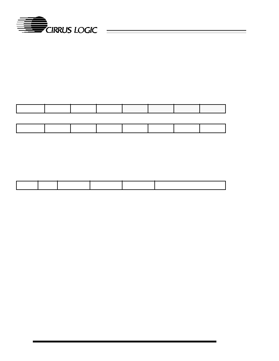
DATA BOOK v1.5
May 1997
52
PROGRAMMING INTERFACE
CL-PS7110
Low-Power System-on-a-Chip
3.2.17 INTMR -- Interrupt Mask Register
The Interrupt Mask register is a 16-bit read/write register used to selectively enable any of the 16 interrupt
sources within the CL-PS7110. The four shaded (see following table) interrupts all generate a fast inter-
rupt request to the ARM710A microprocessor; this causes a jump to processor virtual address
0000.0001C. All other interrupts generate a standard interrupt request; this causes a jump to processor
virtual address 0000.00018. See
Table 1-1 on page 14
for the interrupt allocation. Setting the appropriate
bit in this register enables the corresponding interrupt. All bits are cleared by a
system reset.
3.2.18 LCDCON -- LCD Control Register
The LCD Control register is a 32-bit read/write that controls the size of the LCD screen and the operating
mode of the LCD controller operates in. Refer to
Section 1.2.10
for more information on video buffer map-
ping and the LCD controller.
Video buffer size
The video buffer size field is a 13-bit field that sets the total number of bits
◊
128 (quad
words) in the video display buffer. This is calculated from the formula:
Video buffer size = (Total bits in video buffer / 128)
-
1
For example, for a 640
◊
240 LCD and 4 bits per pixel the size of the video buffer =
640
◊
240
◊
4 = 614400 bits
Video buffer size field = (614400 / 128)
-
1 = 4799 or 0x12BF h.
Line length
The line length field is a 6-bit field that sets the number of pixels in one complete line.
This field is calculated from the formula: Line length = (No. pixels in line / 16)
-
1
For example, for 640
◊
240 LCD Line length = (640 / 16)
-
1 = 39 or 0x27 h.
7
6
5
4
3
2
1
0
EINT3
EINT2
EINT1
CSINT
MCINT
WEINT
BLINT
EXTFIQ
15
14
13
12
11
10
9
8
SSEOTI
UMSINT
URXINT
UTXINT
TINT
RTCMI
TC2OI
TC1OI
31
30
29
25
24
19
18
13
12
0
GSMD
GSEN
AC prescale
Pixel prescale
Line length
Video buffer size

May 1997
53
DATA BOOK v1.5
PROGRAMMING INTERFACE
CL-PS7110
Low-Power System-on-a-Chip
Pixel prescale
The pixel prescale field is a 6-bit field that sets the pixel rate prescale. The pixel rate
is derived from a 36.864-MHz clock and is calculated from the formula:
Pixel rate (MHz) = 36.864 / (pixel prescale + 1)
The pixel rate should be chosen to give a complete screen refresh frequency of
approximately 70 Hz to avoid flicker. Frequencies above 70 Hz should be avoided as
they consume additional power. The pixel prescale value can be expressed in terms
of the LCD size by the formula:
Pixel prescale = (526628 / Total pixels in display)
-
1
The value should be rounded down to the nearest whole number. `0' is illegal and will
result in no pixel clock.
For example: A 640
◊
240 LCD, pixel prescale = 526628 / (640
◊
240)
-
1 = 2.428 (2)
This gives an actual pixel rate of 36.864E6 / 2 + 1 = 12.288 MHz
Which gives an actual refresh frequency of 12.288E6 / (640
◊
240) = 80 Hz.
NOTE:
As the CL2 low pulse time is doubled after every CL1 high pulse (see
Figure 4-7
),
this refresh frequency is only an approximation; the accurate formula is 12.288E6 /
((640
◊
240) + 120) = 79.937 Hz.
AC prescale
The AC prescale field is a 5-bit number that sets LCD AC bias frequency. This fre-
quency is the required AC bias frequency for a given manufacturer's LCD plate. This
frequency is derived from the frequency of the line clock (CL1). The `M' signal toggles
after n+1 counts of the line clock (CL1) where n is the number programmed into the
AC prescale field. This number must be chosen to match the manufacturer's recom-
mendation (normally 13), but must not be exactly divisible by the number of lines in
the display.
GSEN
Grayscale enable bit. Setting this bit enables grayscale output to the LCD. When this
bit is cleared, each bit in the video map directly corresponds to a pixel in the display.
GSMD
Grayscale mode bit. Clearing this bit sets the controller to 2 bits per pixel (4 gray-
scales). Setting sets the controller to 4 bits per pixel (15 grayscales).
3.2.19 TC1D -- Timer Counter 1 Data Register
The Timer Counter 1 Data register is a 16-bit read/write register that sets and reads data to TC1. Any
value written is decremented on the next rising edge of the clock.
3.2.20 TC2D -- Timer Counter 2 Data Register
The Timer Counter 2 Data register is a 16-bit read/write register that sets and reads data to TC2. Any
value written is decremented on the next rising edge of the clock.
3.2.21 RTCDR -- Realtime Clock Data Register
The Realtime Clock Data register is a 32-bit read/write register that sets and reads the binary time in the
RTC. Any value written is incremented on the next rising edge of the 1-Hz clock. All bits in the Realtime
Clock Data register are only cleared by an active NPOR.
3.2.22 RTCMR -- Realtime Clock Match Register
The Realtime Clock Match register is a 32-bit read/write register that sets and reads the binary match time
to RTC. Any value written is compared to the current binary time in the RTC, if they match it asserts the
RTCMI interrupt source.

DATA BOOK v1.5
May 1997
54
PROGRAMMING INTERFACE
CL-PS7110
Low-Power System-on-a-Chip
3.2.23 PMPCON -- Pump Control Register
The DC-to-DC Converter Pump Control register is a 12-bit read/write-only register that sets and controls
the variable mark space ratio drives for two DC-to-DC converters. All bits in this register are cleared by a
system reset.
Drive 0 from battery This 4-bit field controls the on time for the drive 0 DC-to-DC pump while the system
is powered from batteries. Setting these bits to `0' disables this pump, setting these
bits to `1' allows the pump to be driven in a 1:16 duty ratio, 2 in a 2:16 duty ratio, etc.,
up to a 15:16 duty ratio. An 8:16 duty ratio results in a square wave of 96 kHz. The
NEXTPWR input is used to switch between the two on times for `drive0'.
Drive 0 from mains
This 4-bit field controls the on time for the drive 0 DC-to-DC pump while the system
is powered from mains (the DC jack input). Setting these bits to `0' disables this pump;
setting these bits to `1' allows the pump to be driven in a 1:16 duty ratio, 2 in a 2:16
duty ratio, etc., up to a 15:16 duty ratio. An 8:16 duty ratio results in a square wave of
96 kHz. The NEXTPWR input switches between the two on times for drive 0.
Drive 1 pump ratio
This 4-bit field controls the on time for the drive 1 DC-to-DC pump. Setting these bits
to `0' disables this pump, setting these bits to `1' allows the pump to be driven in a 1:16
duty ratio, 2 in a 2:16 duty ratio, etc., up to a 15:16 duty ratio. An 8:16 duty ratio results
in a square wave of 96 kHz.
The state of the output drive pins is latched during power on reset, this latched value is used to determine
the polarity of the drive output. The sense of the DC-to-DC converter control lines is summarized in
Table 3-11
.
3.2.24 CODR -- Codec Interface Data Register
The CODR register is an 8-bit read/write register. Data written to or read from this register is pushed or
popped onto the appropriate 16-byte FIFO buffer. Data from this buffer is then serialized and sent to or
received from the codec sound device. The codec interrupt CSINT is generated repetitively at 1/8th of the
byte transfer rate and the state of the FIFOs can be read in the System Flags register. The net data trans-
fer rate to/from the codec device is 8 Kbytes per second giving an interrupt rate of 1 kHz.
11
8
7
4
3
0
Drive 1 pump ratio
Drive 0 from mains ratio
Drive 0 from battery ratio
Table 3-11. Sense of DC-to-DC Converter Control Lines
Initial State of Drive `n' during
POR
Sense of Drive `n'
Polarity of Bias Voltage
Low
Active high
+VE
High
Active low
-VE

May 1997
55
DATA BOOK v1.5
PROGRAMMING INTERFACE
CL-PS7110
Low-Power System-on-a-Chip
3.2.25 UARTDR -- UART Data Register
The UARTDR register is an 11-bit read and 8-bit write register for all data transfers to or from the internal
UART.
Data written to this register is pushed onto the 16-byte data Tx holding FIFO if the FIFO is enabled; if not,
it is stored in a 1-byte holding register. This write initiates transmission from the UART.
The UART Data Read register comprises the 8-bit data byte received from the UART together with three
bits of error status. Data read from this register is popped from the 16-byte data Rx FIFO if the FIFO is
enabled, if not it is read from a 1-byte buffer register containing the last byte received by the UART. Data
received and error status is automatically pushed onto the Rx FIFO if it is enabled. The Rx FIFO is 10 bits
wide by 16 deep.
FRMERR
UART framing error. This bit is set if the UART detected a framing error while receiv-
ing the associated data byte. Framing errors are caused by non-matching word
lengths or bit rates.
PARERR
UART parity error. This bit is set if the UART detected a parity error while receiving
the data byte.
OVERR
UART overrun error. This bit is set if more data is received by the UART and the FIFO
is full. The Overrun Error bit is not associated with any single character and so is not
stored in the FIFO, if this bit is set, the entire contents of the FIFO is invalid and should
be cleared. This error bit is cleared by reading the UARTDR register.
3.2.26 UBRLCR -- UART Bit Rate and Line Control Register
The UART Bit Rate and Line Control register is a 19-bit read/write register. Writing to this register sets the
bit rate and mode of operation for the internal UART.
Bit rate divisor
This 12-bit field set the bit rate. The bit rate divider is fed by a clock frequency of
3.6864 MHz, it is then further divided internally by 16 to give the bit rate. The formula
to give the divisor value for any bit rate is: Divisor = (230400 / bit rate) - 1. A value of
`0' in this field is illegal.
Table 3-12
shows some example bit rates with the corre-
sponding divisor value.
10
9
8
7
0
OVERR
PARERR
FRMERR
Rx data
31
19
18
17
16
15
14
13
12
11
0
WRDLEN
FIFOEN
XSTOP
EVENPRT
PRTEN
BREAK
Bit rate divisor

DATA BOOK v1.5
May 1997
56
PROGRAMMING INTERFACE
CL-PS7110
Low-Power System-on-a-Chip
BREAK
Setting this bit drives the Tx output active (high) to generate a break.
PRTEN
Parity enable bit. Setting this bit enables parity detection and generation.
EVENPRT
Even parity bit. Setting this bit sets parity generation and checking to even parity,
clearing it sets odd parity. This bit has no effect if the PRTEN bit is clear.
XSTOP
Extra stop bit. Setting this bit causes the UART to transmit two stop bits after each
data byte, clearing it transmits one stop bit after each data byte.
FIFOEN
Set to enable FIFO buffering of Rx and Tx data. Clear to disable the FIFO, that is, set
its depth to one byte.
WRDLEN
This 2-bit field selects the word length according to
Table 3-13
.
3.2.27 PALLSW Least-Significant Word-LCD Palette Register
The least- and most-significant Word-LCD Palette registers make up a 64-bit read/write register, which
maps the logical pixel value to a physical grayscale level. The 64-bit register is made up of 16
◊
4-bit nib-
bles, each nibble defines the grayscale level associated with the appropriate pixel value. If the LCD con-
troller is operating in two bits per pixel, only the lower four nibbles are valid D[15:0] in the least-significant
Table 3-12. Internal UART Bit Rates
Divisor Value
Bit Rate
1
115200
2
76800
3
57600
5
38400
11
19200
15
14400
23
9600
95
2400
191
1200
2094
110
Table 3-13. UART Word Length
WRDLEN
Word Length
00
5 bits
01
6 bits
10
7 bits
11
8 bits

May 1997
57
DATA BOOK v1.5
PROGRAMMING INTERFACE
CL-PS7110
Low-Power System-on-a-Chip
word), similarly one bit per pixel means only the lower two nibbles are valid D[7:0] in the least-significant
word). The pixel-to-grayscale level assignments are shown in
Table 3-14
and
Table 3-15
.
PALMSW Most-Significant Word-LCD Palette Register
See PALLSW description in
Section 3.2.27
.
The actual physical color and pixel duty ratio for the grayscale values is shown in
Table 3-16
. Note that
colors 8≠15 are the inverse of colors 7≠0 respectively; this means that colors 7 and 8 are identical. The
steps in the grayscale are nonlinear but have been chosen to give a close approximation to perceived lin-
ear grayscales. The is due to the eye being more sensitive to changes in gray level close to 50% gray.
Table 3-14. Least-Significant Word Palette Assignments
31:28
27:24
23:20
19:16
15:12
11:8
7:4
3:0
Grayscale
value for
pixel value 7
Grayscale
value for
pixel value 6
Grayscale
value for
pixel value 5
Grayscale
value for
pixel value 4
Grayscale
value for
pixel value 3
Grayscale
value for
pixel value 2
Grayscale
value for
pixel value 1
Grayscale
value for
pixel value 0
Table 3-15. Most-Significant Word Palette Assignments
31:28
27:24
23:20
19:16
15:12
11:8
7:4
3:0
Grayscale
value for
pixel value
15
Grayscale
value for
pixel value
14
Grayscale
value for
pixel value
13
Grayscale
value for
pixel value
12
Grayscale
value for
pixel value
11
Grayscale
value for
pixel value
10
Grayscale
value for
pixel value 9
Grayscale
value for
pixel value 8
Table 3-16. Grayscale Value to Color Mapping
Grayscale
Value
Duty Cycle
% Pixels
Lit
% Step
change
0
0
0%
11.1%
1
1/9
11.1%
8.9%
2
1/5
20.0%
6.7%
3
4/15
26.7%
6.6%
4
3/9
33.3%
6.7%
5
2/5
40.0%
5.4%
6
4/9
44.4%
5.6%
7
1/2
50.0%
0.0%
8
1/2
50.0%
5.6%
9
5/9
55.6%
5.4%
10
3/5
60.0%
6.7%
11
6/9
66.7%
6.6%

DATA BOOK v1.5
May 1997
58
PROGRAMMING INTERFACE
CL-PS7110
Low-Power System-on-a-Chip
3.2.28 SYNCIO Synchronous Serial Interface Data Register
SYNCIO is a 16-bit read/write register. The data written to the SYNCIO register configures the SSI, and
the least-significant byte is serialized and transmitted out of the synchronous serial interface to configure
an external ADC, bit D7 (the MSB) first. The transfer clock automatically starts at the programmed fre-
quency, and a synchronization pulse is issued. The ADCIN pin is sampled on every clock edge, and the
result is shifted in to the SYNCIO read register.
During data transfer the SSIBUSY bit is set high, at the end of a transfer the SSEOTI interrupt is asserted.
This interrupt is cleared by reading the SYNCIO register. The data read from the SYNCIO register is the
last sixteen bits shifted out of the ADC. The length of the data frame can be programmed by writing to the
SYNCIO register, this allows many different ADCs to be accommodated.
Table 3-17
defines the bits in the
SYNCIO register.
3.2.29 STFCLR -- Clear All Start Up Reason Flags Location
A write to this location clears all the start-up reason flags in the System Flags Status register (SYSFLG).
3.2.30 BLEOI -- Battery Low End of Interrupt
A write to this location clears the interrupt generated by a low battery (falling BATOK with NEXTPWR
high).
12
11/15
73.3%
6.7%
13
4/5
80.0%
8.9%
14
8/9
88.9%
11.1%
15
1
100%
≠
Table 3-17. Bits in SYNCIO Write Register
15
24
14
16
13
16
12
8
7
0
Reserved
TXFRMEN
SMCKEN
Frame length
ADC Configuration byte
ADC configuration
8-bit configuration data to be sent to the ADC.
Frame length
The 5-bit Frame length field is the total number of shift clocks required to complete a data transfer.
For many ADCs this is 25, 8 for configuration byte + 1 null bit + 16 bits.
SMCKEN
Setting this bit enables a free-running sample clock at the programmed ADC clock frequency to be
output on the SMPLCK pin.
TXFRMEN
Setting this bit causes an ADC data transfer to be initiated; the value in the ADC configuration field
is shifted out to the ADC, and depending on the frame length programmed, a number of bits is cap-
tured from the ADC. If the SYNCIO register is written to with the TXFRMEN bit low, no ADC trans-
fer occurs, but the Frame length and SMCKEN bits are affected.
Table 3-16. Grayscale Value to Color Mapping
(cont.)

May 1997
59
DATA BOOK v1.5
PROGRAMMING INTERFACE
CL-PS7110
Low-Power System-on-a-Chip
3.2.31 MCEOI -- Media Changed End of Interrupt
A write to this location clears the interrupt generated by a rising edge of the MEDCHG input pin.
3.2.32 TEOI -- Tick End of Interrupt Location
A write to this location clears the current pending tick interrupt and watchdog interrupt.
3.2.33 TC1EOI TC1 -- End of Interrupt Location
A write to this location clears the under-flow interrupt generated by TC1.
3.2.34 TC2EOI TC2 -- End Of Interrupt Location
A write to this location clears the under-flow interrupt generated by TC2.
3.2.35 RTCEOI -- RTC Match End Of Interrupt
A write to this location clears the RTC match interrupt.
3.2.36 UMSEOI -- UART Modem Status Changed End of Interrupt
A write to this location clears the modem status changed interrupt.
3.2.37 COEOI -- Codec End of Interrupt Location
A write to this location clears the sound interrupt (CSINT).
3.2.38 HALT -- Enter Idle State Location
A write to this location places the system into the
idle state by halting the clock to the processor until an
interrupt is generated. A write to this location while there is an active interrupt has no effect. If the
idle
state is entered with no interrupts enabled, there is no mechanism for exiting the state except for a system
reset.
3.2.39 STDBY -- Enter Standby State Location
A write to this location places the system into the
standby state by halting the main oscillator. It automat-
ically switches the DRAMs to self-refresh if the RFSHEN bit is set in the DRAM Refresh Period register.
All transitions to the
standby state are synchronized with DRAM cycles. A write to this location while there
is an active interrupt has no effect.

DATA BOOK v1.5
May 1997
60
ELECTRICAL SPECIFICATIONS
CL-PS7110
Low-Power System-on-a-Chip
4.
ELECTRICAL SPECIFICATIONS
4.1
Absolute Maximum Ratings
DC supply voltage
-
0.5 volts to
+
6 volts
DC input/output voltage
-
0.5 volts to V
DD
+
0.5 volts
DC input current
±
20 mA
Storage temperature
-
40
∞
C to
+
125
∞
C
Lead temperature
+
300
∞
C
4.2
Recommended Operating Conditions
DC supply voltage
+
3.0 volts to
+
3.6 volts
DC input/output voltage
0 to V
DD
DC input current
±
15 mA
Operating temperature
0
∞
C to
+
70
∞
C

May 1997
61
DATA BOOK v1.5
ELECTRICAL SPECIFICATIONS
CL-PS7110
Low-Power System-on-a-Chip
4.3
DC Characteristics
All characteristics are specified at
V
DD
= 3.0 to 3.6 volts and V
SS
= 0 volts over an operating temperature
of 0
∞
C to +70
∞
C.
a
Assumes buffer has no pull-up or pull-down resistors.
Table 4-1.
DC Characteristics
Symbol
Parameter
MIN
MAX
Units
Conditions
VIH
CMOS input high voltage
0.7
◊
V
DD
V
DD
+
0.3
V
VIL
CMOS input low voltage
-
0.3
0.2
◊
V
DD
V
VT+
Schmitt trigger positive going
threshold
1.52
2.26
V
VT-
Schmitt trigger negative going
threshold
0.72
1.29
V
VHST
Schmitt trigger hysteresis
0.64
1.13
V
VIL to VIH
VOH
CMOS output high voltage
Output drive 1 and 2
Output drive 3 and 4
V
DD
-
0.3
V
DD
-
1.0
V
DD
-
1.0
V
V
V
IOH = 0.8 mA
IOH = 3 mA
IOH = 12 mA
VOL
CMOS output low voltage
Output drive 1 and 2
Output drive 3 and 4
0.1
0.5
0.5
V
V
V
IOL = -0.8 mA
IOL = -3 mA
IOL = -12 mA
IIN
Input leakage current
-
10
+
10
µ
A
VIN = V
DD
or GND
IOZ
Output tristate leakage current
a
-
10
+
10
µ
A
VOUT = V
DD
or GND
CIN
Input capacitance
5
pF
COUT
Output capacitance
5
pF
CI/O
Transceiver capacitance
5
pF
IDD
startup
Startup current consumption
50
µ
A
Initial 100 ms from power up,
32-kHz oscillator not stable,
POR signal at VIL, all other I/O
static, VIH = V
DD
±
0.1 V, VIL =
GND
±
0.1 V
IDD
standby
Standby current consumption
20
µ
A
Just 32-kHz oscillator running,
all other I/O static, VIH = V
DD
±
0.1 V, VIL = GND
±
0.1 V
IDD
idle
Idle current consumption
5
mA
Both oscillators running, CPU
static, LCD refresh active, VIH
= V
DD
±
0.1 V, VIL = GND
±
0.1
V
IDD
operating
Operating current consumption
50
mA
All system active, running typi-
cal program
VDD
standby
Standby supply voltage
2.2
V
Minimum standby voltage for
state retention and RTC opera-
tion only
DATA BOOK v1.5
May 1997
62
ELECTRICAL SPECIFICATIONS
CL-PS7110
Low-Power System-on-a-Chip
4.4
AC Characteristics
All characteristics are specified at
V
DD
= 3.0 to 3.6 volts and V
SS
= 0 volts over an operating temperature
of 0
∞
C to +70
∞
C. Parameters marked with an asterisk (*) are not fully tested.
Table 4-2.
AC Characteristics
Symbol
Parameter
MIN
MAX
Units
t
1
Falling CS to data bus High-Z
0*
25*
ns
t
2
Address change to valid write data
0
35
ns
t
3
DATA in to falling EXPCLK setup time
18
≠
ns
t
4
DATA in to falling EXPCLK hold time
0
≠
ns
t
5
EXPRDY to falling EXPCLK setup time
18
≠
ns
t
6
Falling EXPCLK to EXPRDY hold time
0
50
ns
t
7
Rising NMWE to data invalid hold time
5
≠
ns
t
8
Sequential data valid to falling NMWE setup time
-
10
10
ns
t
9
Row address to falling NRAS setup time
5
≠
ns
t
10
Falling NRAS to row address hold time
25
≠
ns
t
11
Column address to falling NCAS setup time
2
≠
ns
t
12
Falling NCAS to column address hold time
25
≠
ns
t
13
Write data valid to falling NCAS setup time
2
≠
ns
t
14
Write data valid from falling NCAS hold time
50
≠
ns
t
15
LCD CL2 low time
80
3,475
ns
t
16
LCD CL2 high time
80
3,475
ns
t
17
LCD Rising CL2 to rising CL1 delay
0
25
ns
t
18
LCD Falling CL1 to rising CL2
80
3,475
ns
t
19
LCD CL1 high time
80
3,475
ns
t
20
LCD Falling CL1 to falling CL2
200
6,950
ns
t
21
LCD Falling CL1 to FRM toggle
300
10,425
ns
t
22
LCD Falling CL1 to M toggle
-
10
20
ns
t
23
LCD Rising CL2 to display data change
-
10
20
ns
t
24
Falling EXPCLK to address valid
≠
30
ns
t
25
Initial data valid to falling NMWE setup time
5
≠
ns
t
EXTRD
Zero-wait-state memory read access time
70
≠
ns
t
EXWR
Zero-wait-state memory write access time
70
≠
ns
t
RC
DRAM cycle time
150
≠
ns

May 1997
63
DATA BOOK v1.5
ELECTRICAL SPECIFICATIONS
CL-PS7110
Low-Power System-on-a-Chip
Figure 4-1. Expansion and ROM Read Timing
NOTES:
1) t
EXRD
= 80 ns for minimum wait states and a main oscillator frequency of 18.432 MHz. This time can be
t
RAC
Access time from RAS
70
≠
ns
t
RP
RAS precharge time
70
≠
ns
t
CAS
CAS pulse width
20
≠
ns
t
CP
CAS precharge in Page mode
12
≠
ns
t
PC
Page mode cycle time
45
≠
ns
t
CSR
CAS set-up time for auto refresh
15
≠
ns
t
RAS
RAS pulse width
80 *
≠
ns
Table 4-2.
AC Characteristics
(cont.)
EXPCLK
BUS HELD
t
5
t
1
t
6
t
4
t
3
t
24
NMOE
A[27:0]
D[31:0]
DATA IN
DATA IN
WORD
NCS[3:0]
CS[7:4]
EXPRDY
t
EXRD
t
EXRD
t
3
t
4
Consecutive expansion read cycles with minimum wait states

DATA BOOK v1.5
May 1997
64
ELECTRICAL SPECIFICATIONS
CL-PS7110
Low-Power System-on-a-Chip
extended by integer multiples of the clock period (54 ns), by either driving EXPRDY low and or by program-
ming a number of wait states. EXPRDY is sampled on the falling edge of EXPCLK before the data transfer,
if low at this point the transfer is delayed by one clock period where EXPRDY is sampled again. EXPCLK
need not be referenced when driving EXPRDY but is shown for clarity.
2) Consecutive reads with sequential access enabled are identical except that the sequential access wait state
field is used to determine the number of wait states.
Figure 4-2. Expansion and ROM Write Timing
NOTES:
1) t
EXWR
= 80 ns maximum for zero wait states. This time can be extended by integer multiples of the clock
period (54 ns), by either driving EXPRDY low and or by programming a number of wait states. EXPRDY is
sampled on the falling edge of EXPCLK before the data transfer, if low at this point the transfer is delayed by
one clock period where EXPRDY is sampled again. EXPCLK need not be referenced when driving EXPRDY
but is shown for clarity.
2) Consecutive writes with sequential access enabled are identical except that the sequential access wait state
field is used to determine the number of wait states.
3) Zero wait states for sequential writes is not supported, one state automatically is added.
EXPCLK
BUS HELD
t
5
t
8
t
6
t
2
NMWE
A[27:0]
D[31:0]
WRITE DATA
WORD
NCS[3:0]
CS[7:4]
EXPRDY
t
7
Consecutive expansion write cycles with minimum wait states
t
2
t
EXWR
t
EXWR
t
8
t
24
WRITE DATA

May 1997
65
DATA BOOK v1.5
ELECTRICAL SPECIFICATIONS
CL-PS7110
Low-Power System-on-a-Chip
Figure 4-3. DRAM Read Cycles
NOTES:
1) t
RC
(read cycle time) = 160 ns maximum
2) t
RAC
(access time from RAS) = 80 ns maximum
3) t
RP
(RAS precharge time) = 80 ns maximum
4) t
CAS
(CAS pulse width) = 25 ns maximum
5) t
CP
(CAS precharge in Page mode = 25 ns maximum
6) t
PC
(Page mode cycle time) = 50 ns minimum at maximum
7) Word reads shown, for byte reads only one of CAS[3:0] is active, CAS0 for byte 0, etc.
t
10
t
9
DRA[12:0]
t
RC
MCLK
ROW
COL
ROW
COL 1
COL 2
COL n
RAS[3:0]
CAS[3:0]
D[31:0]
NMOE
NMWE
WORD
WRITE
t
RAS
t
RP
t
PC
t
CP
t
CAS
t
11
t
12
1
2
n
DRAM word read followed by Page mode read (MCLK shown for reference only)
DATA BOOK v1.5
May 1997
66
ELECTRICAL SPECIFICATIONS
CL-PS7110
Low-Power System-on-a-Chip
Figure 4-4. DRAM Write Cycles
NOTES:
1) t
RC
(Write cycle time) = 160 ns minimum at MCLK = 18.432 MHz
2) t
RAC
(Write access time from RAS) = 80 ns minimum at MCLK = 18.432 MHz
3) t
RP
(RAS precharge time) = 80 ns minimum at MCLK = 18.432 MHz
DATA OUT 2
DATA OUT 1
t
13
CAS[3:0]
D[31:0]
NMOE
WORD
DRA[12:0]
RAS[3:0]
WORD write followed by sequential word write to DRAM (MCLK shown for reference only)
t
14
t
RAS
t
11
MCLK
ROW
COL
ROW
COL 1
COL 2
COL n
t
9
t
10
t
RC
t
RP
t
12
t
CAS
t
CP
t
PC
WRITE
NMWE
DATA OUT
DATA OUT n

May 1997
67
DATA BOOK v1.5
ELECTRICAL SPECIFICATIONS
CL-PS7110
Low-Power System-on-a-Chip
4) t
CAS
(CAS pulse width) = 25 ns minimum at MCLK = 18.432 MHz
5) t
CP
(CAS precharge in Page mode = 80 ns minimum at MCLK = 18.432 MHz
6) t
PC
(Page mode cycle time) = 100 ns minimum at MCLK = 18.432 MHz
7) Word writes shown, for byte writes only one of CAS[3:0] is active, CAS0 for byte 0, etc.
Figure 4-5. Video Quad Word Read
NOTES:
1) Timings are the same as Page mode word reads.
2) t
VACC
(video access cycle time) = 326 ns at MCLK = 18.432 MHz
CAS[3:0]
D[31:0]
NMOE
RAS0
Video quad-word read (MCLK shown for reference only)
MCLK
ROW
COL 0
COL 1
t
RP
t
CAS
t
CP
t
PC
NMWE
DRA[12:0]
COL 2
COL 3
0
t
VACC
1
2
3

DATA BOOK v1.5
May 1997
68
ELECTRICAL SPECIFICATIONS
CL-PS7110
Low-Power System-on-a-Chip
Figure 4-6. DRAM CAS-Before-RAS Refresh Cycle
NOTES:
1) t
CSA
(CAS set-up time) = 25 ns minimum at MCLK = 18.432 MHz
2) t
RAS
(RAS pulse width) = 80 ns minimum at MCLK = 18.432 MHz
3) t
RC
(cycle time) = 160 ns minimum at MCLK = 18.432 MHz
4) When DRAMs are placed in self-refresh (entering standby) the same timings apply, but t
RAS
is extended
indefinitely.
HELD
CAS[3:0]
D[31:0]
NMOE
DRA[12:0]
RAS[3:0]
DRAM CAS-before-RAS refresh cycle (MCLK shown for reference only)
t
RAS
MCLK
ROW
COL
t
CSA
NMWE
HELD
t
RC
May 1997
69
DATA BOOK v1.5
ELECTRICAL SPECIFICATIONS
CL-PS7110
Low-Power System-on-a-Chip
Figure 4-7. LCD Controller Timing
NOTES:
1) This diagram shows the end of a line.
2) If FRM is high during the CL1 pulse, this marks the first line in the display.
3) CL2 low time is doubled during the CL1 high pulse.
M
CL1
FRM
t
18
CL2
t
23
DD[3:0]
t
22
t
17
t
15
t
16
t
21
t
19
t
20

DATA BOOK v1.5
May 1997
70
ELECTRICAL SPECIFICATIONS
CL-PS7110
Low-Power System-on-a-Chip
4.5
I/O Buffer Characteristics
All I/O buffers on the CL-PS7110 are CMOS threshold input bidirectional buffers except the oscillator and
power pads. Notional input signals only enable the output buffer during Pin Test mode. All output buffers
are disabled during System Test (High-Z) mode. All buffers have a standard CMOS threshold input stage
apart from the Schmitt inputs and CMOS, slew-rate-controlled output stages to reduce system noise.
Table 4-3
defines the I/O buffer output characteristics.
NOTE:
1) All propagation delays are specified at 50%
V
DD
to 50%
V
DD
; all rise times are specified as 10%
V
DD
to 90%
V
DD
,
and all fall times are specified as 90%
V
DD
to 10%
V
DD
.
2) Pull-up current = 50
µ
A typical at
V
DD
= 3.3 volts.
4.6
Test Modes
The CL-PS7110 supports a number of hardware-activated test modes; these are activated by the pin
combinations shown in
Table 4-4
. All latched signals will only alter test modes while NPOR is low, and
their state is latched on the rising edge of NPOR. This allows these signals be used normally during var-
ious test modes; for example, the NURESET input can be used normally when the device is set into Func-
tional Test (EPB) mode.
Table 4-3.
I/O Buffer Output Characteristics
Buffer Type
Drive Current
Propagation Delay
(MAX)
Rise Time
(MAX)
Fall Time
(MAX)
Load
I/O strength 1
±
3 mA
15 ns
18 ns
15 ns
50 pF
I/O strength 2
±
3 mA
15 ns
15 ns
15 ns
50 pF
I/O strength 3
±
12 mA
12 ns
15 ns
13 ns
50 pF
I/O strength 4
±
12 mA
12 ns
180 ns
80 ns
1000 pF
Table 4-4.
CL-PS7110 Hardware Test Modes
Test Mode
Latched
MEDCHG
Latched
PE0
Latched
NURESET
NTEST0
NTEST1
Normal operation (32-bit boot)
0
0
X
1
1
Normal operation (8-bit boot)
0
1
X
1
1
Alternative test ROM boot
1
X
X
1
1
Oscillator/PLL bypass
X
X
X
1
0
Functional Test (EPB)
X
X
1
0
1
Oscillator/PLL Test
X
X
0
0
1
Pin Test
X
X
1
0
0
System Test (all High-Z)
X
X
0
0
0
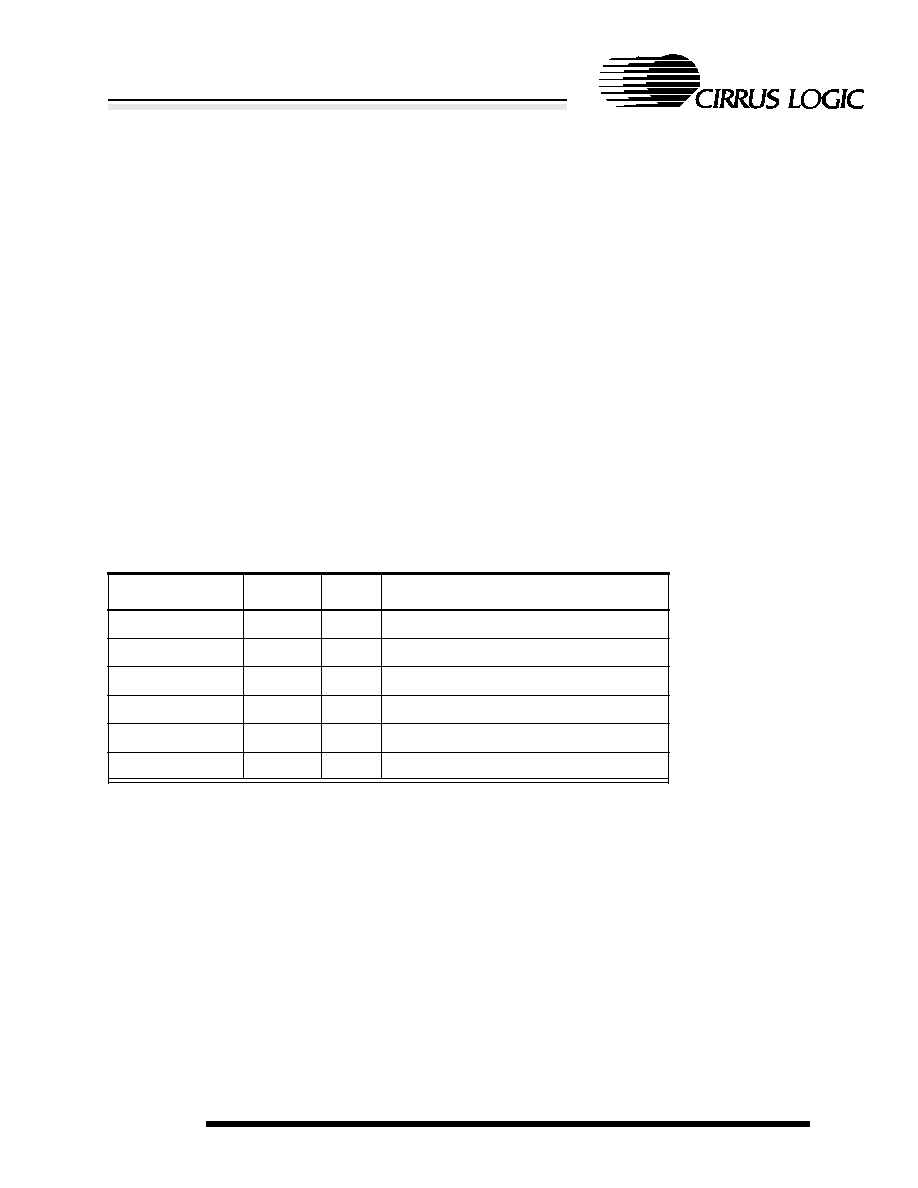
May 1997
71
DATA BOOK v1.5
ELECTRICAL SPECIFICATIONS
CL-PS7110
Low-Power System-on-a-Chip
Within each test mode a selection of pins are used as multiplexed outputs or inputs to provide/monitor the
test signals unique to that mode.
4.6.1
Oscillator and PLL Bypass Mode
This mode is selected by NTEST0 = 1, NTEST1 = 0.
In this mode all the internal oscillators and PLL are disabled and the appropriate crystal oscillator pins
become the direct external oscillator inputs bypassing the oscillator and PLL. MOSCIN must be driven by
a 36.864-MHz clock source and RTCOUT by a 32.768-kHz source. In addition the OSCEN (oscillator
enable) signal is multiplexed out on Port C bit 0 to control the external oscillator. It is driven logic to level
low to disable the oscillator. The functionality of the CL-PS7110 is not affected in any other way during
this test mode.
4.6.2
Functional (EPB) Test Mode
This mode is selected by NTEST0 = 0, NTEST1 = 1, Latched NURESET = 1
Functional EPB (embedded peripheral bus) Test mode is used for the running test patterns, both through
the EPB external test interface and for any other patterns. It is for testing individual peripherals and the
ARM710A microprocessor. The PLL is automatically bypassed in this mode. In this mode various pins are
used as control inputs or outputs; these are listed in
Table 4-5
.
4.6.3
Oscillator and PLL Test Mode
This mode is selected by NTEST0 = 0, NTEST1 = 1, Latched NURESET = 0
This test mode enables the main oscillator and output various buffered clock and test signals derived from
the main oscillator, PLL, and 32-kHz oscillator. All internal logic in the CL-PS7110 is static and isolated
from the oscillators with the exception of the 6-bit ripple counter used to generate 576-kHz and the real-
time clock divide chain. Port A is used to drive the inputs of the PLL directly and the various clock and PLL
outputs are monitored on the COL pins.
Table 4-6
defines the CL-PS7110 signal pins used in this test
mode.
Table 4-5.
EPB Test Mode Signal Assignment
Signal
I/O
Pin
Function
TSTA
I
PA0
EPB test control A
TSTB
I
PA1
EPB test control B
TSTSTART
I
PA2
Fast start speed up RTC divider chain
TSTDIRCLK
I
PA3
Insertion point for EPB test clock
TSTVCOUNT
I
PA4
Video Address counter increments faster
TACK
O
word
EPB test acknowledge output

DATA BOOK v1.5
May 1997
72
ELECTRICAL SPECIFICATIONS
CL-PS7110
Low-Power System-on-a-Chip
4.6.4
Pin Test Mode
This mode is selected by NTEST0 = 0, NTEST1 = 0, Latched NURESET = 1.
This test mode allows a simple ICT tester to check if all pins on the CL-PS7110 are correctly soldered to
the PCB. This mode does this by back-driving each pin in turn, and checking the response on one desig-
nated pin (the COL7 pin).
A parity bit is generated and output on the COL7 pin; this parity bit is the XOR of the input from every
CL-PS7110 signal pin except for the two test inputs. The input pad of each signal is fed into this XOR gate
regardless of signal type. Externally driving (back-driving) any signal pin from its reset state causes a tran-
sition of the COL7 pin.
Table 4-6
defines the rest state for all CL-PS7110 output pins. As Pin Test mode
is entered, the states of all CL-PS7110 inputs are latched, and forced back out on the pins. Thus ALL pins
(except the two test pins) are configured as outputs in this mode. This ensures only a `good' solder joint
passes the pin test. When not in Pin Test mode, the XOR chain is disabled and cannot toggle to save
power.
It is essential in Pin Test mode that the NURESET pin is kept in the default (HIGH) state except when it
is being tested itself. This ensures that NPOR can be safely included in the pin test chain without affecting
the test mode.
a
These inputs are INVERTED before being passed to the PLL to ensure that the default state of the port
(all `0') maps onto the correct default state of the PLL (TSEL = 1, XTALON = 1, PLLON = 1, D0 = 0, D1
= 1, PLLBP = 0). This state produces the correct frequencies as shown in
Table 4-6
. Any other combina-
tions are for testing the oscillator and PLL and should not be used in the circuit.
Table 4-6.
Oscillator and PLL Test Mode Signals
Signal
I/O
Pin
Function
TSEL
a
I
PA5
PLL test select
XTALON
a
I
PA4
Enable to oscillator circuit
PLLON
a
I
PA3
Enable to PLL circuit
DN0
I
PA2
Selects other frequencies from PLL with DN0
DN1
a
I
PA1
Selects other frequencies from PLL with DN1
PLLBP
I
PA0
Bypasses PLL
RTCCLK
O
COL0
Output of RTC oscillator
CLK1
O
COL1
1-Hz clock from RTC divide chain
OSC36
O
COL2
36-MHz PLL main output
CLK576K
O
COL4
576 kHz divided-down as above
VTEST
O
COL5
Analog output of VCO loop filter
VREF
O
COL6
VCO output for test

May 1997
73
DATA BOOK v1.5
ELECTRICAL SPECIFICATIONS
CL-PS7110
Low-Power System-on-a-Chip
4.6.5
High-Z (System) Test Mode
This mode selected by NTEST0 = 0, NTEST1 = 0, Latched NURESET = 0.
This test mode asynchronously disables all output buffers on the CL-PS7110; this has the effect of remov-
ing the CL-PS7110 from the PCB so that other devices on the PCB can be tested. The internal state of
the CL-PS7110 is not altered directly by this test mode.
4.6.6
Test ROM Mode
This mode is entered by holding the MEDCHG input high during the transition from low to high of the
NPOR input pin. If Test ROM mode is enabled the processor boots from an alternative 8-bit test ROM.
The effect of this test mode is to reverse the decoding for all expansion selects.
Table 4-7
shows this
decoding. In addition the sense of bit 1 in the Memory Configuration register is reversed so that 00 = 8-
bit access,
Table 4-7
lists the chip select address ranges, and
Table 4-8
, the bus width field combinations
during Test ROM mode. This has the effect of making the boot ROM an 8-bit device connected to CS7.
Table 4-7.
Chip Select Address Ranges During Test ROM Mode
Address Range
Expansion Chip Select in Test ROM Mode
0000.0000≠0FFF.FFFF
CS7
1000.0000≠1FFF.FFFF
CS6
2000.0000≠2FFF.FFFF
CS5
3000.0000≠3FFF.FFFF
CS4
4000.0000≠4FFF.FFFF
NCS3
5000.0000≠5FFF.FFFF
NCS2
6000.0000≠6FFF.FFFF
NCS1
7000.0000≠7FFF.FFFF
NCS0
Table 4-8.
Expansion and ROM Interface Bus Width During Test ROM Mode
Bus Width Field in ROM Test Mode
Expansion Transfer Mode
00
8-bit-wide bus access
01
PCMCIA mode
10
32-bit-wide bus access
11
16-bit-wide bus access

DATA BOOK v1.5
May 1997
74
ELECTRICAL SPECIFICATIONS
CL-PS7110
Low-Power System-on-a-Chip
4.6.7
Software-Selectable Test Functionality
When bit 11 of the SYSCON register is set HIGH, all internal EPB accesses are output on the main
address and data buses as though they were external accesses to the address space addressed by CS6.
Hence CS6 handles a dual role: It is active as the strobe for internal accesses and for any accesses to
the standard address range for CS6. Additionally in this mode, the following internal signals are multi-
plexed out of the device on port pins:
NOTE: Port E defaults to input so PE1 and PE2 has to be programmed to output mode to observe NIRQ and NFIQ
on these signals.
Signal
I/O
Pin
Function
NIRQ
O
PE1
NIRQ interrupt to CPU
NFIQ
O
PE2
NFIQ interrupt to CPU

May 1997
75
DATA BOOK v1.5
PACKAGE SPECIFICATIONS
CL-PS7110
Low-Power System-on-a-Chip
5.
PACKAGE SPECIFICATIONS
5.1
208-Pin VQFP Package Outline Drawing
NOTES:
1) Dimensions are in millimeters (inches), and controlling dimension is millimeter.
2) Drawing above does not reflect exact package pin count.
3) Before beginning any new design with this device, please contact Cirrus Logic for the latest package information.
Pin 1 Indicator
29.60 (1.165)
30.40 (1.197)
0.17 (0.007)
0.27 (0.011)
27.80 (1.094)
28.20 (1.110)
0.50
(0.0197)
BSC
29.60 (1.165)
30.40 (1.197)
27.80 (1.094)
28.20 (1.110)
1.35 (0.053)
1.45 (0.057)
0
∞
MIN
7
∞
MAX
0.09 (0.004)
0.20 (0.008)
1.40 (0.055)
0.45 (0.018)
0.75 (0.030)
0.05 (0.002)
1.00 (0.039) BSC
Pin 1
Pin 208
1.60 (0.063)
0.15 (0.006)
CL-PS7110
208-Pin VQFP

DATA BOOK v1.5
May 1997
76
ORDERING INFORMATION
CL-PS7110
Low-Power System-on-a-Chip
6.
ORDERING INFORMATION
The order number for the device is:
CL ≠ PS7110 ≠ VC ≠ A
Cirrus Logic, Inc.
Product Line:
Part Number
Package Type:
Temperature Range:
Revision
C = Commercial -- 0≠70
∞
C
V = Very-Low-Profile Quad Flat Pack
Contact Cirrus Logic for up-to-date information on revisions.
Portable Products
I = Industrial -- -25≠70
∞
C

May 1997
77
DATA BOOK v1.5
BIT INDEX
CL-PS7110
Low-Power System-on-a-Chip
Numerics
64-Hz tick interrupt (TINT)
51
A
AC prescale
53
B
Battery low interrupt (BLINT)
50
Bit rate divisor
55
Bit to drive buzzer (BZTOG)
44
BOOT8BIT
47
BREAK
56
Buzzer Drive (BZMOD)
44
C
Clear to send (CTS)
46
Codec interface enable Rx (CDENRX)
44
Codec interface enable Tx (CDENTX)
44
Codec Rx FIFO empty (CRXFE)
47
Codec sound interrupt (CSINT)
50
Codec Tx FIFO full (CTXFF)
47
Cold start flag (CLDFLG)
46
D
Data carrier detect (DCD)
46
Data set ready (DSR)
46
Debug enable (DBGEN)
44
Display ID nibble (DID)
46
DRAM refresh enable (RFSHEN)
49
DRAM refresh rate (RFDIV)
50
Drive 0 from battery
54
Drive 0 from mains
54
Drive 1 pump ratio
54
E
Even parity (EVENPRT)
56
Expansion clock enable (CLKEN)
49
External expansion clock enable (EXCKEN)
44
External fast interrupt (EXTFIQ)
50
External interrupt input 1 (EINT1)
50
External interrupt input 2 (EINT2)
51
External interrupt input 3 (EINT3)
51
Extra stop (XSTOP)
56
F
FIFO buffering of Rx and Tx data enable (FIFOEN)
56
G
Grayscale enable (GSEN)
53
Grayscale mode (GSMD)
53
H
HP SIR protocol encoding enable (SIREN)
44
I
Internal UART enable (UARTEN)
44
Internal UART modem status changed interrupt
(UMSINT)
51
Internal UART receive FIFO half-full interrupt (URXINT)
51
Internal UART transmit FIFO half-empty interrupt
(UTXINT)
51
Inverted NDCDET enable (DCDET)
46
IrDA Tx mode (IRTXM)
45
K
Keyboard Scan
43
L
LCD enable bit (LCDEN)
44
Line length
52
M
Media changed direct read (MCDR)
46
Media changed interrupt (MCINT)
50
Microwire/SPI peripheral clock speed select
(ADCKSEL)
45
N
New battery flag (NBFLG)
46
P
Parity enable (PRTEN)
56
Pixel prescale
53
Power fail flag (PFFLG)
46
R
Reset flag (RSTFLG)
46
RTC compare match interrupt (RTCMI)
51
RTC divisor output (RTCDIV)
46
S
Sequential access enable (SQAEN)
49
BIT INDEX

DATA BOOK v1.5
May 1997
78
BIT INDEX
CL-PS7110
Low-Power System-on-a-Chip
Synchronous serial interface end-of-transfer interrupt
(SSEOTI)
51
T
TC1 under-flow interrupt (TC1OI)
51
TC2 under-flow interrupt (TC2OI)
51
Timer Counter 1 (TC1)
44
Timer Counter 1 clock source (TC1S)
44
Timer Counter 2 (TC2M)
44
Timer Counter 2 clock source (TC2S)
44
U
UART framing error (FRMERR)
55
UART overrun error (OVERR)
55
UART parity error (PARERR)
55
UART receiver FIFO empty (URXFE)
46
UART transmit FIFO full (UTXFF)
46
UART transmitter busy (UBUSY)
46
V
Version ID (VERID)
47
Video buffer size
52
W
Wake-up direct read (WUDR)
46
Wake-up disable (WAKEDIS)
45
Wake-up on (WUON)
46
Watch dog expired interrupt (WEINT)
50
Word length enable (WRDLEN)
56

May 1997
79
DATA BOOK v1.5
INDEX
CL-PS7110
Low-Power System-on-a-Chip
Numerics
208-pin VQFP package
75
208-pin VQFP pin diagram
31
A
abbreviations
9
acronyms
9
ARM710A
data sheet
12
microprocessor
11≠
13
, 18≠19, 28≠29, 39, 44, 52, 71
World-Wide-Web site
12
B
buffer
I/O characteristics
70
bus conversion
48
bus width conversion
48
C
chip select address ranges
ROM mode
73
conventions
abbreviations
9
acronyms
9
numbers and units
10
D
DRAM controller
19
address mapping
20
refresh register
21,
49
E
EPB Test mode signal assignment
71
F
functional description
block diagram
11
overview
11
I
interface bus width
73
K
keyboard column drives
43
L
LCD controller
12≠14, 19,
21
, 30, 44, 52
See registers, LCD Control
M
memory interface
configuration registers
17,
47
memory map
39
reads
15
See also DRAM controller
19
writes
15
Microwire 2
, 12, 21, 45
modes
16-bit I/O
48
4-bits-per-pixel
21
Burst
17
Debug
40, 44
Expansion Transfer
48
Free-running 23
, 44
Hardware Test
70≠74
Functional (EPB) Test
71
High-Z (System) Test
73
Oscillator and PLL Bypass
71
Oscillator and PLL Test
71
Pin Test
72
Test ROM
73
Idle
29
Page
12, 17, 49
timing
63≠65
PCMCIA
18, 48
bus width
48
bus width field values
48
Pin Test
70
Prescale 23
, 44
Self-refresh
27, 49
Standby
19, 27≠29, 59
System Test (High-Z)
70
N
NPOR.
See resets, asynchronous
NPWRFL.
See resets, asynchronous
NSYSRES.
See resets, asynchronous
NURESET.
See resets, asynchronous
O
ordering information
76
INDEX

DATA BOOK v1.5
May 1997
80
INDEX
CL-PS7110
Low-Power System-on-a-Chip
P
PCMCIA memory area
48
pin diagram
31
pin information
A[0≠27]
32
ADCCLK
33
ADCIN
33
ADCOUT
33
BATOK
33
BUZ
34
CL[1≠2]
34
COL[0≠7]
34
CS[4≠7]
32
CTS
33
D[0≠31]
32
DCD
33
DD[0≠3]
34
DRA[12≠0]
32
DRIVE[0≠1]
34
DSR
33
EINT[3]
32
EXPCLK
32
EXPRDY
32
FB[0≠1]
34
FRM
34
LEDDRV
33
M
34
MEDCHG
32
MOSCIN/ MOSOUT
34
NADCCS
33
NBATCHG
33
NCAS[0≠3]
32
NCS[0≠3]
32
NEINT[1≠2]
32
NEXTFIQ
32
NEXTPWR
33
NMOE
32
NMWE
32
NPOR
33
NPWRFL
33
NRAS[0≠3]
32
NTEST[0≠1]
34
numeric pin listing
35
NURESET
33
PA[0≠7]
34
PB[0≠7]
34
PC[0≠7]
34
PCMCK
33
PCMIN
33
PCMOUT
33
PCMSYNC
33
PD[0≠7]
34
PE[0≠3]
34
PHDIN
33
RTCIN/ RTCOUT
34
RUN
33
RxD
33
SMPLCK
33
TxD
33
WAKEUP
33
WORD
32
WRITE
32
R
random access speed
49
random access wait state field
49
registers
BOOT8BIT Mode
18
DRAM Refresh Period
21, 29≠30,
49
internal I/O memory locations table
40
Internal Mask.
See ARM710A Data Sheet
Interrupt Mask
13, 40, 52
Interrupt Status
13,
50
See also ARM710A Data Sheet
LCD Control
21, 40,
52
Memory Configuration
73
Memory Configuration Register 1
18, 40,
47
Memory Configuration Register 2
47
Output Shift
21
programming interface
39≠59
Pump Control
24, 41,
54
Realtime Clock Data
29, 40≠41
Realtime Clock Match 53
System Control
23, 26, 40,
43
System Status Flags
21, 40,
45
UART Bit Rate and Line Control
23, 41, 46, 51,
55
UART Rx
13
resets, asynchronous 29
≠30
ROM
73
S
sequential access wait state field
49
sequential random access speed
49
signals
notional input
70
software-selectable test functionality
74
SPI
2, 12, 21, 45
T
timing
DRAM CAS-Before-RAS Refresh Cycle
68
DRAM Read Cycles
65
DRAM Write Cycles
66
Expansion and ROM Read
63

May 1997
81
DATA BOOK v1.5
INDEX
CL-PS7110
Low-Power System-on-a-Chip
Expansion and ROM Write
64
LCD Controller
69
Video Quad Word Read
67
U
UART
1≠2, 11
W
word bus conversion
48

Cirrus Logic Inc.
Publications Ordering:
800/359-6414 (USA) or 510/249-4200
3100 West Warren Ave., Fremont, CA 94538
World Wide Web:
http://www.cirrus.com
TEL: 510/623-8300 FAX: 510/252-6020
447110-002
CL-PS7110
Data Book v1.5
Direct Sales Offices
The Company
Headquartered in Fremont, California, Cirrus Logic is a leading manufacturer of advanced integrated circuits for
desktop and portable computing, telecommunications, and consumer electronics. The Company applies its system-
level expertise in analog and digital design to innovate highly integrated, software-rich solutions.
Cirrus Logic has developed a broad portfolio of products and technologies for applications spanning
multimedia, graphics, communications, system logic, mass storage, and data acquisition.
The Cirrus Logic formula combines innovative architectures in silicon with system design expertise. We deliver
complete solutions -- chips, software, evaluation boards, and manufacturing kits -- on-time, to help you win in the
marketplace.
Cirrus Logic's manufacturing strategy ensures maximum product quality, availability, and value for our
customers.
Talk to our systems and applications specialists; see how you can benefit from a new kind of semiconductor
company.
Copyright
©
1997 Cirrus Logic Inc. All rights reserved.
Cirrus Logic Inc. has made best efforts to ensure that the information contained in this document is accurate and reliable. However, the information is
subject to change without notice. No responsibility is assumed by Cirrus Logic Inc. for the use of this information, nor for infringements of patents or other
rights of third parties. This document is the property of Cirrus Logic Inc. and implies no license under patents, copyrights, or trade secrets. No part of this
publication may be copied, reproduced, stored in a retrieval system, or transmitted, in any form or by any means, electronic, mechanical, photographic, or
otherwise, or used as the basis for manufacture or sale of any items without the prior written consent of Cirrus Logic Inc. Cirrus, Cirrus Logic, AccuPak,
Clear3D, DirectVPM, DIVA, FastPath, FasText, FeatureChips, FilterJet, Get into it, Good Data, Laguna, Laguna3D, MediaDAC, MotionVideo, RSA,
SimulSCAN, S/LA, SMASH, SofTarget, Systems in Silicon, TextureJet, TVTap, UXART, Video Port Manager, VisualMedia, VPM, V-Port, Voyager, WavePort,
and WebSet are trademarks of Cirrus Logic Inc., which may be registered in some jurisdictions. Other trademarks in this document belong to their
respective companies. CRUS and Cirrus Logic International, Ltd. are trade names of Cirrus Logic Inc.
Domestic
N. CALIFORNIA
Fremont
TEL: 510/623-8300
FAX: 510/252-6020
S. CALIFORNIA
Westlake Village
TEL: 805/371-5860
FAX: 805/371-5861
NORTHWESTERN AREA
Portland, OR
TEL: 503/620-5547
FAX: 503/620-5665
SOUTH CENTRAL
AREA
Austin, TX
TEL: 512/255-0080
FAX: 512/255-0733
Irving,
TX
TEL: 972/252-6698
FAX: 972/252-5681
Houston,
TX
TEL: 281/257-2525
FAX: 281/257-2555
NORTHEASTERN
AREA
Andover, MA
TEL: 508/474-9300
FAX: 508/474-9149
SOUTHEASTERN
AREA
Raleigh, NC
TEL: 919/859-5210
FAX: 919/859-5334
Boca Raton, FL
TEL: 407/241-2364
FAX: 407/241-7990
International
CHINA
Beijing
TEL: 86/10-642-807-83-5
FAX: 86/19-672-807-86
FRANCE
Paris
TEL: 33/1-48-12-2812
FAX: 33/1-48-12-2810
GERMANY
Herrsching
TEL: 49/81-52-92460
FAX: 49/81-52-924699
HONG KONG
Tsimshatsui
TEL: 852/2376-0801
FAX: 852/2375-1202
ITALY
Milan
TEL: 39/2-3360-5458
FAX: 39/2-3360-5426
JAPAN
Tokyo
TEL: 81/3-3340-9111
FAX: 81/3-3340-9120
KOREA
Seoul
TEL: 82/2-565-8561
FAX: 82/2-565-8565
SINGAPORE
TEL: 65/743-4111
FAX: 65/742-4111
TAIWAN
Taipei
TEL: 886/2-718-4533
FAX: 886/2-718-4526
UNITED KINGDOM
London, England
TEL: 44/1727-872424
FAX: 44/1727-875919