 | –≠–ª–µ–∫—Ç—Ä–æ–Ω–Ω—ã–π –∫–æ–º–ø–æ–Ω–µ–Ω—Ç: CS3002-IS | –°–∫–∞—á–∞—Ç—å:  PDF PDF  ZIP ZIP |
Preliminary Product Information
This document contains information for a new product.
Cirrus Logic reserves the right to modify this product without notice.
1
Copyright
© Cirrus Logic, Inc. 2002
(All Rights Reserved)
Cirrus Logic, Inc.
http://www.cirrus.com
CS3001
CS3002
Precision Low Voltage Amplifier; DC to 2 kHz
Features
Low Offset: 10
µV Max
Low Drift: 0.05
µV/∞C Max
Low Noise
≠ 6 nV/
Hz @ 0.5 Hz
≠ 0.1 to 10 Hz = 125 nVp-p
≠ 1/f corner @ 0.08 Hz
Open-Loop Voltage Gain
≠ 1000 Trillion Typ
≠ 10 Billion Min
Rail-to-Rail Output Swing
1.8 mA Supply Current
Slew rate: 5 V/
µs
Applications
Thermocouple/Thermopile Amplifiers
Load Cell and Bridge Transducer Amplifiers
Precision Instrumentation
Battery-Powered Systems
Description
The CS3001 single amplifier and the CS3002 dual am-
plifier are designed for precision amplification of low
level signals and are ideally suited to applications that
require very high closed loop gains. These amplifiers
achieve excellent offset stability, super high open loop
gain, and low noise over time and temperature. The de-
vices also exhibit excellent CMRR and PSRR. The
common mode input range includes the negative supply
rail. The amplifiers operate with any total supply voltage
from 2.7 V to 6.7 V (±1.35 V to ±3.35 V).
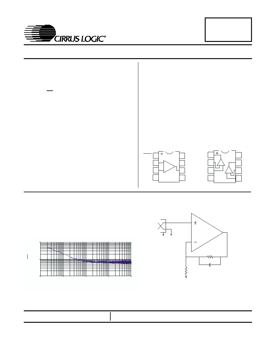
Pin Configurations
PWDN
-In
+In
V-
NC
V+
Output
NC
1
2
3
4
8
7
6
5
-
+
CS3001
8-lead SOIC
Out A
-In A
+In A
V-
V+
Out B
-In B
+In B
1
2
3
4
8
7
6
5
A
B
-
-
+
+
CS3002
8-lead SOIC
Noise vs. Frequency (Measured)
1
10
100
0.001
0.01
0.1
1
10
Frequency (Hz)
nV
/
Hz
CS3001
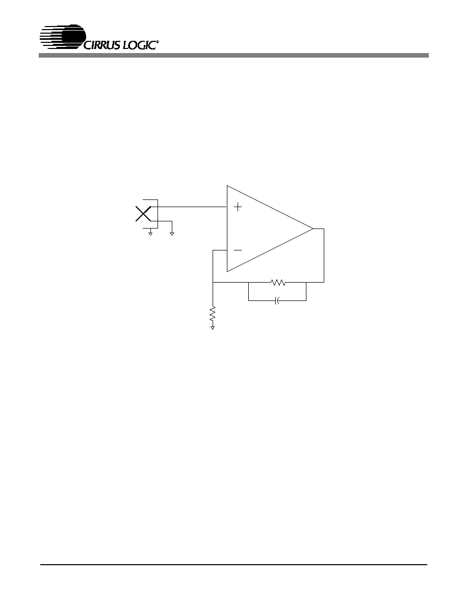
R1
100
R2
64.9k
C1
0.015
µ
µ
µ
µF
Dexter Research
Thermopile 1M
Thermopile Amplifier with a Gain of 650 V/V
OCT `02
DS490PP1
CS3001
CS3002
2
TABLE OF CONTENTS
1. CHARACTERISTICS AND SPECIFICATIONS ................................................... 3
1.1 Electrical Characteristics ...................................................................................... 3
1.2 Absolute Maximum Ratings ................................................................................. 4
2. PERFORMANCE PLOTS ......................................................................................... 4
3. CS3001/CS3002 OVERVIEW ................................................................................... 7
3.1 Open Loop Gain and Phase Response .................................................................. 7
3.2 Open Loop Gain and Stability Compensation ...................................................... 8
3.3 Powerdown (
PDWN) ......................................................................................... 10
3.4 Applications ........................................................................................................ 11
4. PACKAGE DRAWING ........................................................................................... 13
5. ORDERING INFORMATION ............................................................................... 14
LIST OF FIGURES
Figure 1. Noise vs Frequency (Measured) .........................................................................4
Figure 2. 0.01 Hz to 10 Hz Noise .......................................................................................4
Figure 3. Noise vs Frequency ............................................................................................4
Figure 4. Offset Voltage Stability (DC to 3.2 Hz) ...............................................................4
Figure 5. Open Loop Gain and Phase vs Frequency .........................................................5
Figure 6. Open Loop Gain and Phase vs Frequency (Expanded) .....................................5
Figure 7. Input Bias Current vs Supply Voltage (CS3002) .................................................6
Figure 8. Input Bias Current vs Common Mode Voltage ...................................................6
Figure 9. CS3001/CS3002 Open Loop Gain and Phase Response ..................................7
Figure 10. Non-Inverting Gain Configuration .....................................................................8
Figure 11. Non-Inverting Gain Configuration with Compensation ......................................9
Figure 12. Loop Gain Plot: Unity Gain and with Pole-Zero Compensation ......................10
Figure 13. Thermopile Amplifier with a Gain of 650 V/V ..................................................11
Figure 14. Load Cell Bridge Amplifier and A/D Converter ...............................................12
Contacting Cirrus Logic Support
For all product questions and inquiries contact a Cirrus Logic Sales Representative.
To find one nearest you go to <http://www.cirrus.com/corporate/contacts/sales.cfm>
IMPORTANT NOTICE
"Preliminary" product information describes products that are in production, but for which full characterization data is not yet available. "Advance" product infor-
mation describes products that are in development and subject to development changes. Cirrus Logic, Inc. and its subsidiaries ("Cirrus") believe that the infor-
mation contained in this document is accurate and reliable. However, the information is subject to change without notice and is provided "AS IS" without warranty
of any kind (express or implied). Customers are advised to obtain the latest version of relevant information to verify, before placing orders, that information being
relied on is current and complete. All products are sold subject to the terms and conditions of sale supplied at the time of order acknowledgment, including those
pertaining to warranty, patent infringement, and limitation of liability. No responsibility is assumed by Cirrus for the use of this information, including use of this
information as the basis for manufacture or sale of any items, or for infringement of patents or other rights of third parties. This document is the property of Cirrus
and by furnishing this information, Cirrus grants no license, express or implied under any patents, mask work rights, copyrights, trademarks, trade secrets or
other intellectual property rights. Cirrus owns the copyrights of the information contained herein and gives consent for copies to be made of the information only
for use within your organization with respect to Cirrus integrated circuits or other parts of Cirrus. This consent does not extend to other copying such as copying
for general distribution, advertising or promotional purposes, or for creating any work for resale.
An export permit needs to be obtained from the competent authorities of the Japanese Government if any of the products or technologies described in this ma-
terial and controlled under the "Foreign Exchange and Foreign Trade Law" is to be exported or taken out of Japan. An export license and/or quota needs to be
obtained from the competent authorities of the Chinese Government if any of the products or technologies described in this material is subject to the PRC Foreign
Trade Law and is to be exported or taken out of the PRC.
CERTAIN APPLICATIONS USING SEMICONDUCTOR PRODUCTS MAY INVOLVE POTENTIAL RISKS OF DEATH, PERSONAL INJURY, OR SEVERE
PROPERTY OR ENVIRONMENTAL DAMAGE ("CRITICAL APPLICATIONS"). CIRRUS PRODUCTS ARE NOT DESIGNED, AUTHORIZED, OR WARRANT-
ED TO BE SUITABLE FOR USE IN LIFE-SUPPORT DEVICES OR SYSTEMS OR OTHER CRITICAL APPLICATIONS. INCLUSION OF CIRRUS PRODUCTS
IN SUCH APPLICATIONS IS UNDERSTOOD TO BE FULLY AT THE CUSTOMER'S RISK.
Cirrus Logic, Cirrus, and the Cirrus Logic logo designs are trademarks of Cirrus Logic, Inc. All other brand and product names in this document may be trade-
marks or service marks of their respective owners.
CS3001
CS3002
3
1. CHARACTERISTICS AND SPECIFICATIONS
1.1
Electrical Characteristics
V+ = +5 V, V- = 0V, VCM = 2.5 V (
Note 1
)
Notes: 1. Symbol "∑" denotes specification applies over -40 to +85
∞
C.
2. This parameter is guaranteed by design and laboratory characterization. Thermocouple effects prohibit
accurate measurement of these parameters in automatic test systems.
3. 1000-hour life test data @ 125 ∞C indicates randomly distributed variation approximately equal to
measurement repeatability of 1 µV.
4. Measured within the specified common mode range limits.
5. Guaranteed within the output limits of (V+ -0.3 V) to (V- +0.3 V). Tested with proprietary production test
method.
6. PWDN input has an internal pullup resistor to V+ of approximately 800 k
and is the major source of
current consumption when PWDN is active low.
7. The device has a controlled start-up behavior due to its complex open loop gain characteristics. Start-
up time applies when supply voltage is applied or when PDWN is released.
Parameter
CS3001/CS3002
Unit
Min
Typ
Max
Input Offset Voltage
(
Note 2
)
∑
-
-
±10
µV
Average Input Offset Drift
(
Note 2
)
∑
-
±0.01
±0.05
µV/∫C
Long Term Input Offset Voltage Stability
(
Note 3
)
Input Bias Current
T
A
= 25∫ C
∑
-
±100
±200
±1000
pA
pA
Input Offset Current
T
A
= 25∫ C
∑
-
±200
±400
±2000
pA
pA
Input Noise Voltage Density R
S
= 100
, f
0
= 1 Hz
R
S
= 100
, f
0
= 1 kHz
-
-
6
6
Input Noise Voltage
0.1 to 10 Hz
-
125
nV
p-p
Input Noise Current Density f
0
= 1 Hz
-
2
Input Noise Current
0.1 to 10 Hz
-
40
pA
p-p
Input Common Mode Voltage Range
∑
-0.1
-
(V+)-1.25
V
Common Mode Rejection Ratio (dc)
(
Note 4
)
∑
115
120
-
dB
Power Supply Rejection Ratio
∑
120
136
-
dB
Large Signal Voltage Gain R
L
= 2 k
to V+/2
(
Note 5
)
∑
200
300
-
dB
Output Voltage Swing
R
L
= 2 k
to V+/2
R
L
= 100 k
to V+/2
∑
+4.7
-
+4.99
-
V
V
Slew Rate
R
L
= 2 k, 100 pF
5
-
V/µs
Overload Recovery Time
-
100
-
µs
Supply Current per Amplifier
PWDN active (CS3001 Only)
(
Note 6
)
∑
∑
-
1.8
2.4
15
mA
µA
PWDN Threshold
(
Note 6
)
∑
(V+) -1.0
-
-
V
Start-up Time
(
Note 7
)
∑
-
9
12
ms
nV/ Hz
nV/ Hz
pA/ Hz
CS3001
CS3002
4
1.2
Absolute Maximum Ratings
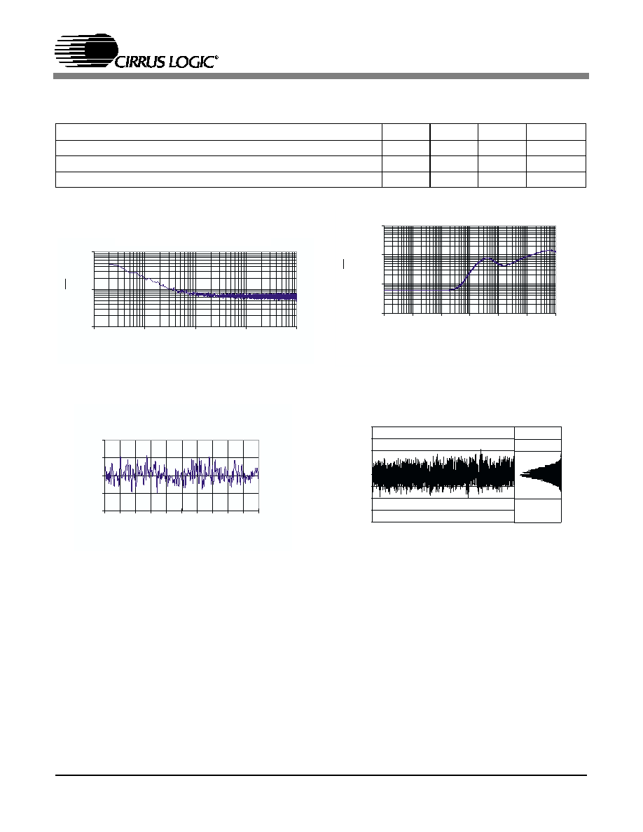
2. PERFORMANCE PLOTS
Parameter
Min
Typ
Max
Unit
Supply Voltage
[(V+) - (V-)]
6.8
V
Input Voltage
V- -0.3
V+ +0.3
V
Storage Temperature Range
-65
+150
∫C
Noise vs. Frequency (Measured)
1
10
100
0.001
0.01
0.1
1
10
Frequency (Hz)
nV
/
Hz
Figure 1. Noise vs Frequency (Measured)
-100
-50
0
50
100
TIM E (Sec)
n
V
0
1
2
3
4
5
6
7
8
9
10
Figure 2. 0.01 Hz to 10 Hz Noise
1
10
100
1000
10
100
1K
10K
100K
1M
10M
Frequency (Hz)
nV
/
Hz
Figure 3. Noise vs Frequency
Time (1 Hour)
-100
-75
-50
-25
0
25
50
75
100
nV
= 13 nV
Figure 4. Offset Voltage Stability (DC to 3.2 Hz)
CS3001
CS3002
5
Performance Plots (Cont.)
-500
-400
-300
-200
-100
0
100
200
300
400
500
1
10
100
1K
10K
100K
1M
10M
Frequency (Hz)
Ga
in
(
d
B
)
P
h
ase
(
D
e
gr
ees)
Gain
Phase
Figure 5. Open Loop Gain and Phase vs Frequency
-360
-315
-270
-225
-180
-135
-90
-45
10K
100K
1M
10M
Gain (dB)
Phase (Degrees)
0
20
40
60
80
100
Figure 6. Open Loop Gain and Phase vs Frequency (Expanded)

CS3001
CS3002
6
Performance Plots (Cont.)
Supply Voltage (±V)
Input Bias Current (pA)
A1-
A1+
B1-
A2+
B1+
A2-
B2-
B2+
±1.35
±2
±2.5
±3.35
-200
-150
-150
-100
-100
0
-50
-50
CM = 0 V
Figure 7. Input Bias Current vs Supply Voltage (CS3002)
-3
-2
-1
0
1
2
3
0
1
2
3
4
5
Common Mode Voltage (Vs = 5V)
Bias Current Normalized to CM = 2.5 V
Figure 8. Input Bias Current vs Common Mode Voltage

CS3001
CS3002
7
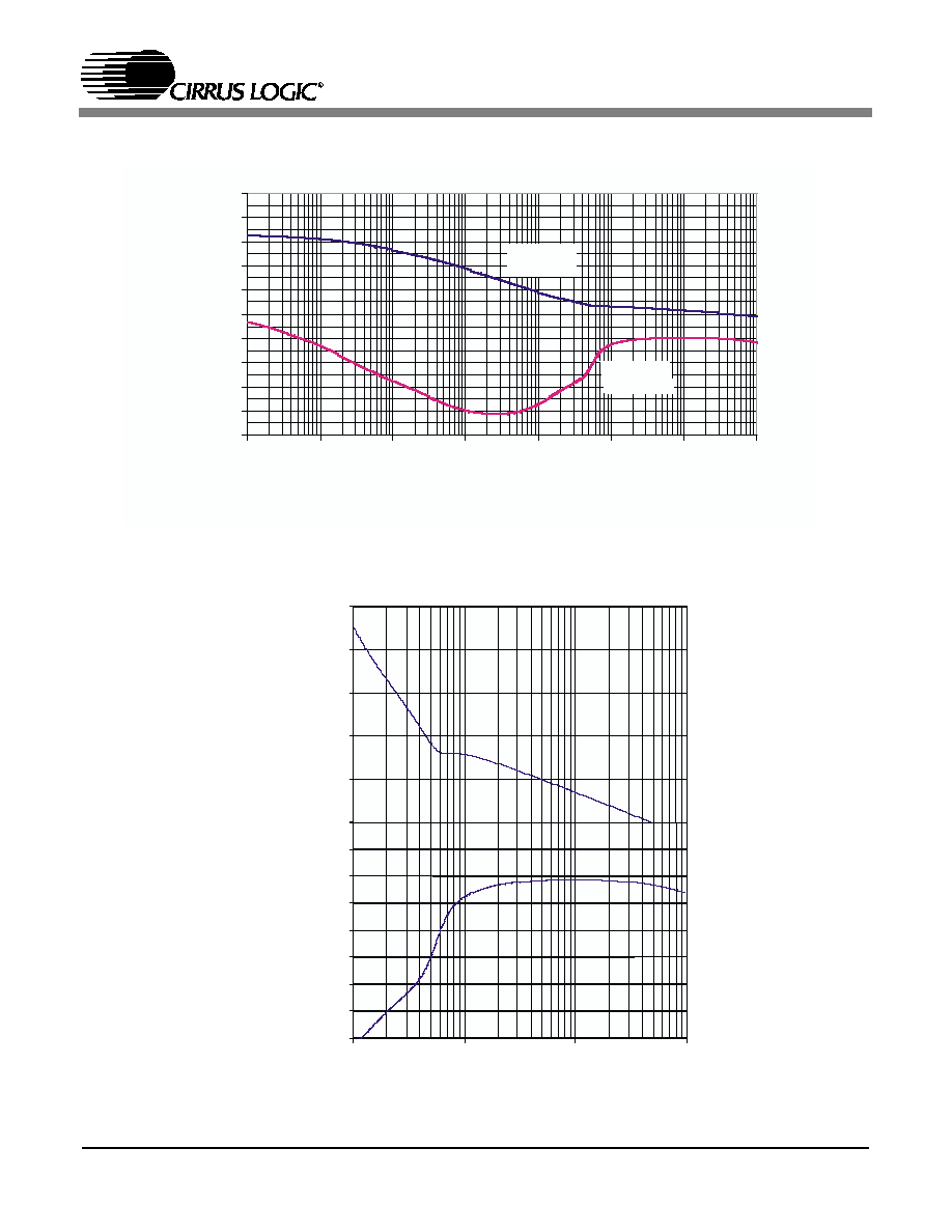
3. CS3001/CS3002 OVERVIEW
The CS3001/CS3002 amplifiers are designed for
precision measurement of signals from DC to
2 kHz when operating from a supply voltage of
+2.7 V to +6.7 V (
± 1.35 to ± 3.35 V). The ampli-
fiers are designed with a patented architecture that
utilizes multiple amplifier stages to yield very high
open loop gain at frequencies of 10 kHz and below.
The amplifiers yield low noise and low offset drift
while consuming relatively low supply current. An
increase in noise floor above 2 kHz is the result of
intermediate stages of the amplifier being operated
at very low currents. The amplifiers are intended
for amplifying small signals with large gains in ap-
plications where the output of the amplifier can be
band-limited to frequencies below 2 kHz.
3.1
Open Loop Gain and Phase
Response
Figure 9
illustrates the open loop gain and phase re-
sponse of the CS3001/CS3002. The gain slope of
the amplifier is about ≠100 dB/decade between
500 Hz and 60 kHz and transitions to ≠20 dB/de-
cade between 60 kHz and its unity gain crossover
frequency at about 4.8 MHz. Phase margin at unity
gain is about 70 degrees; gain margin is about
20 dB.
-360
-315
-270
-225
-180
-135
-90
-45
10K
100K
1M
10M
Gain (dB)
Phase (Degrees)
0
20
40
60
80
100
-100 dB/ dec
-20 dB/ dec
Figure 9. CS3001/CS3002 Open Loop Gain and Phase Response
CS3001
CS3002
8
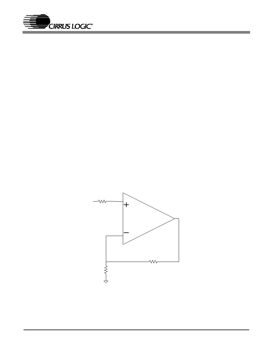
3.2
Open Loop Gain and Stability
Compensation
The CS3001 and CS3002 achieve ultra-high open
loop gain.
Figure 10
illustrates the amplifier in a
non-inverting gain configuration. The open loop
gain and phase plots indicate that the amplifier is
stable for closed-loop gains less than 50 V/V. For a
gain of 50, the phase margin is between 40
∞ and 60∞
depending upon the loading conditions. As shown
in
Figure 11 on page 9
, the op amp has an input ca-
pacitance at the + and ≠ signal inputs of typically
50 pF. This capacitance adds an additional pole in
the loop gain transfer function at a frequency of
f = 1/(2
R*C
in
) where R is the parallel combina-
tion of R1 and R2 (R1
|| R2). A higher value for R
produces a pole at a lower frequency, thus reducing
the phase margin. R1 is recommended to be less
than or equal to 100 ohms, which results in a pole
at 30 MHz or higher. If a higher value of R1 is de-
sired, a compensation capacitor (C2) should be
added in parallel with R2. C2 should be chosen
such that R2*C2
R1*C
in
.
R 1
R 2
V in
V o
R
S
Figure 10. Non-Inverting Gain Configuration
CS3001
CS3002
9
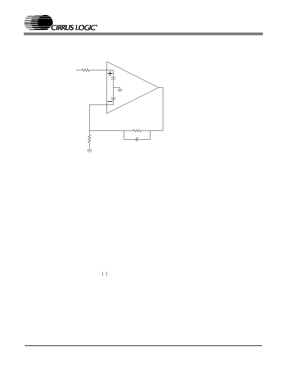
The feedback capacitor C2 is required for closed-
loop gains greater than 50 V/V. The capacitor in-
troduces a pole and a zero in the loop gain transfer
function,
This indicates that the separation of the pole and
the zero is governed by the closed loop gain. It is
required that the zero falls on the steep slope
(≠100 dB/decade) of the loop gain plot so that there
is some gain higher than 0 dB (typically 20 dB) at
the hand-over frequency (the frequency at which
the slope changes from ≠ 100 dB/decade to
≠20 dB/decade).
5 0 p F
5 0 p F
R 1
R 2
V in
V o
C 2
C
in
C
in
C h o o s e C 2
so th at R 2C 2
R 1 C
in
Figure 11. Non-Inverting Gain Configuration with Compensation
T
1
s
z
1
-----
+
≠
1
s
p
1
-----
+
-----------------------A
ol
=
P
1
1
2
R
1
R
2
||
(
)C
2
-------------------------------------
1
2
R
1
C
2
(
)
-------------------------
=
for
R
2
R
1
ª
Z
1
1
2
A R
1
◊
(
)C
2
-----------------------------------
=
where
A
R
2
R
1
------
=
CS3001
CS3002
10
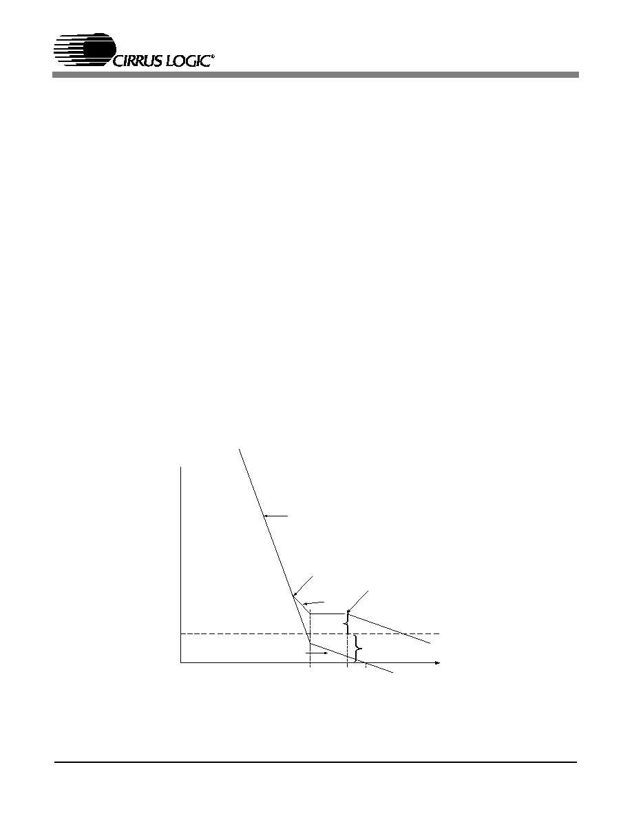
The loop gain plot shown in
Figure 12
illustrates
the unity gain configuration, and indicates how this
is modified when using the amplifier in a higher
gain configuration with compensation. If it is con-
figured for higher gain, for example, 60 dB, the
x≠axis will move up by 60 dB (line B). Capacitor
C2 adds a zero and a pole. The modified plot indi-
cates the effects of introducing the pole and zero
due to capacitor C2. The pole can be located at any
frequency higher than the hand-over frequency, the
zero has to be at a frequency lower than the hand-
over frequency so as to provide adequate gain mar-
gin. The separation between the pole and the zero
is governed by the closed loop gain. The zero (z
1
)
occurs at the intersection of the ≠100 dB/decade
and ≠80 dB/decade slopes. The point X in the fig-
ure should be at closed loop gain plus 20 dB gain
margin.
The value for C2 = 1/(2
R1p1). Using
p1 = 1 MHz works very well and is independent of
gain. As the closed loop gain is changed, the zero
location is also modified if R1 remains fixed.
Capacitor C2 can be increased in value to limit the
amplifier's rising noise above 2 kHz.
3.3
Powerdown (
PDWN)
The CS3001 single amplifier provides a power-
down function on pin 1. If this pin is left open the
amplifier will operate normally. If the powerdown
is asserted low, the amplifier will go into a low
power state. There is a pull-up resistor (approxi-
mately 800 k ohm) inside the amplifier from pin
1 to the V+ supply. The current through this pull-up
resistor is the main source of current drain in the
powerdown state.
3.4
Applications
The CS3001 and CS3002 amplifiers are optimum
for applications that require high gain and low drift.
Figure 13
illustrates a thermopile amplifier with a
gain of 650 V/V. The thermopile outputs only a few
millivolts when subjected to infrared radiation. The
amplifier is compensated and bandlimited by C1 in
combination with R2.
-100 dB/dec
|T| (Log gain)
-80 dB/dec
z
1
p
1
Margin
-20 dB/dec
50kHz
1MHz
5MHz
Desired Closed
Loop Gain
X
FREQUENCY
B
Figure 12. Loop Gain Plot: Unity Gain and with Pole-Zero Compensation
CS3001
CS3002
11
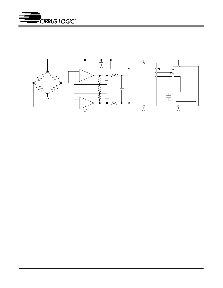
Figure 14 on page 12
illustrates a load cell bridge
amplifier with a gain of 768 V/V. The load cell is
excited with +5 V and has a 1 mV/V sensitivity. Its
full scale output signal is amplified to produce a
fully differential
± 3.8 V into the CS5510/12 A/D
converter. This circuit operates from +5 V.
A similar circuit operating from +3 V can be
constructed using the CS5540/CS5541 A/D con-
verters.
C S 3 00 1
R 1
10 0
R 2
6 4 .9k
C 1
0 .0 1 5
µ
µ
µ
µ F
D exter Research
Therm opile 1M
T h e rm o p ile A m p lifie r w ith a G ain o f 65 0 V /V
Figure 13. Thermopile Amplifier with a Gain of 650 V/V
CS3001
CS3002
12
+ 5 V
V A
1 m V /V
-
+
3 5 0
+
-
-
+
x 7 6 8
1 4 0 k
3 6 5
1 4 0 k
1 0 0
1 0 0
0 .2 2
µ F
0 .2 2
µ F
0 .0 4 7
µ F
0 .1
µ F
V R E F
A IN +
A IN 1
V -
V +
C S
S D O
S C L K
C S 5 5 1 0 /1 2
µ
µ
µ
µ
+ 5 V
+ 5 V
C o u n te r /T im e r
S C L K = 1 0 k H z to 1 0 0
k H
(3 2 .7 6 8
i
l )
S C L K = 1 0 k H z t o 1 0 0 k H z
( 3 2 . 7 6 8 n o m i n a l
)
Figure 14. Load Cell Bridge Amplifier and A/D Converter
CS3001
CS3002
13
4. PACKAGE DRAWING
INCHES
MILLIMETERS
DIM
MIN
MAX
MIN
MAX
A
0.053
0.069
1.35
1.75
A1
0.004
0.010
0.10
0.25
B
0.013
0.020
0.33
0.51
C
0.007
0.010
0.19
0.25
D
0.189
0.197
4.80
5.00
E
0.150
0.157
3.80
4.00
e
0.040
0.060
1.02
1.52
H
0.228
0.244
5.80
6.20
L
0.016
0.050
0.40
1.27
0∞
8∞
0∞
8∞
JEDEC # : MS-012
8L SOIC (150 MIL BODY) PACKAGE DRAWING
D
H
E
e
b
A1
A
c
L
SEATING
PLANE
1
CS3001
CS3002
14
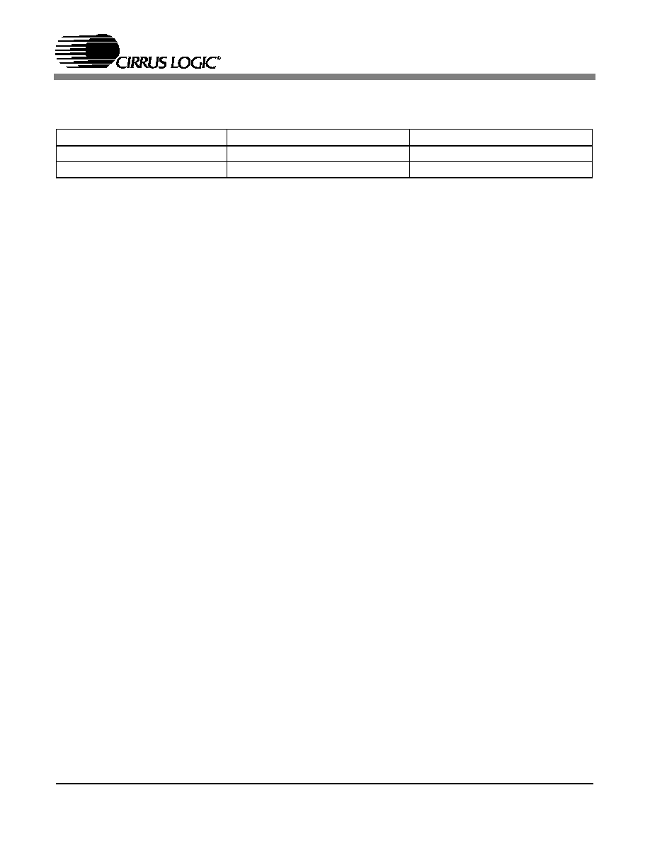
5. ORDERING INFORMATION
Part #
Temperature Range
Package Description
CS3001-IS
-40 ∞C to +85 ∞C
8-lead SOIC
CS3002-IS
-40 ∞C to +85 ∞C
8-lead SOIC
Note: Add the letter R to the Part # to order reels. There are 2000 pieces per reel.

∑ Notes ∑
