 | –≠–ª–µ–∫—Ç—Ä–æ–Ω–Ω—ã–π –∫–æ–º–ø–æ–Ω–µ–Ω—Ç: CS3310-KS | –°–∫–∞—á–∞—Ç—å:  PDF PDF  ZIP ZIP |
Document Outline
- CS3310: Stereo Digital Volume Control
- Features
- Description
- ORDERING INFORMATION
- Characterisics & Specifications
- ANALOG CHARACTERISTICS
- DIGITAL CHARACTERISTICS
- SWITCHING CHARACTERISTICS
- Figure 1. Serial Port Timing Diagram
- RECOMMENDED OPERATING CONDITIONS
- ABSOLUTE MAXIMUM RATINGS
- Figure 2. Recommended Connection Diagram
- GENERAL DESCRIPTION
- SYSTEM DESIGN
- Table 1. Input Code Definition
- Serial Data Interface
- Figure 3. Serial Port Timing
- Daisy Chaining
- Figure 4. Daisy Chaining Diagram
- Changing the Analog Output Level
- Analog Inputs and Outputs
- Source Impedance Requirements
- Mute
- Power-Up Considerations
- PCB Layout, Grounding and Power Supply Decoupling
- Figure 5. Recommended 2-Layer PCB Layout
- Performance Plots
- Figure 6. THD+N vs. AMP
- Figure 7. 20 kHz Crosstalk
- Figure 8. Frequency Response Full Scale Input
- Figure 9. Frequency Response -20 dB Input
- Figure 10. THD+N vs. Frequency LOAD = 600 W, 2 kW, open ckt
- Figure 11. THD+N vs. Frequency Output levels of 1, 2, and 2.8 Vrms
- PIN DESCRIPTION
- Pin Layout Drawing
- Power Supply Connections
- Analog Inputs and Outputs
- Digital Pins
- PARAMETER DEFINITIONS
- PACKAGE DIMENSIONS
- 16 PIN PLASTIC (PDIP) PACKAGE DRAWING
- 16L SOIC (300 MIL BODY) PACKAGE DRAWING
- CDB3310: Evaluation Board for CS3310
Preliminary Product Information
This document contains information for a new product.
Cirrus Logic reserves the right to modify this product without notice.
1
Copyright
©
Cirrus Logic, Inc. 1999
(All Rights Reserved)
Products from
P.O. Box 17847, Austin, Texas 78760
(512) 445 7222 FAX: (512) 445 7581
http://www.crystal.com
CS3310
Stereo Digital Volume Control
Features
l
Complete Digital Volume Control
-- 2 Independent Channels
-- Serial Control
-- 0.5 dB Step Size
l
Wide Adjustable Range
-- -95.5 dB Attenuation
-- +31.5 dB Gain
l
Low Distortion & Noise
-- 0.001% THD+N
-- 116 dB Dynamic Range
l
Noise Free Level Transitions
l
Channel-to-Channel Crosstalk Better Than
110 dB
Description
The CS3310 is a complete stereo digital volume control
designed specifically for audio systems. It features a 16-
bit serial interface that controls two independent, low dis-
tortion audio channels.
The CS3310 includes an array of well-matched resistors
and a low noise active output stage that is capable of
driving a 600
load. A total adjustable range of 127 dB,
in 0.5 dB steps, is achieved through 95.5 dB of attenua-
tion and 31.5 dB of gain.
The simple 3-wire interface provides daisy-chaining of
multiple CS3310's for multi-channel audio systems.
The device operates from ±5 V supplies and has an in-
put/output voltage range of ±3.75 V.
ORDERING INFORMATION
CS3310-KP
0∞ to 70∞ C
16-pin Plastic DIP
CS3310-KS
0∞ to 70∞ C
16-pin Plastic SOIC
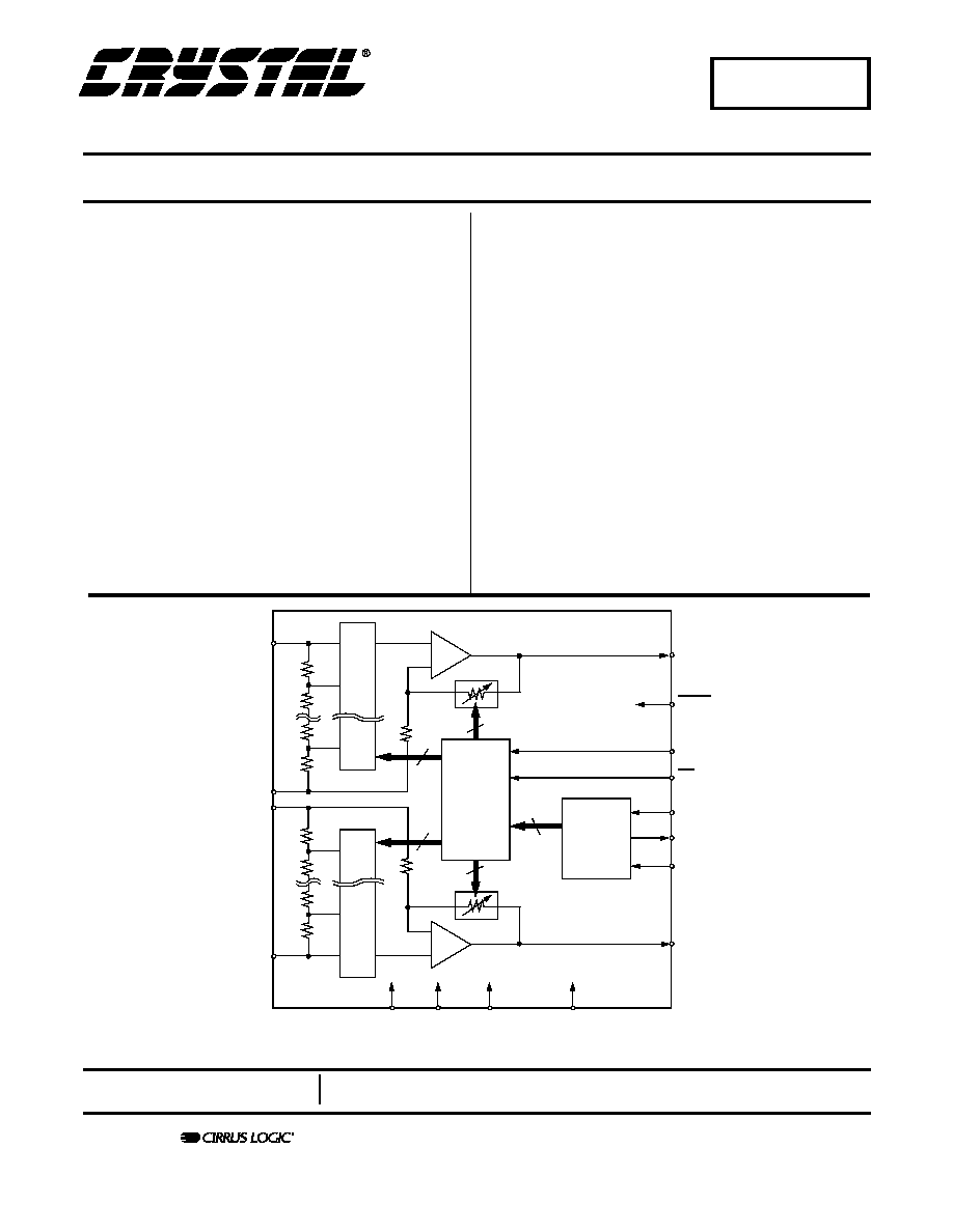
I
AINL
AGNDL
MUX
AINR
AGNDR
MUX
16
15
10
9
8
8
+
-
+
-
Control
Register
Serial to
Parallel
Register
16
8
8
AOUTL
14
MUTE
8
1
2
ZCEN
CS
3
SDATAI
7
SDATAO
6
SCLK
AOUTR
11
DGND
5
VD+
4
VA-
13
VA+
12
FEB `99
DS82PP3

CS3310
2
DS82PP3
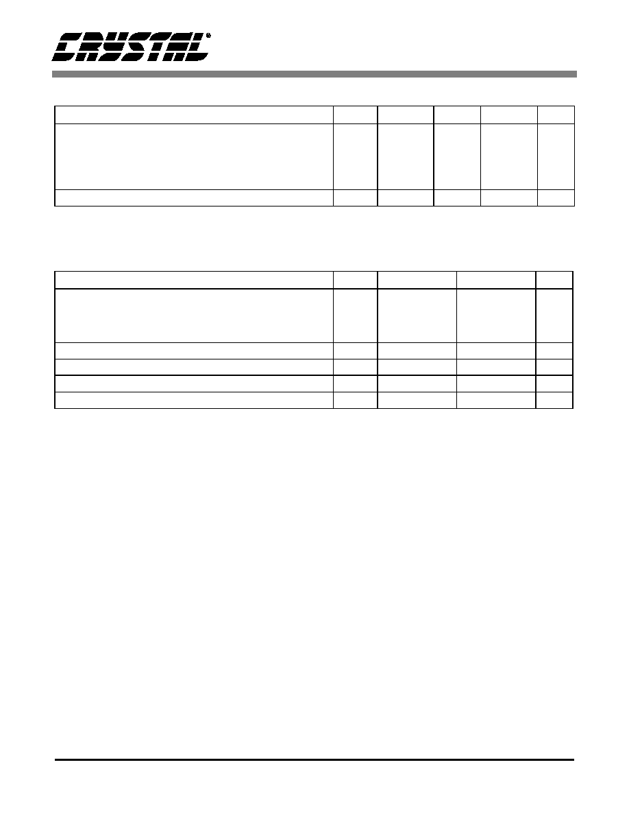
ANALOG CHARACTERISTICS
(T
A
= 25 ∞C, VA+, VD+ = 5 V ± 5%; VA- = -5V ± 5%; Rs = 0; R
L
=
2 k
; C
L
= 20 pF; 10 Hz to 20 kHz Measurement Bandwidth; unless otherwise specified)
Notes: 1. Measured with input grounded and Gain = 1. Will increase as a function of Gain settings >1.
2. This parameter is guaranteed by design and/or characterization.
Parameter
Symbol Min
Typ
Max
Unit
DC Characteristics
Step Size
-
0.5
-
dB
Gain Error (31.5 dB Gain)
-
±
0.05
-
dB
Gain Matching Between Channels
-
±
0.05
-
dB
Input Resistance
R
IN
8
10
-
k
Input Capacitance
C
IN
-
10
-
pF
AC Characteristics
Total Harmonic Distortion plus Noise (V in = 2V rms, 1 kHz)
THD+N
-
0.001
.0025
%
Dynamic Range
110
116
-
dB
Input/Output Voltage Range
(VA-)+1.25
-
(VA+)-1.25
V
Output Noise
(Note 1)
-
4.2
8.4
µ
Vrms
Digital Feedthrough (Peak Component)
(Note 2)
-80
-
-
dB
Interchannel Isolation (1 kHz)
(Note 2)
-100
-110
-
dB
Output Buffer
Offset Voltage
(Note 1)
V
OS
-
0.25
0.75
mV
Load Capacitance
-
-
100
pF
Short Circuit Current
-
20
-
mA
Unity Gain Bandwidth, Small Signal
(Note 2)
2
-
-
MHz
Power Supplies
Supply Current (No Load, AIN = 0 V)
IA+
IA-
ID+
-
-
-
5.0
5.0
350
8.0
8.0
800
mA
mA
µ
A
Power Consumption
P
D
-
52.0
84.0
mW
Power Supply Rejection Ratio (250 Hz)
PSRR
-
80
-
dB

CS3310
DS82PP3
3
DIGITAL CHARACTERISTICS
(T
A
= 25 ∞C, VA+ , VD+ = 5V ± 5%, VA- = -5V ± 5% )
SWITCHING CHARACTERISTICS
(T
A
= 25 ∞C; VA+, VD+ = +5V ± 5%; VA- = -5V ± 5%; C
L
= 20 pF)
Parameter
Symbol Min
Typ
Max
Unit
High-Level Input Voltage
V
IH
2.0
-
VD+0.3
V
Low-Level Input Voltage
V
IL
-0.3
-
+0.8
V
High-Level Output Voltage
(I
O
= 200
µ
A)
V
OH
VD-1.0
-
-
V
Low-Level Output Voltage
(I
O
= 3.2mA)
V
OL
-
-
0.4
V
Input Leakage Current
I
in
-
1.0
10
µ
A
Parameter
Symbol Min
Typ
Max
Unit
Serial Clock
SCLK
0
-
-
MHz
Serial Clock
Pulse Width High
Pulse Width Low
t
ph
t
pl
80
80
-
-
-
-
ns
ns
MUTE Pulse
Width
Low
-
2.0
-
-
ms
Input Timing
SDATAI Set Up Time
t
SDVS
20
-
-
ns
SDATAI Hold Time
t
SDH
20
-
-
ns
CS Valid to SCLK Rising
t
CSVS
30
-
-
ns
SCLK Falling to CS High
t
LTH
35
-
-
ns
Output Timing
CS Low to Output Active
t
CSH
-
-
35
ns
SCLK Falling to Data Valid
t
SSD
-
-
60
ns
CS High to SDATAO Inactive
t
CSDH
-
-
100
ns
t CSVS
t SDVS
tSDH
SCLK
SDATAI
CS
SDATAO
t CSH
tCSDH
t SSD
MSB
tLTH
Figure 1. Serial Port Timing Diagram
CS3310
4
DS82PP3
RECOMMENDED OPERATING CONDITIONS
(DGND = 0V; all voltages with respect to ground)
Notes: 3. Applying power to VD+ prior to VA+ creates a SCR latch-up condition. Refer to Figure 2 for the
recommended power connections.
ABSOLUTE MAXIMUM RATINGS
(AGND, DGND = 0V, all voltages with respect to ground.)
Parameter
Symbol Min
Typ
Max
Unit
DC Power Supplies:
Positive Digital
Positive Analog
Negative Analog
(VD+) - (VA+) (Note 3)
VD+
VA+
VA
-
4.75
4.75
-4.75
-0.3
5.0
5.0
-5.0
-
VA+
5.25
-5.25
0.0
V
V
V
V
Ambient Operating Temperature
T
A
0
25
70
∞
C
Parameter
Symbol Min
Max
Unit
DC Power Supplies:
Positive Digital
Positive Analog
Negative Analog
VD+
VA+
VA-
-0.3
-0.3
0.3
(VA+)+ 0.3
6.0
-6.0
V
V
V
Input Current, Any Pin Except Supply
I
in
-
±
10
mA
Digital Input Voltage
V
IND
-0.3
(VA+) + 0.3
V
Ambient Operating Temperature (power applied)
T
A
-55
+125
∞
C
Storage Temperature
T
STG
-65
+150
∞
C

CS3310
DS82PP3
5
CS3310
AINL
AINR
AGNDL
AGNDR
VD+
VA+
VA-
SDATAO
CS
SDATAI
TO ANOTHER
CS3310 OR
CONTROLLER
CONTROLLER
SCLK
AUDIO
SOURCE
AOUTL
AOUTR
7
10
11
12
13
14
15
+
+
+5V ANALOG
-5V ANALOG
2
3
6
16
9
DGND
5
AUDIO
OUTPUTS
4
ZCEN
0.1
µ
F
10
µ
F
+
10
1
MUTE
8
0.1
µ
F
10
µ
F
0.1
µ
F
0.1
µ
F
10
µ
F
47 k
Figure 2. Recommended Connection Diagram
*Required to terminate SDATAI due to high impedance
state of SDATAO when CS is high.
**Refer to Note 3.
*
**