 | –≠–ª–µ–∫—Ç—Ä–æ–Ω–Ω—ã–π –∫–æ–º–ø–æ–Ω–µ–Ω—Ç: CS4218-KQ | –°–∫–∞—á–∞—Ç—å:  PDF PDF  ZIP ZIP |
Complete CMOS Stereo Audio Input
and Output System featuring:
∑
Delta-Sigma A/D and D/A Converters using
64x Oversampling.
∑
Input Anti-Aliasing and Output Smoothing
Filters.
∑
Programmable Input Gain (0 dB to 22.5 dB).
∑
Programmable Output Attenuation (0 dB to
46.5 dB).
∑
Sample frequencies from 4 kHz to 50 kHz.
∑
Low Distortion, THD < 0.02% for DAC.
THD < 0.02% for ADC.
∑
Low Power Dissipation: 80 mA typical.
∑
Power-Down Mode : 1 mA typical.
∑
Pin Compatible with CS4216 when used in
Serial Modes 3 and 4 (See Appendix A).
∑
I
2
S(TM) Compatible Serial Mode (SM5).
∑
Operates from 5V or 3.3V Digital Power
Supply. Requires 5V Analog Power Supply.
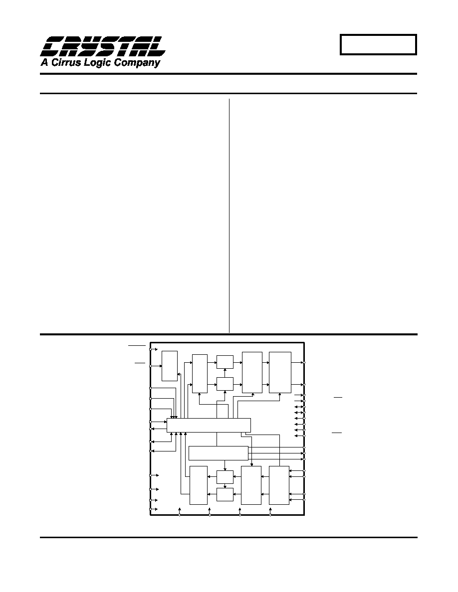
General Description
The CS4218 Stereo Audio Codec is a monolithic
CMOS device for computer multimedia, automotive,
and portable audio applications. It performs A/D and
D/A conversion, filtering, and level setting, creating 4
audio inputs and 2 audio outputs for a digital computer
system. The digital interfaces of left and right channels
are multiplexed into a single serial data bus with word
rates up to 50 kHz per channel.
ADCs and the DACs use delta-sigma modulation with
64X oversampling. The ADCs and DACs include digi-
tal decimation filters and output smoothing filters
on-chip which eliminate the need for external anti-alias-
ing filters.
The CS4218 is pin and function compatible with the
CS4216 when used in Serial modes 3 and 4. See the
Appendix A at the end of this data sheet for details.
I
2
S is a trademark of Philips.
Ordering Information:
CS4218-KL
0
∞
to 70
∞
C
44-pin PLCC
CS4218-KQ
0
∞
to 70
∞
C
44-pin TQFP
16-Bit Stereo Audio Codec
CS4218
SSYNC
LOUT
ROUT
DI
GI
T
A
L
FIL
T
ER
S
SERIAL INTERFACE CONTROL
DI
GI
T
A
L
FIL
T
ER
S
INPUT
MUX
VOLTAGE REFERENCE
CLKIN
MF7:SFS1/F2
MF8:SFS2/F3
SDIN
SDOUT
SCLK
SMODE1
RESET
REFGND
REFBYP
REFBUF
LIN1
LIN2
RIN1
RIN2
VD
VA
DGND
AGND
A/D
A/D
D/A
D/A
DO1
MF5:DO2/INT
MF2:F2/CDIN
MF1:F1/CDOUT
DI1
MF6:DI2/F1
MF3:DI3/F3/CCLK
OUTPUT
MUTE
OUT
P
UT
A
TTE
N
U
ATIO
N
INPUT
GAIN
PDN
SMODE2
SMODE3
PO
W
E
R
CO
N
T
RO
L
FILT
MF4:MA/CCS
SEP '96
DS135F1
1
Crystal Semiconductor Corporation
P.O. Box 17847, Austin, TX 78760
(512) 445 7222 FAX: (512) 445 7581
http://www.crystal.com
Copyright
©
Crystal Semiconductor Corporation 1996
(All Rights Reserved)

Contents
Description
Cover . . . . . . . . . . . . . . . . . . . .
1
Contents
. . . . . . . . . . . . . . . . . . .
2
Recommended Operating Conditions . . . . . . . . . . . .
3
Analog Input Characteristics . . . . . . . . . . . . . .
3
Analog Output Characteristics
. . . . . . . . . . . . .
4
Switching Characteristics . . . . . . . . . . . . . . .
5
Digital Characteristics . . . . . . . . . . . . . . . .
7
A/D Decimation Filter Characteristics . . . . . . . . . . . .
8
D/A Interpolation Characteristics . . . . . . . . . . . . .
8
Absolute Maximum Ratings
. . . . . . . . . . . . . .
8
Filter Response Plots . . . . . . . . . . . . . . . .
9
Typical Connection Diagram . . . . . . . . . . . . . .
11
Overview . . . . . . . . . . . . . . . . . . .
12
Functional Description
. . . . . . . . . . . . . . .
12
- Analog Inputs and Outputs . . . . . . . . . . . . .
12
- Offset Calibration
. . . . . . . . . . . . . . .
13
- Input Gain and Output Level Setting
. . . . . . . . . .
13
- Muting and the ADC Valid Counter . . . . . . . . . . .
13
- Parallel Digital I/O Pins . . . . . . . . . . . . . .
13
- Reset and Power Down Modes . . . . . . . . . . . .
13
- Audio Serial Interface
. . . . . . . . . . . . . .
14
Serial Interface Modes
. . . . . . . . . . . . . . .
15
- Serial Mode 3
. . . . . . . . . . . . . . . .
15
- Serial Mode 4
. . . . . . . . . . . . . . . .
22
- Serial Mode 5
. . . . . . . . . . . . . . . .
25
Power Supply and Grounding . . . . . . . . . . . . . .
26
Pin Diagrams and Descriptions
. . . . . . . . . . . . .
29
Package Information . . . . . . . . . . . . . . . .
35
Parameter Definitions . . . . . . . . . . . . . . . .
36
Appendix A: CS4218 Compatibility with the CS4216 . . . . . . . .
38
Appendix B: Applications of Serial Mode 4 (SM4)
. . . . . . . .
40
Appendix C: Setting CLKIN/SCLK Ratio for Desired Sample Rate . . . .
43
CS4218
2
DS135F1
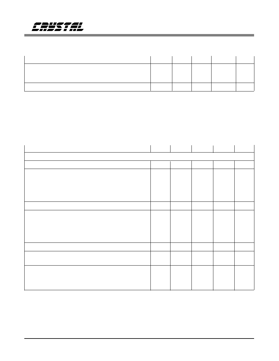
ANALOG CHARACTERISTICS
( T
A
= 25
∞
C; VA, VD = +5V; Input Levels: Logic 0 = 0V,
Logic 1 = VD; 1kHz Input Sine Wave; CLKIN = 12.288 MHz; SM3 Slave sub-mode, 256 BPF; 0dB gain/attenu-
ation;Conversion Rate = 48 kHz; SCLK = 12.288 MHz; Measurement Bandwidth is 10 Hz to 20 kHz; Unless oth-
erwise specified.)
Parameter *
Symbol
Min
Typ
Max
Units
Analog Input Characteristics - Minimum gain setting (0 dB); unless otherwise specified.
ADC Resolution
16
-
-
Bits
ADC Differential Nonlinearity
(Note 1)
-
-
±
0.9
LSB
Instantaneous Dynamic Range
(Note 3)
IDR
80
84
-
dB
Total Harmonic Distortion
THD
-
-
0.02
%
Interchannel Isolation
-
80
-
dB
Interchannel Gain Mismatch
-
-
±
0.5
dB
Frequency Response
(Note 1)
-0.5
-
+0.2
dB
Programmable Input Gain
-
22.5
-
dB
Gain Step Size
-
1.5
-
dB
Absolute Gain Step Error
-
-
0.75
dB
Gain Drift
(Note 1)
-
100
-
ppm/
∞
C
Offset Error
0dB Gain
-
-
±
50
LSB
22.5dB Gain
-
-
±
500
LSB
Full Scale Input Voltage
2.5
2.8
3.1
Vpp
Input Resistance
(Notes 1,2)
20
-
-
k
Input Capacitance
(Note 1)
-
-
15
pF
Notes:
1. This specification is guaranteed by characterization, not production testing.
2. Input resistance is for the input selected. Non-selected inputs have a very high (>1M
) input resistance.
3. Operation in Slave sub-modes may yield results lower than the 80 dB minimum.
* Parameter definitions are given at the end of this data sheet.
Specifications are subject to change without notice.
RECOMMENDED OPERATING CONDITIONS
(AGND, DGND = 0V, all voltages with respect
to 0V.)
Parameter
Symbol
Min
Typ
Max
Units
Power Supplies:
Digital
VD
4.75
5.0
5.25
V
Digital (Low Voltage)
VD
3.0
3.3
3.6
V
Analog
VA
4.75
5.0
5.25
V
Operating Ambient Temperature
TA
0
25
70
∞
C
CS4218
DS135F1
3
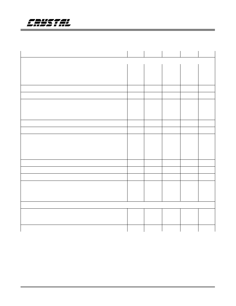
ANALOG CHARACTERISTICS
(Continued)
Parameter *
Symbol
Min
Typ
Max
Units
Analog Output Characteristics - Minimum Attenuation; Unless Otherwise Specified.
DAC Resolution
16
-
-
Bits
DAC Differential Nonlinearity
(Note 1)
-
-
±
0.9
LSB
Total Dynamic Range
TDR
-
93
-
dB
Instantaneous Dynamic Range
IDR
80
83
-
dB
Total Harmonic Distortion
(Note 4)
THD
-
-
0.02
%
Interchannel Isolation
(Note 4)
-
80
-
dB
Interchannel Gain Mismatch
-
-
±
0.5
dB
Frequency Response
(Note 1)
-0.5
-
+0.2
dB
Programmable Attenuation
(Note 5)
-
-46.5
-
dB
Attenuation Step Size
(Note 5)
-
1.5
-
dB
Absolute Attenuation Step Error
(Note 5)
-
-
0.75
dB
Gain Drift
(Note 1)
-
100
-
ppm/
∞
C
REFBUF Output Voltage
(Note 6)
1.9
2.1
2.3
V
Maximum output current= 400
µ
A
Offset Voltage
(Note 7)
-
10
-
mV
Full Scale Output Voltage
(Note 4)
2.4
2.7
3.1
Vpp
External Load Impedance
10k
-
-
Internal Resistor Value for LOUT and ROUT
400
600
800
Deviation from Linear Phase
(Note 1)
-
-
1
Degree
Out of Band Energy
(22 kHz to 100 kHz)
-
-60
-
dB
Power Supply
Power Supply Current
(Note 8)
Operating (VD = 5.0V)
-
80
100
mA
Operating (VD = 3.3V)
-
65
85
mA
Power Down
-
-
1
mA
Power Supply Rejection
(1 kHz)
-
40
-
dB
Notes:
4. 10 k
, 100 pF load.
5. Tested in SM3, Slave sub-mode, 256 BPF.
6. REFBUF load current must be DC. To drive dynamic loads, REFBUF must be buffered.
AC variations in REFBUF current may degrade ADC and DAC performance.
7. No DC load.
8. Typical current: VA = 30mA, VD = 50mA with VD = 5.0V. VA = 30mA, VD = 35mA with VD = 3.3V.
Power supply current does not include output loading.
* Parameter definitions are given at the end of this data sheet.
CS4218
4
DS135F1
SWITCHING CHARACTERISTICS
(T
A
= 25
∞
C; VA, VD = +5V, outputs loaded with 30 pF; Input
Levels: Logic 0 = 0V, Logic 1 = VD)
Parameter
Symbol
Min
Typ
Max
Units
Input clock (CLKIN) frequency
SM3 Multiplier Mode
CLKIN
64
768
800
KHz
SM3 Master and Slave Modes, SM4, SM5
CLKIN
1.024
12.288
12.8
MHz
CLKIN low time
tckl
15
-
-
ns
CLKIN high time
tckh
15
-
-
ns
Sample Rate
(Note 1)
Fs
4
-
50
kHz
DI pins setup time to SCLK edge
(Note 1)
ts2
10
-
-
ns
DI pins hold time from SCLK edge
(Note 1)
th2
8
-
-
ns
DO pins delay from SCLK edge
tpd2
-
-
30
ns
SCLK and SSYNC output
All master Modes (Note 1)
tpd3
-
-
50
ns
delay from CLKIN rising
SCLK period
All master Modes (Notes 1,7)
tsckw
-
1/(Fs*bpf)
-
s
Slave Mode
75
-
-
ns
SCLK high time
Slave Mode
tsckh
30
-
-
ns
SCLK low time
Slave Mode
tsckl
30
-
-
ns
SDIN, SSYNC setup time to SCLK edge
Slave Mode
ts1
15
-
-
ns
SDIN, SSYNC hold time from SCLK edge
Slave Mode
th1
10
-
-
ns
SDOUT delay from SCLK edge
tpd1
-
-
28
ns
Output to Hi-Z state
bit 64 (Note 1)
thz
-
-
12
ns
Output to non-Hi-Z
bit 1 (Note 1)
tnz
15
-
-
ns
RESET pulse width low
500
-
-
ns
CCS low to CCLK rising
SM4 (Note 1)
tcslcc
25
-
-
ns
CDIN setup to CCLK falling
SM4 (Note 1)
tdiscc
15
-
-
ns
CCLK low to CDIN invalid (hold time)
SM4 (Note 1)
tccdih
10
-
-
ns
CCLK high time
SM4 (Note 1)
tcclhh
25
-
-
ns
CCLK low time
SM4 (Note 1)
tcclhl
25
-
-
ns
CCLK Period
SM4 (Note 1)
tcclkw
75
-
-
ns
CCLK rising to CDOUT data valid
SM4 (Note 1)
tccdov
-
-
30
ns
CCLK rising to CDOUT Hi-Z
SM4 (Note 1)
tccdot
-
-
30
ns
CCLK falling to CCS high
SM4 (Note 1)
tcccsh
0
-
-
ns
RESET low time prior to PDN rising
trph
100
-
-
ns
RESET low hold time after PDN rising
trhold
50
-
-
ms
Notes:
7. When the CS4218 is in master modes (SSYNC and SCLK outputs), the SCLK duty cycle is 50%.
The equation is based on the selected sample frequency (Fs) and the number of bits per frame (bpf).
CS4218
DS135F1
5