 | –≠–ª–µ–∫—Ç—Ä–æ–Ω–Ω—ã–π –∫–æ–º–ø–æ–Ω–µ–Ω—Ç: CS4222 | –°–∫–∞—á–∞—Ç—å:  PDF PDF  ZIP ZIP |

Preliminary Product Information
This document contains information for a new product.
Cirrus Logic reserves the right to modify this product without notice.
1
Copyright
©
Cirrus Logic, Inc. 1997
(All Rights Reserved)
Cirrus Logic, Inc.
Crystal Semiconductor Products Division
P.O. Box 17847, Austin, Texas 78760
(512) 445 7222 FAX: (512) 445 7581
http://www.crystal.com
CS4222
20-Bit Stereo Audio Codec with Volume Control
Features
l
99 dB 20-bit A/D Converters
l
99 dB 20-bit D/A Converters
l
110 dB DAC Signal-to-Noise Ratio (EIAJ)
l
Analog Volume Control
- 0.5 dB Step Resolution
- 113.5 dB Attenuation
l
Soft Mute Capability
l
Differential Inputs/Outputs
l
On-chip Anti-aliasing and Output Smoothing
Filters
l
De-emphasis for 32, 44.1 and 48 kHz
l
Stand-Alone or Control Port Mode
l
Single +5 V power supply
Description
The CS4222 is a highly integrated, high performance,
20-bit, audio codec providing stereo analog-to-digital
and stereo digital-to-analog converters using delta-sig-
ma conversion techniques. The device operates from a
single +5 V power supply, and features low power con-
sumption. Selectable de-emphasis filter for 32, 44.1, and
48 kHz sample rates is also included.
The CS4222 also includes an analog volume control ca-
pable of 113.5 dB attenuation in 0.5 dB resolution. The
analog volume control architecture preserves dynamic
range during attenuation. Volume control changes are
implemented using a "soft" ramping or zero crossing
technique.
Applications include reverb processors, musical instru-
ments, DAT, and multitrack recorders.
The CS4222 is packaged in a 28-pin plastic SSOP.
ORDERING INFORMATION
CS4222-KS
-10∞ to +70∞ C 28-pin SSOP
CDB4222
Evaluation Board
I
RST
DGND
SCL/CCLK
DEM1
DEM0
SDA/CDIN
AD0/CS
AGND
SMUTE
VD
AOUTL+
LRCK
SCLK
SDIN
SDOUT
S
e
ri
a
l
A
udi
o Da
t
a
I
n
t
e
rf
ac
e
Control Port
D
i
g
i
t
a
l Filt
e
r
s
w
i
t
h
De
-E
m
phas
i
s
D
i
g
i
t
a
l Fi
lt
e
r
s
Right
DAC
Left
DAC
Right
ADC
Left
ADC
Volume
Control
Volume
Control
A
n
a
l
og Low
P
a
s
s
and
Out
put
S
t
age
MCLK
VA
AOUTL-
AOUTR+
AOUTR-
AINL-
AINL+
AINR-
AINR+
JAN `97
DS236PP3
ANALOG CHARACTERISTICS
( T
A
= 25
∞
C; VA, VD = +5V; Full Scale Input Sine wave,
997 Hz; Fs = 48 kHz; Measurement Bandwidth is 20 Hz to 20 kHz; Local components as shown in "Recom-
mended Connection Diagram"; SPI mode, Format 0, unless otherwise specified.)
Parameter
Symbol
Min
Typ
Max
Units
Analog Input Characteristics
ADC Resolution
-
-
20
Bits
Total Harmonic Distortion
THD
0.003
-
%
Dynamic Range
(A-weighted):
(unweighted):
TBD
TBD
99
96
-
-
dB
dB
Total Harmonic Distortion + Noise -1 dB
(Note 1)
THD+N
-
-90
TBD
dB
Interchannel Isolation
(1 kHz)
-
90
-
dB
Interchannel Gain Mismatch
-
0.1
-
dB
Offset Error
(with High Pass Filter)
(HPF defeated with CAL)
-
-
-
TBD
0
-
LSB
LSB
Full Scale Input Voltage (Differential)
1.9
2.0
2.1
Vrms
Gain Drift
-
100
-
ppm/∞C
Input Resistance
10
-
-
k
Input Capacitance
-
-
15
pF
Common Mode Input Voltage
-
2.3
-
V
A/D Decimation Filter Characteristics
Passband
(Note 2)
0
-
21.8
kHz
Passband Ripple
-
-
±
0.01
dB
Stopband
(Note 2)
30
-
6114
kHz
Stopband Attenuation
(Note 3)
80
-
-
dB
Group Delay (Fs = Output Sample Rate)
(Note 4)
t
gd
-
15/Fs
-
s
Group Delay Variation vs. Frequency
t
gd
-
-
0
µ
s
High Pass Filter Characteristics
Frequency Response:
-3 dB
(Note 2)
-0.1 dB
-
-
3.7
20
-
-
Hz
Hz
Phase Deviation
@ 20 Hz
(Note 2)
-
10
-
Degree
Passband Ripple
-
-
0
dB
Notes:
1. Referenced to typical full-scale differential input voltage (2 Vrms)
2. Filter characteristics scale with output sample rate. For output sample rates, Fs, other than 48 kHz,
the 0.01 dB passband edge is 0.4535xFs and the stopband edge is 0.625xFs.
3. The analog modulator samples the input at 6.144 MHz for an Fs equal to 48 kHz. There is
no rejection of input signals which are multiples of the sampling frequency ( n x 6.144 MHz
±
21.8 kHz
where n = 0,1,2,3...).
4. Group delay for Fs = 48 kHz, t
gd
= 15/48 kHz = 312
µ
s
* Parameter definitions are given at the end of this data sheet.
Specifications are subject to change without notice.
CS4222
2
DS236PP3

ANALOG CHARACTERISTICS
(Continued)
Parameter
Symbol
Min
Typ
Max
Units
Analog Output Characteristics - Minimum Attenuation, 10 k
, 100 pF load; unless otherwise specified.
DAC Resolution
-
-
20
Bits
Signal-to-Noise, Idle-Channel Noise
(DAC muted, A-weighted)
TBD
110
-
dB
Dynamic Range
(DAC not muted, A-weighted)
(DAC not muted, unweighted)
TBD
TBD
99
96
-
-
dB
dB
Total Harmonic Distortion
THD
-
0.003
-
%
Total Harmonic Distortion + Noise
THD+N
-
-88
TBD
dB
Interchannel Isolation
(1kHz)
-
90
-
dB
Interchannel Gain Mismatch
-
0.1
-
dB
Attenuation Step Size
(All Outputs)
0.35
0.5
0.65
dB
Programmable Output Attenuation Span
110
113.5
-
dB
Differential Offset Voltage
-
±
10
-
mV
Common Mode Output Voltage
-
2.3
-
V
Full Scale Output Voltage
1.9
2.0
2.1
Vrms
Gain Drift
-
100
-
ppm/∞C
Out-of-Band Energy
(Fs/2 to 2Fs)
-
-60
-
dBFS
Analog Output Load
Resistance:
Capacitance:
10
-
-
-
-
100
k
pF
Combined Digital and Analog Filter Characteristics
Frequency Response
10 Hz to 20 kHz
-
±
0.1
-
dB
Deviation from Linear Phase
-
±
0.5
-
Degrees
Passband: to 0.01 dB corner
(Notes 5,6)
0
-
21.8
kHz
Passband Ripple
(Note 6)
-
-
±
0.01
dB
Stopband
(Notes 5,6)
26.2
-
-
kHz
Stopband Attenuation
(Notes 7)
70
-
-
dB
Group Delay (Fs = Input Word Rate)
t
gd
-
16 / Fs
-
s
Power Supply
Power Supply Current
VA
VD
Total Power Down
-
-
-
30
20
0.2
TBD
TBD
-
mA
mA
mA
Power Supply Rejection Ratio
(1 kHz, 10 mV
rms
)
-
50
-
dB
Notes:
5. The passband and stopband edges scale with frequency. For input word rates, Fs, other than
48 kHz, the 0.01 dB passband edge is 0.4535xFs and the stopband edge is 0.5465xFs.
6. Digital filter characteristics.
7. Measurement bandwidth is 10Hz to 3Fs.
Specifications are subject to change without notice
CS4222
DS236PP3
3
SWITCHING CHARACTERISTICS
(T
A
= 25
∞
C; VA, VD = +5V
±
5%, outputs loaded with 30pF)
Parameter
Symbol
Min
Typ
Max
Units
Audio ADC's & DAC's Sample Rate
Fs
4
-
50
kHz
MCLK Frequency
(MCLK = 256, 384, or 512 Fs)
1.024
-
26
MHz
MCLK Pulse Width High
MCLK = 512 Fs
MCLK = 384 Fs
MCLK = 256 Fs
10
21
31
-
-
-
-
-
-
ns
ns
ns
MCLK Pulse Width Low
MCLK = 512 Fs
MCLK = 384 Fs
MCLK = 256 Fs
10
21
31
-
-
-
-
-
-
ns
ns
ns
MCLK Jitter Tolerance
-
500
-
ps RMS
RST Low Time
(Note 8)
10
-
-
ms
SCLK Falling edge to SDOUT output valid (DSCK=0)
t
dpd
-
-
1
(
384
)
Fs
+
20
ns
LRCK edge to MSB valid
t
lrpd
-
-
25
ns
SDIN Setup Time Before SCLK Rising Edge
(DSCK=0)
t
ds
-
-
25
ns
SDIN Hold Time After SCLK Rising Edge
(DSCK=0)
t
dh
-
-
25
ns
SCLK Period
t
sckw
1
(
128
)
Fs
-
-
ns
SCLK High Time
t
sckh
40
-
-
ns
SCLK Low Time
t
sckl
40
-
-
ns
SCLK Rising to LRCK Edge
(DSCK=0)
t
lrckd
20
-
-
ns
LRCK Edge to SCLK Rising
(DSCK=0)
t
lrcks
40
-
-
ns
Notes:
8. After powering up the CS4222, PDN should be held low for 10 ms to allow the power supply
to settle.
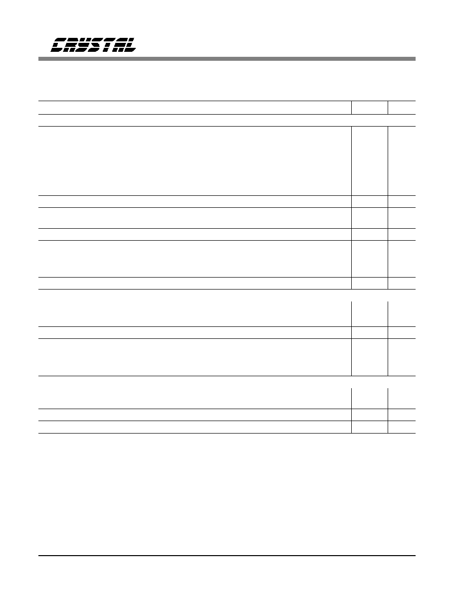
sckh
sckl
sckw
t
t
t
MSB
MSB-1
*SCLK shown for DSCK = 0, SCLK inverted for DSCK = 1.
tdpd
SDOUT
LRCK
SCLK*
SDIN
dh
t
ds
t
lrpd
t
lrcks
t
lrckd
t
Serial Audio Port Data I/O timing
CS4222
4
DS236PP3
SWITCHING CHARACTERISTICS - CONTROL PORT
(T
A
= 25
∞
C VD, VA = 5V
±
5%; Inputs: logic 0 = DGND, logic 1 = VD, C
L
= 30pF)
Parameter
Symbol
Min
Max
Units
SPI Mode (SPI/I
2
C = 0)
CCLK Clock Frequency
f
sck
-
6
MHz
RST rising edge to CS falling
t
srs
500
-
ns
CCLK edge to CS falling
(Note 9)
t
spi
500
-
ns
CS High Time Between Transmissions
t
csh
1.0
-
µ
s
CS Falling to CCLK Edge
t
css
20
-
ns
CCLK Low Time
t
scl
66
-
ns
CCLK High Time
t
sch
66
-
ns
CDIN to CCLK Rising Setup Time
t
dsu
40
-
ns
CCLK Rising to DATA Hold Time
(Note 10)
t
dh
15
-
ns
Rise Time of CCLK and CDIN
(Note 11)
t
r2
-
100
ns
Fall Time of CCLK and CDIN
(Note 11)
t
f2
-
100
ns
Notes:
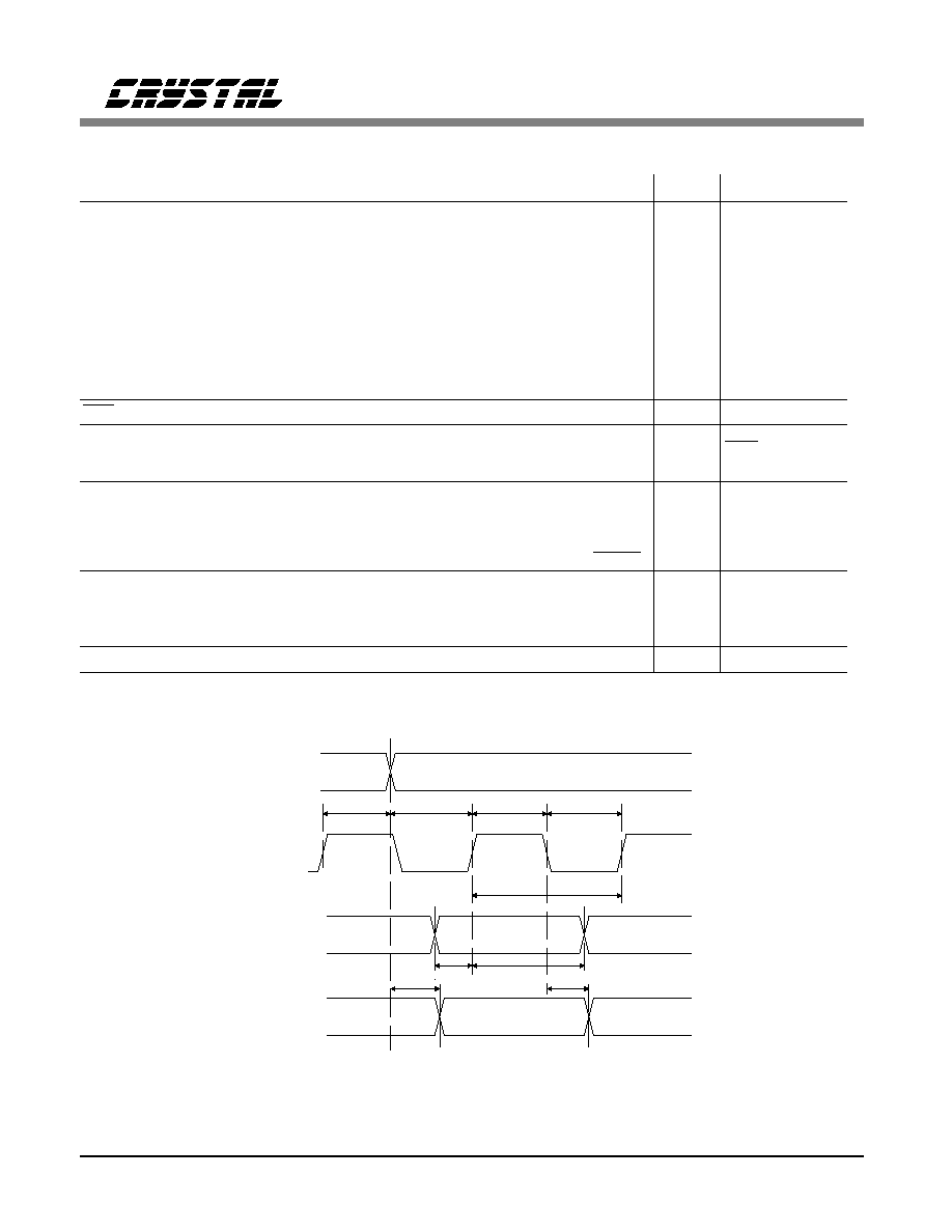
9. t
spi
only needed before first falling edge of CS after RST rising edge.
t
spi
= 0 at all other times.
10. Data must be held for sufficient time to bridge the transition time of CCLK.
11. For F
SCK
< 1 MHz
t r2
t f2
t dsu t dh
t sch
t scl
CS
CCLK
CDIN
t css
t csh
t spi
t srs
RST
CS4222
DS236PP3
5
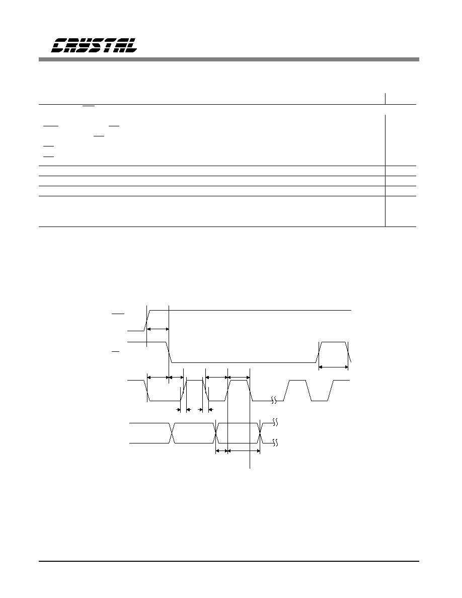
t
buf
t
hdst
t
hdst
t
low
t r
t f
t
hdd
t
high
t sud
t sust
t susp
Stop
Start
Start
Stop
Repeated
SDA
SCL
t
irs
RST
SWITCHING CHARACTERISTICS - CONTROL PORT
(T
A
= 25
∞
C; VD, VA = 5V
±
5%; Inputs: logic 0 = DGND, logic 1 = VD, C
L
= 30pF)
Parameter
Symbol
Min
Max
Units
I
2
C
Æ
Mode (SPI/I
2
C = 1)
(Note 12)
SCL Clock Frequency
f
scl
-
100
kHz
RST Rising Edge to Start
t
irs
500
-
ns
Bus Free Time Between Transmissions
t
buf
4.7
-
µ
s
Start Condition Hold Time (prior to first clock pulse)
t
hdst
4.0
-
µ
s
Clock Low Time
t
low
4.7
-
µ
s
Clock High Time
t
high
4.0
-
µ
s
Setup Time for Repeated Start Condition
t
sust
4.7
-
µ
s
SDA Hold Time from SCL Falling
(Note 13)
t
hdd
0
-
µ
s
SDA Setup Time to SCL Rising
t
sud
250
-
ns
Rise Time of Both SDA and SCL Lines
t
r
-
1
µ
s
Fall Time of Both SDA and SCL Lines
t
f
-
300
ns
Setup Time for Stop Condition
t
susp
4.7
µ
s
Notes: 12. Use of the I
2
C
Æ
bus interface requires a license from Philips.
I
2
C
Æ
is a registered trademark of Philips Semiconductors.
13. Data must be held for sufficient time to bridge the 300ns transition time of SCL.
CS4222
6
DS236PP3
ABSOLUTE MAXIMUM RATINGS
(AGND, DGND = 0V, all voltages with respect to 0V.)
Parameter
Symbol
Min
Typ
Max
Units
Power Supplies
Digital
VD
-0.3
-
6.0
V
Analog
VA
-0.3
-
6.0
V
Input Current
(Note 14)
-
-
±
10
mA
Analog Input Voltage
(Note 15)
-0.7
-
VA+0.7
V
Digital Input Voltage
(Note 15)
-0.7
-
VD+0.7
V
Ambient Temperature
(Power Applied)
-55
-
+125
∞C
Storage Temperature
-65
-
+150
∞C
Warning:
Operation at or beyond these limits may result in permanent damage to the device.
Normal operation is not guaranteed at these extremes.
Note: 14. Any pin except supplies. Transient currents of up to
±
100mA on the analog input pins will
not cause SCR latch-up.
15. The maximum over or under voltage is limited by the input current.
RECOMMENDED OPERATING CONDITIONS
(AGND, DGND = 0V, all voltages with respect
to 0V.)
Parameter
Symbol
Min
Typ
Max
Units
Power Supplies
Digital
VD
4.75
5.0
5.25
V
Analog
VA
4.75
5.0
5.25
V
VA - VD
-
-
0.4
V
Operating Ambient Temperature
T
A
-10
25
70
∞C
DIGITAL CHARACTERISTICS
(TA = 25 ∞C; VA, VD = 5V
±
5%)
Parameter
Symbol
Min
Typ
Max
Units
High-level Input Voltage
V
IH
2.8
-
VD+0.3
V
Low-level Input Voltage
V
IL
-0.3
-
1.0
V
High-level Output Voltage at I
0
= -2.0 mA
V
OH
VD-1.0
-
-
V
Low-level Output Voltage at I
0
= 2.0 mA
V
OL
-
-
0.4
V
Input Leakage Current
(Digital Inputs)
-
-
10
µ
A
Output Leakage Current
(High Impedance Digital Outputs)
-
-
10
µ
A
CS4222
DS236PP3
7
AINL+
AINL-
1 µF
+
0.1 µF
2
0.1 µF + 1 µF
+5V
Supply
21
6
VA
VD
Ferrite Bead
2.2 nF
150
150
AINR+
AINR-
2.2 nF
150
150
Digital
Audio
Source
20
19
17
16
18
22
7
AGND
DGND
25
26
Analog
Filter
AOUTL+
AOUTL-
24
23
Analog
Filter
AOUTR+
AOUTR-
10
11
Microcontroller
SCL/CCLK
SDA/CDIN
12
AD0/CS
8
9
Audio
DSP
SDOUT
SDIN
4
LRCK
5
SCLK
3
MCLK
R
s
R
s
CS4222
27
2
RST
SMUTE
R = 500
13
DEM0
DEM1
NC
1
NC
14
NC
15
NC
28
Note: Pins 10,11, and 12
should be tied to DGND
in stand-alone mode.
R
s
R
s
R
s
1
R = 50
s
s
1
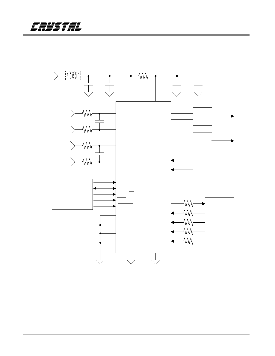
Figure 1. Recommended Connection Diagram
(Also see recommended layout diagram, Figure 10)
CS4222
8
DS236PP3
FUNCTIONAL DESCRIPTION
Overview
The CS4222 has 2 channels of 20-bit analog-to-
digital conversion and 2 channels of 20-bit
digital-to-analog conversion. All ADCs and
DACs are delta-sigma converters. The DAC out-
p ut s h ave a d ju st ab le o utp ut a tte nua tio n
implemented in 0.5 dB step resolution. The de-
vice also includes a soft mute function and
digital de-emphasis for 32, 44.1, and 48 kHz.
Digital audio data for the DACs and from the
ADCs is communicated over separate serial
ports. This allows concurrent writing to and
reading from the device. Control for the func-
tions available on the CS4222 are communicated
over a serial microcontroller interface. Figure 1
shows the recommended connection diagram for
the CS4222.
The device can be operated with or without the
control port interface. Additional functions are
available when the control port interface is used
as outlined in Table 1.
Control Port
Stand-alone
Volume control
-
Adjustable Mute ramp rate
Fixed Mute ramp rate
Enable zero crossing detect
Disabled
Disable mute on zero input
Enabled
De-emphasis
De-emphasis
Mute DAC outputs
Mute DAC outputs
ADC Input Peak Level
Detect
-
16, 18, 20 bit Interface
20 bit I
2
S Interface
Individual ADC/DAC power
down
Codec power down
Cal on command
Cal on power-up
High pass enable/disable
High pass enabled
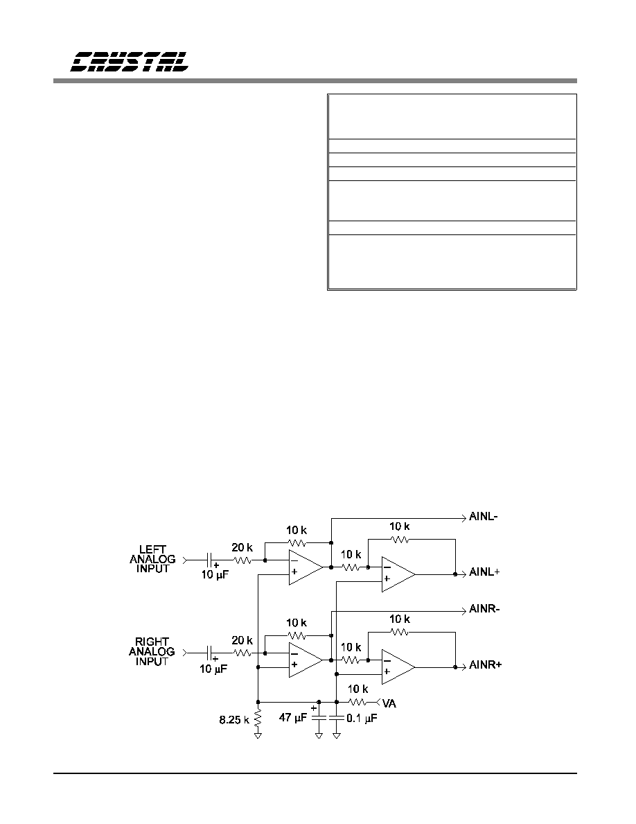
Analog Inputs
Line Level Inputs
AINR-, AINR+, AINL-, and AINL+ are the dif-
ferential line level input pins (See Figure 1).
Figure 2 shows an AC coupled optional input
buffer which combines level shifting with single-
ended to differential conversion. Analog inputs
must be DC coupled into the CS4222 with a
2.3V common mode input voltage. Any DC off-
Figure 2. Optional Line Input Buffer
Table 1. Control Port vs. Stand-alone
CS4222
DS236PP3
9
set at the input to the CS4222 will be removed
by the internal high-pass filters. See Figure 3 for
the differential input signal description. The
ADC outputs may be muted (set to zero) by
writing the ADMR and ADML bits, and the
ADC can be independently powered down using
the PDAD bit. ADMR, ADML, and PDAD are
all located in the ADC control byte (#1).
Input Level Monitoring
The CS4222 includes independent Peak Input
Level Monitoring for each channel. The analog-
to-digital converter continually monitors the peak
digital signal for both channels, prior to the digi-
tal limiter, and records these values in the
LVL2-0 (left channel) and LVR2-0 (right chan-
nel) bits in the Converter Status Report Byte
(#6). These bits indicate whether the input level
is clipping, -1 to -6 dB from full scale in 1 dB
resolution, or below -6 dB from full scale. The
LVL/LVR bits are "sticky" bits and are reset to
zero when read.
High Pass Filter
The operational amplifiers in the input circuitry
driving the CS4222 may generate a small DC
offset into the A/D converter. The CS4222 in-
cludes a high pass filter after the decimator to
remove any DC offset which could result in re-
cording a DC level, possibly yielding "clicks"
when switching between devices in a multichan-
nel system. The characteristics of this first-order
high pass filter are outlined below for Fs equal
to 48 kHz. The filter response scales linearly
with sample rate. The high pass filter may be de-
feated independently for the left and right
channels by writing HPDR and HPDL in the
ADC control byte (#1).
Frequency Response
-3dB @ 3.7 Hz
-0.1 dB @ 20 Hz
Phase Deviation
10 degrees @ 20 Hz
Passband Ripple
None
Table 2. High Pass Filter Characteristics
Analog Outputs
Line Level Outputs
The CS4222 contains an on-chip buffer amplifier
producing differential outputs capable of driving
10 k
loads. Each output (AOUTL+, AOUTL-,
AOUTR+, AOUTR-) will produce a nominal
2.83 Vpp (1 Vrms) output with a 2.3 volt com-
mon mode for a full scale digital input. This is
equivalent to a 5.66 Vpp (2 Vrms) differential
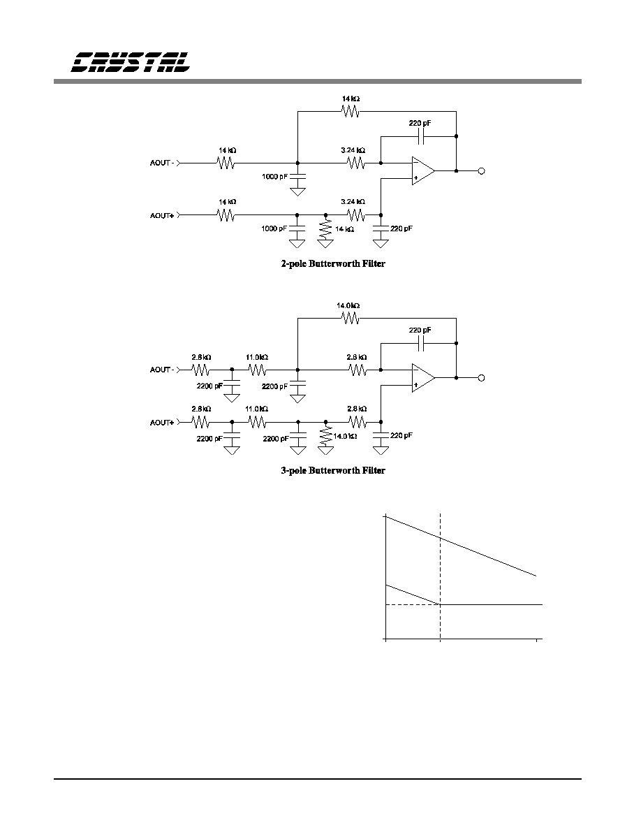
signal as shown in Figure 3. The recommended
off-chip analog filter is either a 2nd order Butter-
worth or a 3rd order Butterworth, if greater
out-of-band noise filtering is desired. The
CS4222 DAC interpolation filter has been pre-
c o m pe n s at e d fo r a n ext e rn al 2 n d or der
Butterworth filter with a 3dB corner at Fs, or a
3rd order Butterworth filter with a 3dB corner at
0.75 Fs to provide a flat frequency response and
linear phase over the passband (see Figure 4 for
Fs = 48 kHz). If the recommended filter is not
used, small frequency response magnitude and
phase errors will occur. In addition to providing
out-of-band noise attenuation, the output filters
shown in Figure 4 provide differential to single-
ended conversion.
The DACs can be powered down using the
PDDA bit in the DAC control register (#2).
CS4222
AIN+/AOUT+
AIN+/AOUT-
Full Scale Output level = (AOUT+) - (AOUT-)= 5.66 Vpp
(2.3 + 1.4)V
2.3V
(2.3 - 1.4)V
(2.3 + 1.4)V
2.3V
(2.3 - 1.4)V
Full Scale Input level = (AIN+) - (AIN-)= 5.66 Vpp
Figure 3. Full Scale Input/Output Voltage
CS4222
10
DS236PP3
Analog/Digital Volume Control - Control Port
Mode Only
The DAC outputs are each routed through an at-
tenuator which is adjustable in 0.5 dB steps.
Output attenuation is available through the Out-
put Attenuator Data Bytes (#3 & #4). Level
changes are implemented with an analog volume
control until the residual output noise is equal to
the noise floor in the mute state at which point
volume changes are performed digitally. This
technique is superior to purely digital volume
control techniques as the noise is attenuated by
the same amount as the signal, thus preserving
dynamic range (see Figure 5).
The CS4222 implements a "soft" volume control
whereby level changes are achieved by ramping
from the current level to the new level in 0.5 dB
steps. The default rate of volume change is 8
LRCK cycles for each 0.5 dB step (equivalent to
647
µ
s at Fs = 48 kHz). The rate of volume
Figure 4.
Signal
Noise
0
0
-113.5
Attenuation (dB)
Am
p
l
i
t
u
d
e
(
d
B)
Analog Digital
Figure 5. Hybrid Analog/Digital Attenuation
CS4222
DS236PP3
11
change is adjustable to 4, 16, or 32 LRCK cycles
with the RMP1/0 bits in the DAC control byte
(#2).
"Soft" volume control may be disabled through
the SOFT bit in the DAC bit Control Byte (#2).
When "soft" volume control is defeated, level
changes step from the current level to the new
level in a single step. The volume change takes
effect on a zero crossing to minimize audible ar-
tifacts. If there is no zero crossing, then the
requested level change will occur after a time-
out period between 512 and 1024 sample periods
(10.7 ms to 21.3 ms at 48 kHz sample rate).
There is a separate zero crossing detector for
each channel. ACCR and ACCL bits in the Con-
verter Status Report Byte (#6) give feedback on
when a volume control change has taken effect
for the right and left channel. This bit goes high
when a new setting is loaded and returns low
when it has taken effect.
Soft Mute/Mute on Zero Input Data
Muting can be achieved via hardware or soft-
ware control. Soft mute can be achieved by
lowering the SMUTE pin at which point the out-
put level will ramp down in 0.5 dB steps to a
muted state. Upon returning the SMUTE pin
high, the output will ramp up to the volume con-
trol setting in the Output Attenuator Data Bytes
(#3 & #4). "Soft" mute may be disabled through
the SOFT bit in the DAC Control Byte (#2).
When "soft" mute is defeated, muting occurs on
zero crossings or after a time-out period, similar
to the volume control changes.
Under software control, each output can be inde-
pendently muted via mute control bits, MUTR
and MUTL, in the DAC Control Byte (#2). Soft
mute or zero crossing mute will be implemented
depending on the state of the SOFT bit in the
DAC Control Byte (#2).
Muting on consecutive zero input data is also
provided where all DAC outputs will mute if
they receive between 512 and 1024 consecutive
zeros (or -1 code). Detection and muting is done
independently for left and right channels. A sin-
gle non-zero value will immediately unmute the
DAC output. This feature is enabled on power-
up, and it may be disabled with the MUTC bit in
the DAC Control Byte (#2).
Master Clock Generation
The Master Clock, MCLK, is used to operate the
digital filters and the delta-sigma modulator.
MCLK must be either 256
x
, 384
x
, or 512
x
the
desired Input Sample Rate, Fs. Fs is the fre-
quency at which digital audio samples for each
channel are input to the DAC or output from the
ADC and is equal to the LRCK frequency. The
MCLK to LRCK frequency ratio is detected
automatically during the initialization sequence by
counting the number of MCLK transitions during
a single LRCK period. Internal dividers are then
set to generate the proper clocks for the digital
filters, delta-sigma modulators and switched-ca-
pacitor filter. Table 3 illustrates the standard
audio sample rates and the required MCLK fre-
quencies. If MCLK stops for 10
µ
s, the CS4222
will enter a power down state until the clock re-
turns. The control port registers will maintain
their current settings. It is required to have
SCLK and LRCK derived from the master
clock.
Fs (kHz)
MCLK (MHz)
256x
384x
512x
32
8.1920
12.2880
16.3840
44.1
11.2896
16.9344
22.5792
48
12.2880
18.4320
24.5760
Table 3. Common Clock Frequencies
CS4222
12
DS236PP3
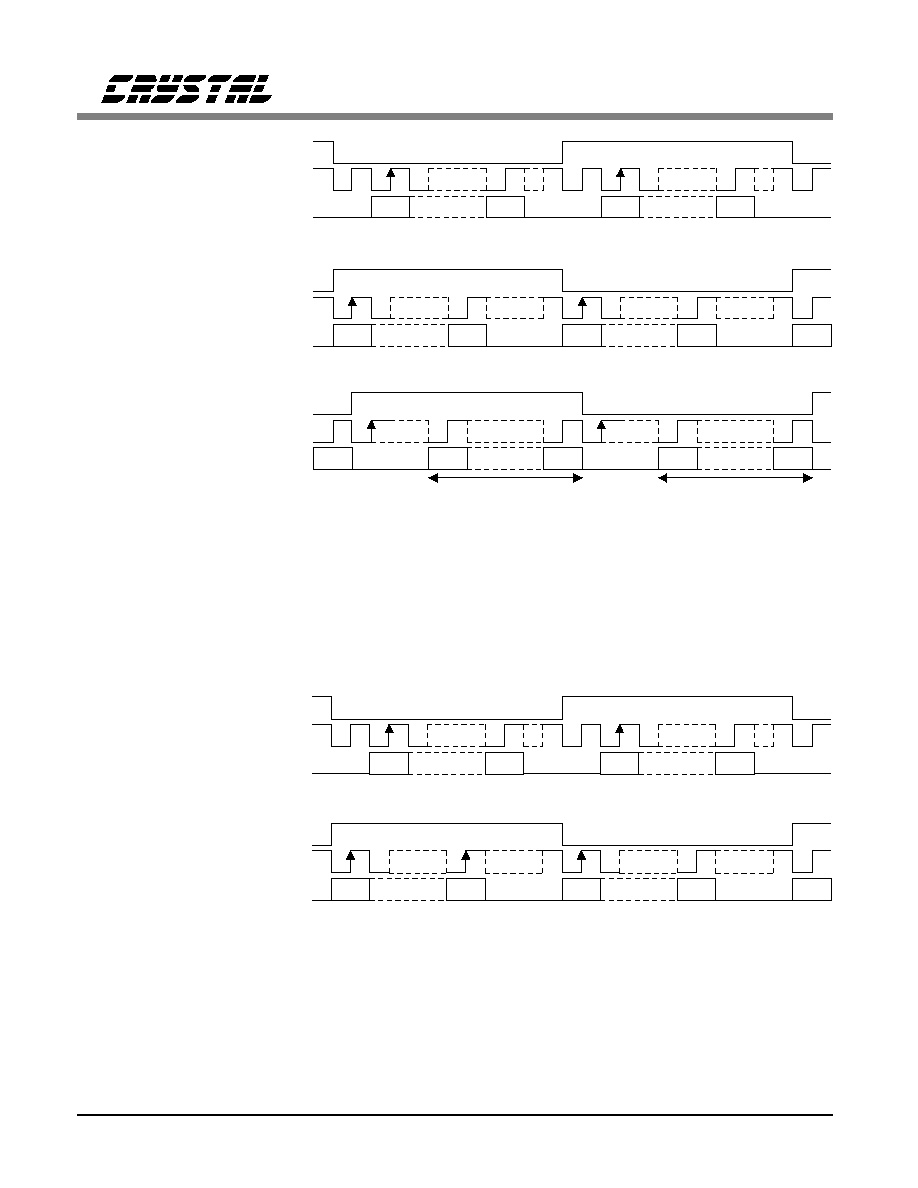
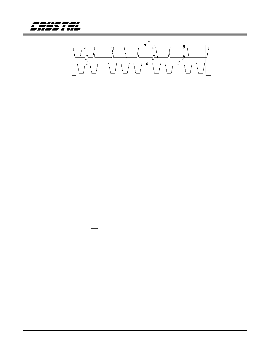
LRCK
FORMAT 1:
SCLK
SDIN
MSB
LSB
Left
Right
MSB
LSB
MSB
LRCK
FORMAT 0:
SCLK
SDIN
MSB
LSB
Left
Right
MSB
LSB
Note: SCLK shown for DSCK = 0. SCLK inverted for DSCK = 1.
(Stand-Alone and
Control Port Mode)
(Control Port
Mode only)
Figure 7. Audio DSP Port Data Output Formats.
LRCK
FORMAT 2, 3, 4:
SCLK
SDIN
Format 2: M = 20
Format 3: M = 18
Format 4: M = 16
LSB
LSB
MSB
LSB
MSB
Left
Right
M SCLKs
M SCLKs
LRCK
FORMAT 1:
SCLK
SDIN
MSB
LSB
Left
Right
MSB
LSB
MSB
LRCK
FORMAT 0:
SCLK
SDIN
MSB
LSB
Left
Right
MSB
LSB
Note: SCLK shown for DSCK = 0. SCLK inverted for DSCK = 1.
(Stand-Alone and
Control Port Mode)
(Control Port
Mode only)
(Control Port
Mode only)
Figure 6. Audio DSP Data Input Formats.
CS4222
DS236PP3
13
Serial Audio Data Interface
Serial Audio Interface Signals
The serial interface clock, SCLK, is used for
transmitting and receiving audio data. The active
edge of SCLK is chosen by setting the DSCK bit
in the DSP Port Mode Byte (#6); the default
upon power-up is that data is valid on the rising
edge for both input and output. SCLK is an in-
put from an external source and at least 20
SCLK's per half period of LRCK are required
for proper operation.
The Left/Right clock (LRCK) is used to indicate
left and right data and the start of a new sample
period. The frequency of LRCK must be equal
to the system sample rate, Fs.
SDIN is the data input pin which drives a pair of
DACs. SDOUT is the output data pin from the
ADC's.
Serial Audio Interface Formats
The serial audio port supports 5 input and 2 out-
put formats, shown in Figures 6 and 7. These
formats are chosen through the DSP Port Mode
Byte (#5) with the DDO and DDI2/1/0 bits. The
data output format is 20 bits and may be left jus-
tified or I
2
S compatible depending on the state
of the DDO bit. The input data format is set
with the DDI bits to be left or right justified or
I
2
S compatible. In addition, the polarity of the
SCLK edge used to clock in/out data from the
CS4222 may be set via the DSCK bit in the DSP
Port Mode Byte (#5). The default input and out-
put format is I
2
S compatible.
Control Port Interface
The control port is used to load all the internal
settings. The operation of the control port may
be completely asynchronous with the audio sam-
ple rate. However, to avoid potential interference
problems, the control port pins should remain
static if no operation is required.
The control port has 2 modes: SPI and I
2
C
Æ
,
with the CS4222 operating as a slave device. If
I
2
C operation is desired, AD0/CS should be tied
to VD or DGND. If the CS4222 ever detects a
negative transition on AD0/CS after power-up,
SPI mode will be selected.
SPI Mode
In SPI mode, CS is the CS4222 chip select sig-
nal, CCLK is the control port bit clock, CDIN is
the input data line from the microcontroller and
the chip address is 0010000. All signals are in-
puts and data is clocked in on the rising edge of
CCLK.
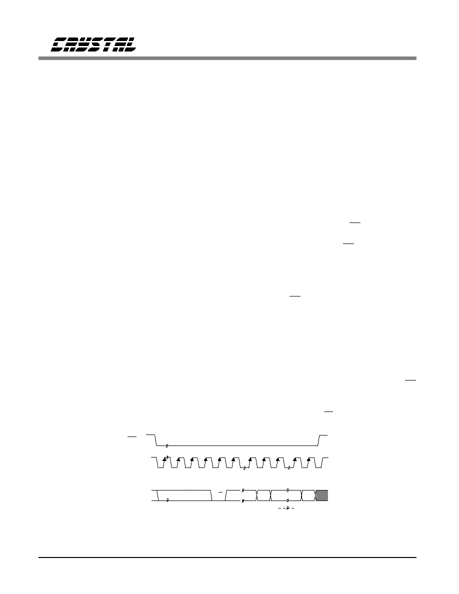
Figure 8 shows the operation of the control port
in SPI mode. To write to a register, bring CS
low. The first 7 bits on CDIN form the chip ad-
dress, and must be 0010000. The eighth bit is a
read/write indicator (R/W), which must be low
to write. Register reading from the CS4222 is
MAP
MSB
LSB
DATA
byte 1
byte n
R/W
MAP = Memory Address Pointer
ADDRESS
CHIP
CDIN
CCLK
CS
0010000
Figure 8. Control Port Timing, SPI mode
CS4222
14
DS236PP3
not supported in the SPI mode. The next 8 bits
form the Memory Address Pointer (MAP), which
is set to the address of the register that is to be
updated. The next 8 bits are the data which will
be placed into register designated by the MAP.
The CS4222 has a MAP auto increment capabil-
ity, enabled by the INCR bit in the MAP register.
If INCR is a zero, then the MAP will stay con-
stant for successive writes. If INCR is set to a 1,
then MAP will auto increment after each byte is
written, allowing block writes of successive reg-
isters. Register reading from the CS4222 is not
supported in the SPI mode.
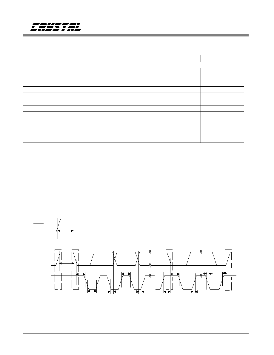
I
2
C
Æ
Mode
In I
2
C
Æ
mode, SDA is a bidirectional data line.
Data is clocked into and out of the part by the
clock, SCL, with the clock to data relationship as
shown in Figure 9. There is no CS pin. Pin AD0
forms the partial chip address and should be tied
to VD or DGND as desired. The upper 6 bits of
the 7 bit address field must be 001000. To com-
municate with the CS4222 the LSB of the chip
address field, which is the first byte sent to the
CS4222, should match the setting of the AD0
pin. The eighth bit of the address byte is the
R/W bit (high for a read, low for a write). If the
operation is a write, the next byte is the Memory
Address Pointer which selects the register to be
read or written. If the operation is a read, the
contents of the register pointed to by the Mem-
ory Address Pointer will be output. Setting the
auto increment bit in MAP, allows successive
reads or writes of consecutive registers. Each
byte is separated by an acknowledge bit. Use of
the I
2
C bus
Æ
compatible interface requires a li-
cense from Philips. I
2
C bus
Æ
is a registered
trademark of Philips Semiconductor.
Control Port Bit Definitions
All registers can be written and read in I
2
C
mode, except the Converter Status Report Byte
(#6) and the CLKE and CALP bits in the ADC
control byte (#1) which are read only. SPI mode
only allows for register writing. See the follow-
ing bit definition tables for bit assignment
information.
SDA
SCL
001000
ADDR
AD0
R/W
Start
ACK
DATA
1-8
ACK
DATA
1-8
ACK
Stop
Note: If operation is a write, this byte contains the Memory Address Pointer, MAP.
Note 1
Figure 9. Control Port Timing, I
2
C
Æ
Mode
CS4222
DS236PP3
15

De-Emphasis
The CS4222 is capable of digital de-emphasis
for 32, 44.1, or 48 kHz sample rates. Imple-
mentation of digital de-emphasis requires
reconfiguration of the digital filter to maintain
the filter response shown in Figure 10 at multi-
ple sample rates.
De-emphasis control is achieved with the
DEM1/0 pins or through the DEM2-0 bits in the
DAC Control Byte (#2). The default state on
power-up is de-emphasis controlled via the
DEM1/0 pins (DEM2-0 bits=0). DEM1/0 pin
control is defined in Table 4.
DEM 1
DEM 0
De-emphasis
0
0
32 kHz
0
1
44.1 kHz
1
0
48 kHz
1
1
OFF
Table 4. De-Emphasis filter control
Power-up/Reset/Power Down/Calibration
Upon power up, the user should hold RST=0 for
approximately 10 ms. In this state, the control
port is reset to its default settings and the part
remains in the power down mode. At the end of
RST, the device performs an offset calibration
which lasts approximately 50 ms after which the
device enters normal operation. A calibration
may also be initiated via the CAL bit in the
ADC Control Byte (#1). The CALP bit in the
ADC Control Byte is a read only bit indicating
the status of the calibration.
Reset/Power Down is achieved by lowering the
RST pin causing the part to enter power down.
Once RST goes high, the control port is func-
tional and the desired settings should be loaded.
The CS4222 will also enter power down mode if
the master clock source stops for approximately
10
µ
s or if the LRCK is not synchronous to the
master clock. The control port will retain its
current settings.
Additionally, the PDAD (ADC Control Byte #1)
and PDDA (DAC Control Byte #2) bits can be
used to power down the ADC's and DAC's inde-
pendently. If both are set to 1, the CS4222 will
power down the entire chip. The control port
will retain its current settings.
The CS4222 will mute the analog outputs and
enter the power down mode if the supply drops
below approximately 4 volts.
Power Supply, Layout and Grounding
The CS4222 should be located on the analog
ground plane along with associated analog cir-
cuitry and should be positioned near the split
between ground planes (see Figure 11). Prefer-
ably, the device should also have its own power
plane. The +5V supply should be connected to
the CS4222 via a ferrite bead, positioned closer
than 1" to the device. A single connection be-
Gain
dB
-10dB
0dB
Frequency
T2 = 15
µ
s
T1=50
µ
s
F1
F2
Figure 10. De-emphasis Curve.
CS4222
16
DS236PP3
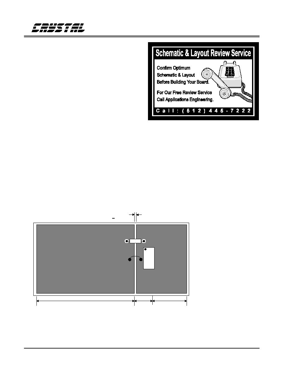
tween the CS4222 ground and the board ground
should be positioned as shown in Figure 11. See
the CDB4222 evaluation board data sheet for
recommended layout of the decoupling compo-
nents.
ADC and DAC Filter Response Plots
Figures 12 through 17 show the overall fre-
quency response, passband ripple and transition
band for the CS4222 ADC's and DAC's.
Digital
Ground
Plane
Note that the CS4222
is oriented with its
digital pins towards the
digital end of the board.
CPU & Digital
Logic
Codec
digital
signals
Analog
Ground
Plane
1/8"
>
CS
42
22
+5V
Ferrite
Bead
Ground
Connection
Codec
analog
signals &
components
Figure 11. Suggested Layout Guideline (See CDB4222 Data Sheet)
CS4222
DS236PP3
17
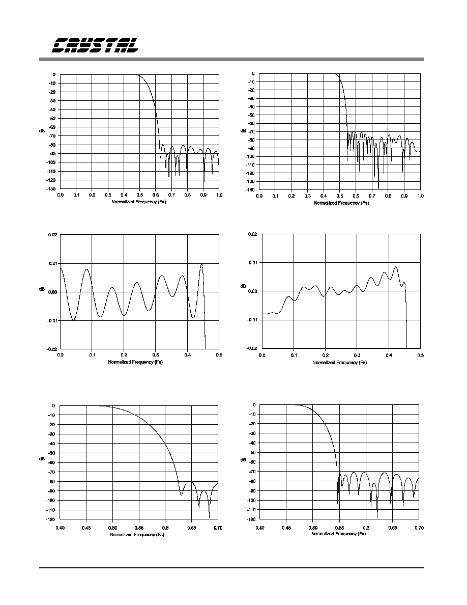
Figure 12. ADC Filter Response.
Figure 13. ADC Passband Ripple.
Figure 14. ADC Transition Band.
Figure 15. DAC Frequency Response.
Figure 16. DAC Passband Ripple.
Figure 17. DAC Transition Band.
CS4222
18
DS236PP3

Memory Address Pointer (MAP)
B7
B6
B5
B4
B3
B2
B1
B0
INCR
0
0
0
0
MAP2 MAP1 MAP0
MAP2-MAP0
Register Pointer
INCR
Auto Increment Control Bit
0 - No auto increment
1 - Auto increment on
This register defaults to 00h.
Reserved Byte (0)
This byte is reserved for internal use and must
be set to 00h for normal operation.
This register defaults to 00h.
ADC Control Byte (1)
B7
B6
B5
B4
B3
B2
B1
B0
PDAD HPDR HPDL ADMR ADML
CAL CALP CLKE
PDAD
Power Down ADC
0 - Normal
1 - Power down
HPDR-HPDL
High pass filter defeat, right and left
0 - High pass filters active
1 - High pass filters defeated
ADMR-ADML ADC Muting, right and left
0 - Normal
1 - Output muted
CAL
Calibration control bit
0 - Normal operation
1 - Rising edge initiates calibration
The following bits are read only:
CALP
Calibration status
0 - Calibration done
1 - Calibration in progress
CLKE
Clocking Error
0 - No error
1 - error
This register defaults to 00h.
DAC Control Byte (2)
B7
B6
B5
B4
B3
B2
B1
B0
PDDA MUTC MUTR MUTL SOFT
0
RMP1
RMP0
PDDA
Power Down DAC
0 - Normal
1 - Power down
MUTC
Controls mute on consecutive zeros
function
0 - 512 consecutive zeros will mute DAC
1 - DAC output will not mute on zeros.
MUTR-MUTL Mute control bits
0 - Normal output level
1 - Selected DAC output muted
SOFT
Soft Mute Control
0 - Volume control changes, muting and
mute-on-zeros occur with "ramp"
1 - Volume control changes, muting and
mute-on-zeros occur on zero crossings
RMP1-0
Soft Volume 0.5 dB step rate
0 - 1 step per 8 LRCK's
1 - 1 step per 4 LRCK's
2 - 1 step per 16 LRCK's
3 - 1 step per 32 LRCK's
This register defaults to 00h.
CS4222
DS236PP3
19

Output Attenuator Data Byte (3, 4)
B7
B6
B5
B4
B3
B2
B1
B0
ATT7
ATT6
ATT5
ATT4
ATT3
ATT2
ATT1
ATT0
ATT7-ATT0
Sets attenuator level
0 - No attenuation
227 - 113.5 dB attenuation
>227 - DAC muted
ATT0 represents 0.5 dB of attenuation
This register defaults to 00h.
DSP Port Mode Byte (5)
B7
B6
B5
B4
B3
B2
B1
B0
DEM2 DEM1 DEM0 DSCK DDO DDF2 DDF1 DDF0
DEM2-0
Selects de-emphasis control source
0 - De-emphasis controlled by pins
1 - 44.1 kHz de-emphasis setting
2 - 48 kHz de-emphasis setting
3 - 32 kHz de-emphasis setting
4 - De-emphasis disabled
5 - Not used
6 - Not used
7 - Not used
DSCK
Set the polarity of clocking data
0 - Data valid on rising edge of SCLK
1 - Data valid on falling edge of SCLK
DDO
Data output format
0 - I
2
S compatible
1 - Left justified
DDI2-DDI0
Data input format
0 - I
2
S compatible
1 - Left justified
2 - Right justified, 20-bit
3 - Right justified, 18-bit
4 - Right justified, 16-bit
5 - Not used
6 - Not used
7 - Not used
This register defaults to 00h.
Converter Status Report Byte (Read Only) (6)
B7
B6
B5
B4
B3
B2
B1
B0
ACCR ACCL LVR2
LVR1
LVR0
LVL2
LVL2
LVL0
ACCR-ACCL
Acceptance bit
0 - ATT7-0 has been accepted
1 - New setting waiting for zero crossing
LVL2-0,LVR2-0 Left and Right ADC output level
0 - Normal output levels
1 - -6 dB level
2 - -5 dB level
3 - -4 dB level
4 - -3 dB level
5 - -2 dB level
6 - -1 dB level
7 - Clipping
LVL2-0 and LVR2-0 bits are 'sticky'. They constantly
monitor the ADC output for the peak levels and hold
the maximum output. They are reset to 0 when read.
This register is read only.
CS4222
20
DS236PP3
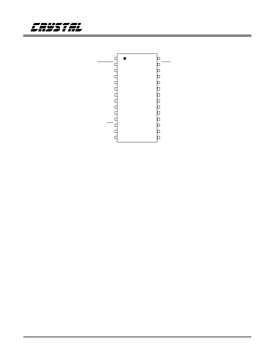
PIN DESCRIPTIONS
Power Supply
VA - Positive Analog Power, Pin 21.
Positive analog supply. Nominally +5 volts.
VD - Positive Digital Power, Pin 6.
Positive supply for the digital section. Nominally +5 volts.
AGND - Analog Ground, Pin 22.
Analog ground reference.
DGND - Digital Ground, Pin 7.
Digital ground for the digital section.
Analog Inputs
AINR-, AINR+ - Differential Right Channel Analog Input, Pins 16 and 17.
Analog input connections of the right channel differential inputs. Typically 2 Vrms differential
(1 Vrms for each input pin) for a full-scale analog input signal.
AINL-, AINL+ - Differential Left Channel Analog Input, Pins 19 and 20.
Analog input connections of the left channel differential inputs. Typically 2 Vrms differential
(1 Vrms for each input pin) for a full-scale analog input signal.
NC
NC
SMUTE
RST
MCLK
AOUTL-
LRCK
AOUTL+
SCLK
AOUTR+
VD
AOUTR-
DGND
AGND
SDOUT
VA
SDIN
AINL+
SCL/CCLK
AINL-
SDA/CDIN
DEM1
AD0/CS
AINR+
DEM0
AINR-
NC
NC
1
2
3
4
5
6
7
8
9
10
11
12
13
14
28
27
26
25
24
23
22
21
20
19
18
17
16
15
CS4222
DS236PP3
21

Analog Outputs
AOUTR-, AOUTR+ - Differential Right Channel Analog Outputs, Pins 23 and 24.
Analog output connections for the Right channel differential outputs. Nominally 2 Vrms
(differential) for full-scale digital input signal.
AOUTL-, AOUTL+ - Differential Left Channel Analog Outputs, Pins 25 and 26.
Analog output connections for the Left channel differential outputs. Nominally 2 Vrms
(differential) for full-scale digital input signal.
Digital Inputs
MCLK - Master Clock, Pin 3.
Clock source for the delta-sigma modulator sampling and digital filters. The frequency of this
clock must be either 256x, 384x, or 512x Fs.
LRCK - Left/Right Clock, Pin 4.
LRCK determines which channel, left or right, is to be input/output on SDIN/SDOUT.
Although the outputs for each ADC channel are transmitted at different times, Left/Right pairs
represent simultaneously sampled analog inputs. LRCK is an input clock whose frequency
must be equal to Fs.
SCLK - Serial Data Clock, Pin 5.
Clocks the individual bits of the serial data out from SDOUT and in from SDIN.
SDIN - Serial Data Input, Pin 9.
Two's complement MSB-first serial data of either 16, 18, or 20 bits is input on this pin. The
data is clocked into the CS4222 via the SCLK clock and the channel is determined by the
LRCK clock. The default interface format on power-up is an I
2
S compatible 20-bit interface.
This may be changed by writing the control port (DSP Port Mode Byte #5).
DEM1, DEM0 - De-Emphasis Select, Pins 18 and 13.
Controls the activation of the standard 50/15
µ
s de-emphasis filter. 32, 44.1, or 48 kHz sample
rate selection defined in Table 4.
SMUTE - Soft Mute, Pin 2.
SMUTE low activates a muting function for both the left and right channel D/A converter
outputs. Soft muting is achieved by ramping down the volume in 0.5 dB steps until achieving
mute if SOFT bit (DAC Control Byte #2) is set to 0 (default).
Digital Outputs
SDOUT - Serial Data Output, Pin 8.
Two's complement MSB-first serial data of 20 bits is output on this pin. The data is clocked
out via the SCLK clock and the channel is determined by LRCK.
CS4222
22
DS236PP3

Control Port Signals
SCL/CCLK - Serial Control Interface Clock, Pin 10.
SCL/CCLK is the serial control interface clock and is used to clock control bits into and out of
the CS4222 This pin should be tied to DGND in stand-alone mode.
AD0/CS - Address Bit/Control Port Chip Select, Pin 12.
In I
2
CÆ mode, AD0 is a chip address bit. In SPI mode, CS is used to enable the control port
interface on the CS4222. The CS4222 will enter SPI mode if a negative transition is ever seen
on this pin after power up. This pin should be tied to DGND in stand-alone mode.
SDA/CDIN - Serial Control Data In, Pin 11.
SDA/CDIN is the input data line for the control port interface. This pin should be tied to
DGND in stand-alone mode.
Miscellaneous Pins
RST - Reset, Pin 27.
When low, the CS4222 enters a low power mode and all internal states are reset, including the
control port. When high, the control port becomes operational and normal operation will occur.
NC - No Connect, Pins 1, 14, 15 and 28
These pins are not connected internally and should be tied to DGND to minimize noise
coupling.
PARAMETER DEFINITIONS
Dynamic Range
The ratio of the full scale rms value of the signal to the rms sum of all other spectral
components over the specified bandwidth. Dynamic range is a signal-to-noise measurement
over the specified bandwidth made with a -60dBFS signal. 60dB is then added to the resulting
measurement to refer the measurement to full scale. This technique ensures that the distortion
components are below the noise level and do not affect the measurement. This measurement
technique has been accepted by the Audio Engineering Society, AES17-1991, and the Electronic
Industries Association of Japan, EIAJ CP-307.
Total Harmonic Distortion + Noise
The ratio of the rms value of the signal to the rms sum of all other spectral components over
the specified bandwidth (typically 20Hz to 20kHz), including distortion components. Expressed
in decibels. ADCs are measured at -1 dBFS as suggested in AES17-1991 Annex A and DACs
are measured at 0 dBFS.
CS4222
DS236PP3
23

Idle Channel Noise / Signal-to-Noise-Ratio
The ratio of the rms analog output level with 1kHz full scale digital input to the rms analog
output level with all zeros into the digital input. Measured A-weighted over a 10Hz to 20kHz
bandwidth. Units in decibels. This specification has been standardized by the Audio
Engineering Society, AES17-1991, and referred to as Idle Channel Noise. This specification has
also been standardized by the Electronic Industries Association of Japan, EIAJ CP-307, and
referred to as Signal-to-Noise-Ratio.
Total Harmonic Distortion (THD)
THD is the ratio of the test signal amplitude to the rms sum of all the in-band harmonics of the
test signal. Units in decibels.
Interchannel Isolation
A measure of crosstalk between channels. Measured for each channel at the converter's output
with no signal to the input under test and a full-scale signal applied to the other channel. Units
in decibels.
Frequency Response
A measure of the amplitude response variation from 20Hz to 20kHz relative to the amplitude
response at 1kHz. Units in decibels.
Interchannel Gain Mismatch
For the ADCs, the difference in input voltage that generates the full scale code for each
channel. For the DACs, the difference in output voltages for each channel with a full scale
digital input. Units are in decibels.
Gain Error
The deviation from the nominal full scale output for a full scale input.
Gain Drift
The change in gain value with temperature. Units in ppm/∞C.
Offset Error
For the ADCs, the deviation in LSB's of the output from mid-scale with the selected inputs tied
to a common potential. For the DAC's, the differential output voltage with mid-scale input
code. Units are in volts.
CS4222
24
DS236PP3
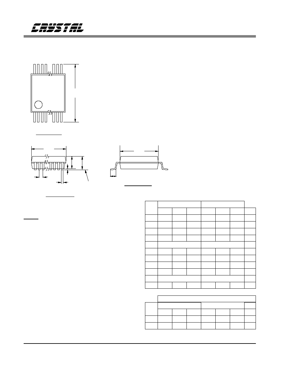
PACKAGE DIMENSIONS
E
A
A
D
E
A
1
1
SIDE VIEW
END VIEW
TOP VIEW
Seating
Plane
Notes:
1. "D" and "E " are reference datums
and do not include mold flash or
protrusions, but do include mold
mismatch and are measured at the
parting line, mold flash or protrusions
shall not exceed 0.20mm per side.
2. Dimension b does not include
dambar protrusion/intrusion.
Allowable dambar protrusion shall
be 0.13mm total in excess of b
dimension at maximum material
condition. Dambar intrusion shall
not reduce dimension b by more than
0.07mm at least material condition.
3. These dimensions apply to the flat
section of the lead between 0.10 and
0.25mm from lead tips.
N
1
3
2
SSOP Package
Dimensions
N
MILLIMETERS
MIN
NOM
MAX
20
28
6.90
7.20
7.50
9.90
10.20 10.50
Note
1
1
1
2
1
DIM
MILLIMETERS
MIN
NOM
MAX
A
A
A
b
D
E
e
E
L
N
-
-
2.13
0.05
0.15
0.25
1.62
1.75
1.88
0.22
0.30
0.38
see other table
5.00
5.30
5.60
7.40
7.80
8.20
0.63
0.90
1.03
see other table
0∞
4∞
8∞
Note
2, 3
1
1
1
2
1
e
b
2
0.61
0.65
0.69
L
INCHES
MIN
NOM
MAX
-
-
0.084
0.002
0.006 0.010
0.064
0.070 0.074
0.009
0.012 0.015
see other table
0.197
0.209 0.220
0.291
0.307 0.323
0.025
0.035 0.040
see other table
0∞
4∞
8∞
0.024
0.026 0.027
D
INCHES
MIN
NOM
MAX
0.272 0.283
0.295
0.390 0.402
0.413
1
CS4222
DS236PP3
25
