Preliminary Product Information
This document contains information for a new product.
Cirrus Logic reserves the right to modify this product without notice.
Copyright
�
Cirrus Logic, Inc. 2005
(All Rights Reserved)
Cirrus Logic, Inc.
http://www.cirrus.com
CS42518
110 dB, 192 kHz 8-Ch Codec with S/PDIF Receiver
Features
Eight 24-bit D/A, two 24-bit A/D Converters
11
0
dB DAC / 114 dB ADC Dynamic Range
-100 dB THD+N
System Sampling Rates up to 192 kHz
S/PDIF Receiver Compatible with EIAJ CP1201
and IEC-60958
Recovered S/PDIF Clock or System Clock
Selection
8:2 S/PDIF Input MUX
ADC High-pass Filter for DC Offset Calibration
Expandable ADC Channels and One-line Mode
Support
Digital Output Volume Control with Soft Ramp
Digital +/-15dB Input Gain Adjust for ADC
Differential Analog Architecture
Supports logic levels between 5 V and 1.8 V.
General Description
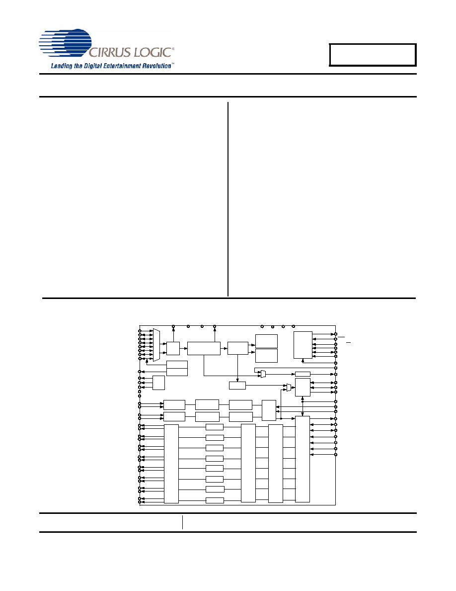
The CS42518 codec provides two analog-to-digital and eight
digital-to-analog delta-sigma converters, as well as an integrat-
ed S/PDIF receiver, in a 64-pin LQFP package.
The CS42518 integrated S/PDIF receiver supports up to eight
inputs, clock recovery circuitry and format auto-detection. The
internal stereo ADC is capable of independent channel gain
control for single-ended or differential analog inputs. All eight
channels of DAC provide digital volume control and differential
analog outputs. The general purpose outputs may be driven
high or low, or mapped to a variety of DAC mute controls or
ADC overflow indicators.
The CS42518 is ideal for audio systems requiring wide dynam-
ic range, negligible distortion and low noise, such as A/V
receivers, DVD receivers, digital speaker and automotive audio
systems.
ORDERING INFORMATION
CS42518-CQZ
-10� to 70� C 64-pin LQFP
Lead Free
CS42518-DQZ
-40� to 85� C 64-pin LQFP
Lead Free
CDB42518
Evaluation Board
RST
RXP0
RXP1/GPO1
AD0/CS
SCL/CCLK
SDA/CDOUT
AD1/CDIN
VLC
AOUTA1+
AOUTA1-
AOUTB1+
AOUTA3+
AOUTA3-
AOUTA2-
AOUTB2-
AOUTA2+
AOUTB2+
AOUTB1-
AOUTB3+
AOUTB3-
AOUTA4+
AOUTA4-
AOUTB4+
AOUTB4-
AINL+
AINL-
AINR+
AINR-
FILT+
REFGND
VQ
Ref
ADC#1
ADC#2
Digital Filter
Digital Filter
Gain & Clip
Gain & Clip
CX_SDOUT
ADCIN1
ADCIN2
CX_SCLK
CX_LRCK
CX_SDIN4
CX_SDIN3
CX_SDIN2
CX_SDIN1
VLS
SAI_LRCK
SAI_SCLK
SAI_SDOUT
DGND VD
OM CK
RM CK
LPFLT
TXP
INT
Rx
Clock/Data
Recovery
S/PDIF
Decoder
DEM
Serial
Audio
Interface
Port
C&U Bit
Data Buffer
Control
Port
DAC#1
DAC#2
DAC#3
DAC#4
DAC#5
DAC#6
DAC#7
DAC#8
D
i
g
i
t
a
l
F
i
l
t
e
r
V
o
l
u
m
e
C
o
n
t
r
o
l
DGND
RXP2/GPO2
RXP3/GPO3
RXP4/GPO4
RXP5/GPO5
RXP6/GPO6
RXP7/GPO7
VD
M UTEC
GPO
M UTE
A
n
a
l
o
g
F
i
l
t
e
r
VARX
AGND
ADC
Serial
Data
AGND
VA
Internal M CLK
CODEC
Serial
Port
M ult/Div
Form at
Detector
JAN `05
DS584PP5

CS42518
2
DS584PP5
TABLE OF CONTENTS
1. CHARACTERISTICS AND SPECIFICATIONS ........................................................................ 7
SPECIFIED OPERATING CONDITIONS ................................................................................. 7
ABSOLUTE MAXIMUM RATINGS ........................................................................................... 7
ANALOG INPUT CHARACTERISTICS .................................................................................... 8
A/D DIGITAL FILTER CHARACTERISTICS............................................................................. 9
ANALOG OUTPUT CHARACTERISTICS .............................................................................. 10
D/A DIGITAL FILTER CHARACTERISTICS........................................................................... 11
SWITCHING CHARACTERISTICS ........................................................................................ 12
SWITCHING CHARACTERISTICS - CONTROL PORT - I
2
C FORMAT ................................ 13
SWITCHING CHARACTERISTICS - CONTROL PORT - SPI
TM
FORMAT ........................... 14
DC ELECTRICAL CHARACTERISTICS................................................................................. 15
DIGITAL INTERFACE CHARACTERISTICS.......................................................................... 16
2. PIN DESCRIPTIONS .............................................................................................................. 17
3. TYPICAL CONNECTION DIAGRAM .................................................................................. 20
4. APPLICATIONS ...................................................................................................................... 21
4.1 Overview .......................................................................................................................... 21
4.2 Analog Inputs ................................................................................................................... 21
4.2.1 Line Level Inputs ................................................................................................. 21
4.2.2 High Pass Filter and DC Offset Calibration ......................................................... 22
4.3 Analog Outputs ................................................................................................................ 22
4.3.1 Line Level Outputs and Filtering ......................................................................... 22
4.3.2 Interpolation Filter ............................................................................................... 22
4.3.3 Digital Volume and Mute Control ........................................................................ 23
4.3.4 ATAPI Specification ............................................................................................ 23
4.4 S/PDIF Receiver .............................................................................................................. 24
4.4.1 8:2 S/PDIF Input Multiplexer ............................................................................... 24
4.4.2 Error Reporting and Hold Function ..................................................................... 24
4.4.3 Channel Status Data Handling ............................................................................ 24
4.4.4 User Data Handling ............................................................................................. 24
4.4.5 Non-Audio Auto-Detection .................................................................................. 24
4.5 Clock Generation ............................................................................................................. 25
4.5.1 PLL and Jitter Attenuation ................................................................................... 25
4.5.2 OMCK System Clock Mode ................................................................................ 26
4.5.3 Master Mode ....................................................................................................... 26
4.5.4 Slave Mode ......................................................................................................... 26
4.6 Digital Interfaces .............................................................................................................. 27
4.6.1 Serial Audio Interface Signals ............................................................................. 27
4.6.2 Serial Audio Interface Formats ............................................................................ 29
4.6.3 ADCIN1/ADCIN2 Serial Data Format .................................................................. 32
4.6.4 One Line Mode(OLM) Configurations ................................................................. 33
4.6.4a OLM Config #1 ..................................................................................... 33
4.6.4b OLM Config #2 ..................................................................................... 34
4.6.4c OLM Config #3 ..................................................................................... 35
4.6.4d OLM Config #4 ..................................................................................... 36
4.6.4e OLM Config #5 ..................................................................................... 37
4.7 Control Port Description and Timing ................................................................................ 38
4.7.1 SPI Mode ............................................................................................................ 38
4.7.2 I
2
C Mode ............................................................................................................. 39
4.8 Interrupts .......................................................................................................................... 40
4.9 Reset and Power-up ....................................................................................................... 40
4.10 Power Supply, Grounding, and PCB layout ................................................................... 40

DS584PP5
3
CS42518
5. REGISTER QUICK REFERENCE .......................................................................................... 42
6. REGISTER DESCRIPTION .................................................................................................... 47
6.1 Memory Address Pointer (MAP)....................................................................................... 47
6.2 Chip I.D. and Revision Register (address 01h) (Read Only)............................................ 47
6.3 Power Control (address 02h)............................................................................................ 48
6.4 Functional Mode (address 03h)........................................................................................ 49
6.5 Interface Formats (address 04h) ...................................................................................... 50
6.6 Misc Control (address 05h) .............................................................................................. 52
6.7 Clock Control (address 06h)............................................................................................. 53
6.8 OMCK/PLL_CLK Ratio (address 07h) (Read Only) ......................................................... 55
6.9 RVCR Status (address 08h) (Read Only)......................................................................... 55
6.10 Burst Preamble PC and PD Bytes (addresses 09h - 0Ch)(Read Only).......................... 56
6.11 Volume Transition Control (address 0Dh) ...................................................................... 57
6.12 Channel Mute (address 0Eh).......................................................................................... 59
6.13 Volume Control (addresses 0Fh, 10h, 11h, 12h, 13h, 14h, 15h, 16h) ........................ 59
6.14 Channel Invert (address 17h) ......................................................................................... 59
6.15 Mixing Control Pair 1 (Channels A1 & B1)(address 18h)
Mixing Control Pair 2 (Channels A2 & B2)(address 19h)
Mixing Control Pair 3 (Channels A3 & B3)(address 1Ah)
Mixing Control Pair 4 (Channels A4 & B4)(address 1Bh) ............................................ 60
6.16 ADC Left Channel Gain (address 1Ch) .......................................................................... 62
6.17 ADC Right Channel Gain (address 1Dh)........................................................................ 62
6.18 Receiver Mode Control (address 1Eh) ........................................................................... 62
6.19 Receiver Mode Control 2 (address 1Fh) ........................................................................ 63
6.20 Interrupt Status (address 20h) (Read Only) ................................................................... 64
6.21 Interrupt Mask (address 21h) ......................................................................................... 65
6.22 Interrupt Mode MSB (address 22h)
Interrupt Mode LSB (address 23h)................................................................................ 65
6.23 Channel Status Data Buffer Control (address 24h) ........................................................ 66
6.24 Receiver Channel Status (address 25h) (Read Only) .................................................... 67
6.25 Receiver Errors (address 26h) (Read Only) ................................................................... 68
6.26 Receiver Errors Mask (address 27h).............................................................................. 69
6.27 MuteC Pin Control (address 28h) ................................................................................... 69
6.28 RXP/General Purpose Pin Control (addresses 29h to 2Fh) ........................................... 70
6.29 Q-Channel Subcode Bytes 0 to 9 (addresses 30h to 39h) (Read Only)......................... 72
6.30 C-bit or U-bit Data Buffer (addresses 3Ah to 51h) (Read Only) ..................................... 72
7. PARAMETER DEFINITIONS .................................................................................................. 73
8. REFERENCES ........................................................................................................................ 74
9. PACKAGE DIMENSIONS ................................................................................................... 75
THERMAL CHARACTERISTICS ........................................................................................... 75
10. APPENDIX A: EXTERNAL FILTERS ................................................................................... 76
10.1 ADC Input Filter ............................................................................................................. 76
10.2 DAC Output Filter .......................................................................................................... 76
11. APPENDIX B: S/PDIF RECEIVER ....................................................................................... 77
11.1 Error Reporting and Hold Function ................................................................................ 77
11.2 Channel Status Data Handling ...................................................................................... 77
11.2.1 Channel Status Data E Buffer Access .............................................................. 78
11.2.1a One Byte mode .................................................................................. 78
11.2.1b Two Byte mode .................................................................................. 78
11.2.2 Serial Copy Management System (SCMS) ....................................................... 79
11.3 User (U) Data E Buffer Access ...................................................................................... 79
11.3.1 Non-Audio Auto-Detection ................................................................................ 79
11.3.1a Format Detection ............................................................................... 79

CS42518
4
DS584PP5
12. APPENDIX C: PLL FILTER .................................................................................................. 80
12.1 External Filter Components ........................................................................................... 81
12.1.1 General ............................................................................................................. 81
12.1.2 Jitter Attenuation ............................................................................................... 81
12.1.3 Capacitor Selection ........................................................................................... 82
12.1.4 Circuit Board Layout .......................................................................................... 82
13. APPENDIX D: EXTERNAL AES3/SPDIF/IEC60958 RECEIVER COMPONENTS .............. 83
13.1 AES3 Receiver External Components ........................................................................... 83
14. APPENDIX E: ADC FILTER PLOTS .................................................................................... 84
15. APPENDIX F: DAC FILTER PLOTS .................................................................................... 86
LIST OF FIGURES
Figure 1. Serial Audio Port Master Mode Timing .......................................................................... 12
Figure 2. Serial Audio Port Slave Mode Timing ............................................................................ 12
Figure 3. Control Port Timing - I
2
C Format ................................................................................... 13
Figure 4. Control Port Timing - SPI Format................................................................................... 14
Figure 5. Typical Connection Diagram .......................................................................................... 20
Figure 6. Full-Scale Analog Input .................................................................................................. 21
Figure 7. Full-Scale Output ........................................................................................................... 22
Figure 8. ATAPI Block Diagram (x = channel pair 1, 2, 3, 4)......................................................... 23
Figure 9. CS42518 Clock Generation ........................................................................................... 25
Figure 10. I
2
S Serial Audio Formats.............................................................................................. 29
Figure 11. Left Justified Serial Audio Formats .............................................................................. 30
Figure 12. Right Justified Serial Audio Formats ............................................................................ 30
Figure 13. One Line Mode #1 Serial Audio Format....................................................................... 31
Figure 14. One Line Mode #2 Serial Audio Format....................................................................... 31
Figure 15. ADCIN1/ADCIN2 Serial Audio Format ......................................................................... 32
Figure 16. OLM Configuration #1 .................................................................................................. 33
Figure 17. OLM Configuration #2 .................................................................................................. 34
Figure 18. OLM Configuration #3 .................................................................................................. 35
Figure 19. OLM Configuration #4 .................................................................................................. 36
Figure 20. OLM Configuration #5 .................................................................................................. 37
Figure 21. Control Port Timing in SPI Mode.................................................................................. 38
Figure 22. Control Port Timing, I
2
C Write...................................................................................... 39
Figure 23. Control Port Timing, I
2
C Read ..................................................................................... 39
Figure 24. Recommended Analog Input Buffer ............................................................................. 76
Figure 25. Recommended Analog Output Buffer .......................................................................... 76
Figure 26. Channel Status Data Buffer Structure.......................................................................... 78
Figure 27. PLL Block Diagram ...................................................................................................... 80
Figure 28. Jitter Attenuation Characteristics of PLL ...................................................................... 81
Figure 29. Recommended Layout Example .................................................................................. 82
Figure 30. Consumer Input Circuit ................................................................................................ 83
Figure 31. S/PDIF MUX Input Circuit ............................................................................................ 83
Figure 32. TTL/CMOS Input Circuit............................................................................................... 83
Figure 33. Single Speed Mode Stopband Rejection ..................................................................... 84
Figure 34. Single Speed Mode Transition Band............................................................................ 84
Figure 35. Single Speed Mode Transition Band (Detail) ............................................................... 84
Figure 36. Single Speed Mode Passband Ripple.......................................................................... 84
Figure 37. Double Speed Mode Stopband Rejection .................................................................... 84
Figure 38. Double Speed Mode Transition Band .......................................................................... 84
Figure 39. Double Speed Mode Transition Band (Detail).............................................................. 85
Figure 40. Double Speed Mode Passband Ripple ........................................................................ 85
Figure 41. Quad Speed Mode Stopband Rejection....................................................................... 85

DS584PP5
5
CS42518
Figure 42. Quad Speed Mode Transition Band............................................................................. 85
Figure 43. Quad Speed Mode Transition Band (Detail) ................................................................ 85
Figure 44. Quad Speed Mode Passband Ripple........................................................................... 85
Figure 45. Single Speed (fast) Stopband Rejection ...................................................................... 86
Figure 46. Single Speed (fast) Transition Band ............................................................................ 86
Figure 47. Single Speed (fast) Transition Band (detail) ................................................................ 86
Figure 48. Single Speed (fast) Passband Ripple .......................................................................... 86
Figure 49. Single Speed (slow) Stopband Rejection..................................................................... 86
Figure 50. Single Speed (slow) Transition Band........................................................................... 86
Figure 51. Single Speed (slow) Transition Band (detail)............................................................... 87
Figure 52. Single Speed (slow) Passband Ripple......................................................................... 87
Figure 53. Double Speed (fast) Stopband Rejection..................................................................... 87
Figure 54. Double Speed (fast) Transition Band........................................................................... 87
Figure 55. Double Speed (fast) Transition Band (detail)............................................................... 87
Figure 56. Double Speed (fast) Passband Ripple......................................................................... 87
Figure 57. Double Speed (slow) Stopband Rejection ................................................................... 88
Figure 58. Double Speed (slow) Transition Band ......................................................................... 88
Figure 59. Double Speed (slow) Transition Band (detail) ............................................................. 88
Figure 60. Double Speed (slow) Passband Ripple ....................................................................... 88
Figure 61. Quad Speed (fast) Stopband Rejection ....................................................................... 88
Figure 62. Quad Speed (fast) Transition Band ............................................................................. 88
Figure 63. Quad Speed (fast) Transition Band (detail) ................................................................. 89
Figure 64. Quad Speed (fast) Passband Ripple ........................................................................... 89
Figure 65. Quad Speed (slow) Stopband Rejection...................................................................... 89
Figure 66. Quad Speed (slow) Transition Band ............................................................................ 89
Figure 67. Quad Speed (slow) Transition Band (detail) ................................................................ 89
Figure 68. Quad Speed (slow) Passband Ripple .......................................................................... 89