Copyright
©
Cirrus Logic, Inc. 2005
(All Rights Reserved)
http://www.cirrus.com
Advance Product Information
This document contains information for a new product.
Cirrus Logic reserves the right to modify this product without notice.
24-Bit, 192 kHz Stereo Audio CODEC
D/A Features
High Performance
≠ 105 dB Dynamic Range
≠ -95 dB THD+N
Selectable Serial Audio Interface Formats
≠ Left-Justified up to 24-bit
≠ I≤S up to 24-bit
≠ Right-Justified 16-, and 24-Bit
Control Output for External Muting
On-Chip Digital De-Emphasis
Popguard Technology
Multi-bit
Conversion
Digital Volume Control
A/D Features
High Performance
≠ 105 dB Dynamic Range
≠ -95 dB THD+N
Multi-bit Delta Sigma Conversion
High-Pass Filter to remove DC Offsets
Selectable Serial Audio Interface Formats
≠ Left-Justified up to 24-bit
≠ I≤S up to 24-bit
System Features
Direct Interface with Logic Levels 1.8 V to 5 V
Internal Digital Loopback
Stand-Alone or Control Port Functionality
Single-Ended Analog Architecture
Supports all Audio Sample Rates from 4 kHz to
216 kHz
Control Port Supply
1.8 V to 5 V
Register/Hardware
Configuration
Internal Voltage
Reference
Reset
Se
r
i
a
l
Inter
f
ace
Le
v
e
l Tr
an
s
l
ato
r
Digital Supply
3.3 V to 5 V
Hardware Mode or
I
2
C/SPI Software Mode
Control Data
Analog Supply
3.3 V to 5 V
Single-Ended
Outputs
2
PCM Serial
Audio Input
Volume
Controls
Digital
Filters
Switch-Cap
DAC and
Analog Filters
Multi-bit
Modulators
External Mute
Control
Mute Signals
2
2
2
2
Switch-Cap
ADC
Single-Ended
Inputs
Digital
Filters
High-Pass
Filter
PCM Serial
Audio Output
MAY '05
DS686A1
CS4270

2
DS686A1
CS4270
Stand-Alone Mode Feature Set
System Features
≠
Serial Audio Port Master or Slave Operation
≠
Single, Double, or Quad-Speed Operation
D/A Features
≠
Auto-mute on Static Samples
≠
44.1 kHz 50/15
µ
s De-emphasis Available
≠
Selectable Serial Audio Interface Formats
Left-Justified up to 24-bit
I≤S up to 24-bit
A/D Features
≠
High-Pass Filter
≠
Selectable Serial Audio Interface Formats
Left-Justified up to 24-bit
I≤S up to 24-bit
Software Mode Feature Set
System Features
≠
Serial Audio Port Master or Slave Operation
≠
Internal Digital Loopback Available
D/A Features
≠
Selectable Auto-mute
≠
44.1-kHz De-emphasis Filters
≠
Configurable Muting Controls
≠
Volume Control
≠
Selectable Serial Audio Interface Formats
Left-Justified up to 24-bit
I≤S up to 24-bit
Right Justified 16, and 24-bit
A/D Features
≠
Selectable High-Pass Filter or DC Offset
Calibration
≠
Selectable Serial Audio Interface Formats
Left-Justified up to 24-bit
I≤S up to 24-bit
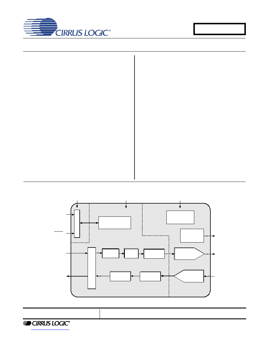
General Description
The CS4270 is a high-performance, integrated audio
CODEC. The CS4270 performs stereo analog-to-digital
(A/D) and digital-to-analog (D/A) conversion of up to
24-bit serial values at sample rates up to 216 kHz.
Standard 50/15
µ
s de-emphasis is available for sam-
pling rates of 44.1 kHz for compatibility with digital audio
programs mastered using the 50/15
µ
s pre-emphasis
technique.
Integrated level translators allow easy interfacing be-
tween the CS4270 and other devices operating over a
wide range of logic levels.
Independently addressable high-pass filters are avail-
able for the right and left channel of the A/D. This allows
the A/D to be used in a wide variety of applications
where one audio channel and one DC measurement
channel is desired.
The CS4270's wide dynamic range, negligible distor-
tion, and low noise make it ideal for applications such as
DVD-recorders, digital televisions, set top boxes, ef-
fects processors, and automotive audio systems.
ORDERING INFORMATION
Product
Description
Package
Pb-Free
Grade
Temp Range
Container
Order #
CS4270
24-Bit 192 kHz Stereo
Audio CODEC
24-TSSOP
YES
Commercial -10∞ to +85∞ C
Rail
CS4270-CZZ
Tape & Reel CS4270-CZZR
CS4270
24-Bit 192 kHz Stereo
Audio CODEC
24-TSSOP
YES
Commercial -40∞ to +85∞ C
Rail
CS4270-DZZ
Tape & Reel CS4270-DZZR
CDB4270 CS4270 Evaluation Board
-
-
-
-
-
CDB4270

DS686A1
3
CS4270
TABLE OF CONTENTS
1. PIN DESCRIPTIONS - SOFTWARE MODE ............................................................................. 6
2. PIN DESCRIPTIONS - STAND-ALONE MODE ....................................................................... 7
3. CHARACTERISTICS AND SPECIFICATIONS ........................................................................ 8
SPECIFIED OPERATING CONDITIONS ................................................................................. 8
ABSOLUTE MAXIMUM RATINGS ........................................................................................... 8
THERMAL CHARACTERISTICS.............................................................................................. 8
DAC ANALOG CHARACTERISTICS (CS4270-CZZ)............................................................... 9
DAC ANALOG CHARACTERISTICS (CS4270-DZZ)............................................................... 9
DAC COMBINED INTERPOLATION & ON-CHIP ANALOG FILTER RESPONSE................ 11
ADC ANALOG CHARACTERISTICS (CS4270-CZZ)............................................................. 12
ADC ANALOG CHARACTERISTICS (CS4270-DZZ)............................................................. 13
ADC ANALOG CHARACTERISTICS - ALL MODES ............................................................. 14
ADC DIGITAL FILTER CHARACTERISTICS ........................................................................ 14
DC ELECTRICAL CHARACTERISTICS ................................................................................ 15
DIGITAL CHARACTERISTICS............................................................................................... 16
SWITCHING CHARACTERISTICS - SERIAL AUDIO PORT................................................. 16
SWITCHING CHARACTERISTICS - I≤C MODE CONTROL PORT....................................... 19
SWITCHING CHARACTERISTICS - SPI CONTROL PORT.................................................. 20
4. TYPICAL CONNECTION DIAGRAM ..................................................................................... 21
5. APPLICATIONS ..................................................................................................................... 22
5.1 Stand-Alone Mode ........................................................................................................... 22
5.1.1 Recommended Power-Up Sequence ................................................................. 22
5.1.2 Master/Slave Mode ............................................................................................. 22
5.1.3 System Clocking ................................................................................................. 22
5.1.4 Clock Ratio Selection .......................................................................................... 23
5.1.5 Interpolation Filter .............................................................................................. 23
5.1.6 High-Pass Filter .................................................................................................. 23
5.1.7 Mode Selection & De-Emphasis ......................................................................... 24
5.1.8 Serial Audio Interface Format Selection ............................................................. 24
5.2 Control Port Mode ........................................................................................................... 24
5.2.1 Recommended Power-Up Sequence - Access to Control Port Mode ................ 24
5.2.2 Master / Slave Mode Selection ........................................................................... 24
5.2.3 System Clocking ................................................................................................. 25
5.2.4 Clock Ratio Selection .......................................................................................... 25
5.2.5 Internal Digital Loopback .................................................................................... 26
5.2.6 Auto-Mute ........................................................................................................... 26
5.2.7 High-Pass Filter and DC Offset Calibration ........................................................ 26
5.2.8 De-Emphasis ...................................................................................................... 27
5.2.9 Oversampling Modes .......................................................................................... 27
5.3 De-Emphasis Filter .......................................................................................................... 27
5.4 Analog Connections ........................................................................................................ 28
5.4.1 Input Connections ............................................................................................... 28
5.4.2 Output Connections ............................................................................................ 29
5.5 Mute Control .................................................................................................................... 29
5.6 Synchronization of Multiple Devices ................................................................................ 30
5.7 Grounding and Power Supply Decoupling ....................................................................... 30
6. CONTROL PORT INTERFACE .............................................................................................. 31
6.1 SPITM Mode ..................................................................................................................... 31
6.2 I≤C Mode .......................................................................................................................... 32
7. REGISTER QUICK REFERENCE .......................................................................................... 33
8. REGISTER DESCRIPTION .................................................................................................... 34
8.1 Chip ID - Address 01h ..................................................................................................... 34

4
DS686A1
CS4270
8.2 Power Control - Address 02h .......................................................................................... 34
8.2.1 Freeze (Bit 7) ...................................................................................................... 34
8.2.2 PDN_ADC (Bit 5) ................................................................................................ 34
8.2.3 PDN_DAC (Bit 1) ................................................................................................ 34
8.2.4 Power Down (Bit 0) ............................................................................................. 34
8.3 Mode Control - Address 03h ............................................................................................ 35
8.3.1 ADC Functional Mode & Master / Slave Mode (Bits 5:4) .................................... 35
8.3.2 Ratio Select (Bits 3:1) ......................................................................................... 35
8.3.3 PopGuard Disable (Bit 0) .................................................................................... 35
8.4 ADC and DAC Control - Address 04h ............................................................................. 35
8.4.1 ADC HPF Freeze A (Bit 7) .................................................................................. 35
8.4.2 ADC HPF Freeze B (Bit 6) .................................................................................. 36
8.4.3 Digital Loopback (Bit 5) ....................................................................................... 36
8.4.4 DAC Digital Interface Format (Bits 4:3) ............................................................... 36
8.4.5 ADC Digital Interface Format (Bit 0) ................................................................... 36
8.5 Transition Control - Address 05h ..................................................................................... 37
8.5.1 DAC Single Volume (Bit 7) .................................................................................. 37
8.5.2 Soft Ramp or Zero Cross Enable (Bits 6:5) ........................................................ 37
8.5.3 Invert Signal Polarity (Bits 4:1) ............................................................................ 37
8.5.4 De-Emphasis Control (Bit 0) ............................................................................... 38
8.6 Mute Control - Address 06h ............................................................................................. 38
8.6.1 Auto-Mute (Bit 5) ................................................................................................. 38
8.6.2 ADC Channel A & B Mute (Bits 4:3) ................................................................... 38
8.6.3 Mute Polarity (Bit 2) ............................................................................................ 38
8.6.4 DAC Channel A & B Mute (Bits 1:0) ................................................................... 38
8.7 DAC Channel A Volume Control - Address 07h .............................................................. 39
8.8 DAC Channel B Volume Control - Address 08h .............................................................. 39
10. PACKAGE DIMENSIONS .................................................................................................... 41
11. APPENDIX ....................................................................................................................... 42
12. REVISION HISTORY ............................................................................................................ 48
LIST OF FIGURES
Figure 1. Output Test Load ....................................................................................................................... 10
Figure 2. Maximum Loading ...................................................................................................................... 10
Figure 3. Master Mode Serial Audio Port Timing ...................................................................................... 17
Figure 4. Slave Mode Serial Audio Port Timing ........................................................................................ 17
Figure 5. Format 0, Left Justified up to 24-Bit Data .................................................................................. 18
Figure 6. Format 1, I≤S up to 24-Bit Data .................................................................................................. 18
Figure 7. Format 2, Right Justified 16-Bit Data. (Available in Control Port Mode only)
Format 3, Right Justified 24-Bit Data. (Available in Control Port Mode only) ............................................ 18
Figure 8. I≤C Mode Control Port Timing .................................................................................................... 19
Figure 9. SPI Control Port Timing ............................................................................................................. 20
Figure 10. CS4270 Typical Connection Diagram ...................................................................................... 21
Figure 11. De-Emphasis Curve ................................................................................................................. 27
Figure 12. CS4270 Recommended Analog Input Network ....................................................................... 28
Figure 13. CS5344 Example Analog Input Network .................................................................................. 29
Figure 14. CS4270 Recommended Analog Output Filter .......................................................................... 29
Figure 15. Suggested Active-Low Mute Circuit ......................................................................................... 30
Figure 16. Control Port Timing, SPI mode ................................................................................................ 31
Figure 17. Control Port Timing, I≤C Mode ................................................................................................. 32
Figure 18. De-Emphasis Curve ................................................................................................................. 38
Figure 19. DAC Single-Speed (fast) Stopband Rejection ......................................................................... 42
Figure 20. DAC Single-Speed (fast) Transition Band ............................................................................... 42

DS686A1
5
CS4270
Figure 21. DAC Single-Speed (fast) Transition Band (detail) ................................................................... 42
Figure 22. DAC Single-Speed (fast) Passband Ripple ............................................................................. 42
Figure 23. DAC Single-Speed (slow) Stopband Rejection ........................................................................ 42
Figure 24. DAC Single-Speed (slow) Transition Band .............................................................................. 42
Figure 25. DAC Single-Speed (slow) Transition Band (detail) .................................................................. 43
Figure 26. DAC Single-Speed (slow) Passband Ripple ............................................................................ 43
Figure 27. DAC Double-Speed (fast) Stopband Rejection ........................................................................ 43
Figure 28. DAC Double-Speed (fast) Transition Band .............................................................................. 43
Figure 29. DAC Double-Speed (fast) Transition Band (detail) .................................................................. 43
Figure 30. DAC Double-Speed (fast) Passband Ripple ............................................................................ 43
Figure 31. DAC Double-Speed (slow) Stopband Rejection ...................................................................... 44
Figure 32. DAC Double-Speed (slow) Transition Band ............................................................................. 44
Figure 33. DAC Double-Speed (slow) Transition Band (detail) ................................................................. 44
Figure 34. DAC Double-Speed (slow) Passband Ripple ........................................................................... 44
Figure 35. DAC Quad-Speed (fast) Stopband Rejection .......................................................................... 44
Figure 36. DAC Quad-Speed (fast) Transition Band ................................................................................. 44
Figure 37. DAC Quad-Speed (fast) Transition Band (detail) ..................................................................... 45
Figure 38. DAC Quad-Speed (fast) Passband Ripple ............................................................................... 45
Figure 39. DAC Quad-Speed (slow) Stopband Rejection ......................................................................... 45
Figure 40. DAC Quad-Speed (slow) Transition Band ............................................................................... 45
Figure 41. DAC Quad-Speed (slow) Transition Band (detail) ................................................................... 45
Figure 42. DAC Quad-Speed (slow) Passband Ripple ............................................................................. 45
Figure 43. ADC Single-Speed Mode Stopband Rejection ........................................................................ 46
Figure 44. ADC Single-Speed Mode Transition Band ............................................................................... 46
Figure 45. ADC Single-Speed Mode Transition Band (Detail) .................................................................. 46
Figure 46. ADC Single-Speed Mode Passband Ripple ............................................................................. 46
Figure 47. ADC Double-Speed Mode Stopband Rejection ....................................................................... 46
Figure 48. ADC Double-Speed Mode Transition Band ............................................................................. 46
Figure 49. ADC Double-Speed Mode Transition Band (Detail) ................................................................. 47
Figure 50. ADC Double-Speed Mode Passband Ripple ........................................................................... 47
Figure 51. ADC Quad-Speed Mode Stopband Rejection .......................................................................... 47
Figure 52. ADC Quad-Speed Mode Transition Band ................................................................................ 47
Figure 53. ADC Quad-Speed Mode Transition Band (Detail) ................................................................... 47
Figure 54. ADC Quad-Speed Mode Passband Ripple .............................................................................. 47
LIST OF TABLES
Table 1. Speed Modes .............................................................................................................................. 22
Table 2. Clock Ratios - Stand-Alone Mode ............................................................................................... 23
Table 3. CS4270 Stand-Alone Mode Control............................................................................................ 24
Table 4. Speed Modes .............................................................................................................................. 25
Table 5. Clock Ratios - Control Port Mode................................................................................................ 25
Table 6. Analog Input Design Parameters ................................................................................................ 28
Table 7. Memory Address Pointer............................................................................................................. 32
Table 8. Functional Mode Selection.......................................................................................................... 35
Table 9. MCLK Divider Configuration........................................................................................................ 35
Table 10. DAC Digital Interface Formats .................................................................................................. 36
Table 11. ADC Digital Interface Formats .................................................................................................. 36
Table 12. Soft Cross or Zero Cross Mode Selection................................................................................. 37
Table 13. Digital Volume Control .............................................................................................................. 39