 | –≠–ª–µ–∫—Ç—Ä–æ–Ω–Ω—ã–π –∫–æ–º–ø–æ–Ω–µ–Ω—Ç: CS4327 | –°–∫–∞—á–∞—Ç—å:  PDF PDF  ZIP ZIP |
Document Outline
- note-cry.pdf
- note-cry.pdf
1
Copyright
©
Cirrus Logic, Inc. 1997
(All Rights Reserved)
Cirrus Logic, Inc.
Crystal Semiconductor Products Division
P.O. Box 17847, Austin, Texas 78760
(512) 445 7222 FAX: (512) 445 7581
http://www.crystal.com
CS4327
Low Cost, 20-Bit, Stereo, Audio D/A Converter
Features
l
20-Bit Conversion
l
108 dB Signal-to-Noise-Ratio (EIAJ)
l
100 dB Dynamic Range
l
Single-Ended Outputs
l
Complete Stereo DAC System
- 128X Interpolation Filter
- Delta-Sigma DAC
- Analog Post Filter
l
Low Clock Jitter Sensitivity
l
Filtered Line-Level Outputs
- Linear Phase Filtering
- Zero Phase Error Between Channels
l
Digital De-emphasis for 32 kHz, 44.1 kHz &
48 kHz
Description
The CS4327 is a complete stereo digital-to-analog out-
put system. In addition to the traditional D/A function, the
CS4327 includes a digital interpolation filter followed by
an 128X oversampled delta-sigma modulator. The mod-
ulator output controls the reference voltage input to an
ultra-linear analog low-pass filter. This architecture al-
lows for infinite adjustment of sample rate between 1 and
50 kHz while maintaining linear phase response simply
by changing the master clock frequency.
The CS4327 also includes an extremely flexible serial
port utilizing mode select pins to support multiple inter-
face formats.
The master clock can be either 256, 384, or 512 times
the input sample rate, supporting various audio
environments.
ORDERING INFO
CS4327-KS
-10 to 70 ∞C
16-pin Plastic SSOP
CDB4327
CS4327 Evaluation Board
I
DIF0
DIF1
DEM0 DEM1
VA+
VD+
LRCK
SCLK
SDATA
AOUTL
MCLK
AGND
Serial Input
Interface
De-emphasis
Voltage Reference
Interpolator
Delta-Sigma
Modulator
DAC
Analog
Low-Pass
Filter
Interpolator
Delta-Sigma
Modulator
DAC
Analog
Low-Pass
Filter
AOUTR
DGND
AUTO_MUTE
7
9
10
15
11
1
2
3
6
14
13
4
8
5
12
CMFILT
16
DEC `97
DS190F1

CS4327
2
DS190F1
ANALOG CHARACTERISTICS
(T
A
= 25 ∞C; Internal SCLK; Full-Scale Output Sine wave, 997 Hz;
12.288 MHz MCLK; Fs = 48 kHz; Input Data = 20 Bits; SCLK = 3.072 MHz; R
L
= 10 k
; VD+ = VA+ = 5 V;
Logic 1 = VD+, Logic 0 = DGND; Measurement Bandwidth is 10 Hz to 20 kHz, unweighted, unless otherwise spec-
ified.)
Notes: 1. Triangular PDF Dithered Data
2. Auto-mute enabled. See parameter definitions.
3. Group Delay for Fs = 48 kHz
25/48 kHz = 520 µs
Parameter
Symbol
Min Typ
Max
Unit
Specified Temperature Operating Range
T
A
-10
-
70
∞C
Dynamic Performance
Dynamic Range
(Note 1)
20-Bit
(A-Weighted)
18-Bit
(A-Weighted)
16-Bit
(A-Weighted)
93
96
-
-
-
-
97
100
97
100
93
95
-
-
-
-
-
-
dB
dB
dB
dB
dB
dB
Total Harmonic Distortion + Noise
(Note 1)
20-Bit
0 dB
-20 dB
-60 dB
18-Bit
0 dB
-20 dB
-60 dB
16-Bit
0 dB
-20 dB
-60 dB
THD+N
-87
-
-33
-
-
-
-
-
-
-93
-77
-37
-93
-77
-37
-93
-77
-37
-
-
-
-
-
-
-
-
-
dB
dB
dB
dB
dB
dB
dB
dB
dB
Idle Channel Noise / Signal-to-Noise-Ratio
(Note 2)
-
108
-
dBFS
Interchannel Isolation
(1 kHz)
-
-105
-
dB
Combined Digital and Analog Filter Characteristics
Frequency Response 10 Hz to 20 kHz
Fs = 48 kHz
-
±0.1
-
dB
Deviation from linear phase
-
±0.5
-
deg
Passband: to -0.1 dB corner
0
-
0.4535
Fs
Passband Ripple
-
-
±0.002
dB
StopBand
0.5465
-
-
Fs
StopBand Attenuation
72
-
-
dB
Group Delay
(Note 3)
-
25/Fs
-
s
De-emphasis Error
-
-
±0.2
dB

CS4327
DS190F1
3
ANALOG CHARACTERISTICS
(Continued)
POWER AND THERMAL CHARACTERISTICS
(T
A
= 25 ∞C; Internal SCLK; Full-Scale Output
Sine wave, 997 Hz; 12.288 MHz MCLK; Fs = 48 kHz; Input Data = 20 Bits; SCLK = 3.072 MHz; R
L
= 10 k
;
VD+ = VD+ = 5 V; Logic 1 = VD+, Logic 0 = DGND; Measurement Bandwidth is 10 Hz to 20 kHz, unweighted,
unless otherwise specified.)
Parameter
Symbol
Min Typ
Max
Unit
dc Accuracy
Interchannel Gain Mismatch
-
0.1
-
dB
Gain Error
-
±2
±5
%
Gain Drift
-
200
-
ppm/∞C
Analog Output
Full Scale Output Voltage
0.95
1.0
1.05
Vrms
Load Resistance
6
-
-
k
Load Capacitance
-
-
100
pF
Output Common Mode Voltage
-
2.3
-
V
Parameter
Symbol Min Typ
Max
Unit
Power Supply Current
Normal Operation
Power Down
IA+
ID+
(IA+) + (ID+)
(IA+) + (ID+)
-
-
-
-
25
12
37
300
-
-
43
-
mA
mA
mA
µA
Power Dissipation
Normal Operation
Power-down
-
-
185
1.5
215
-
mW
mW
Power Supply Rejection Ratio (1 kHz)
PSRR
-
60
-
dB
Allowable Junction Temperature
-
-
135
∞C
Junction to Ambient Thermal Impedance
JA
-
120
-
∞C/W

CS4327
4
DS190F1
SWITCHING CHARACTERISTICS
(T
A
= 25 ∞C; VA+ = 5.0 V; Inputs: Logic 0 = 0 V, Logic 1 = VD+,
C
L
= 20 pF)
Parameter
Symbol Min Typ
Max
Unit
Input Sample Rate
Fs
1
-
50
kHz
MCLK Pulse Width High
MCLK/LRCK = 512
10
-
-
ns
MCLK Pulse Width Low
MCLK/LRCK = 512
10
-
-
ns
MCLK Pulse Width High
MCLK/LRCK = 384
21
-
-
ns
MCLK Pulse Width Low
MCLK/LRCK = 384
21
-
-
ns
MCLK Pulse Width High
MCLK/LRCK = 256
31
-
-
ns
MCLK Pulse Width Low
MCLK/LRCK = 256
31
-
-
ns
External SCLK Mode
SCLK Pulse Width Low
t
sclkl
20
-
-
ns
SCLK Pulse Width High
t
sclkh
20
-
-
ns
SCLK Period
t
sclkw
-
-
ns
SCLK rising to LRCK edge delay
t
slrd
20
-
-
ns
SCLK rising to LRCK edge setup time
t
slrs
20
-
-
ns
SDATA valid to SCLK rising setup time
t
sdlrs
20
-
-
ns
SCLK rising to SDATA hold time
t
sdh
20
-
-
ns
Internal SCLK Mode
SCLK Period
SCLK/LRCK = 64
t
sclkw
-
-
ns
SCLK rising to LRCK edge
t
sclkr
-
-
ns
SDATA valid to SCLK rising setup time
t
sdlrs
-
-
ns
SCLK rising to SDATA hold time
MCLK/LRCK = 256 or 512
t
sdh
-
-
ns
SCLK rising to SDATA hold time
MCLK/LRCK = 384
t
sdh
-
-
ns
1
128(Fs)
--------------------
1
64(Fs)
-----------------
t
sc lk w
2
------------------
1
512(Fs)
--------------------
10
+
1
512(Fs)
--------------------
15
+
1
384(Fs)
--------------------
15
+

CS4327
DS190F1
5
sclkh
t
slrs
t
slrd
t
sdlrs
t
sdh
t
sclkl
t
SDATA
SCLK
LRCK
SDATA
*INTERNAL SCLK
LRCK
sclkw
t
sdlrs
t
sdh
t
sclkr
t
External Serial Mode Input Timing
Internal Serial Mode Input Timing.
*
The SCLK pin must be terminated to ground.
The SCLK pulses shown are internal to the CS4327

CS4327
6
DS190F1
DIGITAL CHARACTERISTICS
(T
A
= 25 ∞C; VD+ = 5 V ±5%)
ABSOLUTE MAXIMUM RATINGS
(AGND = DGND = 0 V; all voltages with respect to ground.)
WARNING: Operation at or beyond these limits may result in permanent damage to the device.
Normal operation is not guaranteed at these extremes.
RECOMMENDED OPERATING CONDITIONS
(AGND = DGND = 0 V; all voltages with respect to ground.)
Parameter
Symbol Min Typ
Max
Unit
High-Level Input Voltage
V
IH
2.0
-
-
V
Low-Level Input Voltage
V
IL
-
-
0.8
V
Input Leakage Current
-
-
±10.0
µA
Digital Input Capacitance
-
10
-
pF
Parameter
Symbol
Min
Max
Unit
DC Power Supply:
Positive Analog
Positive Digital
|VA+ - VD+|
VA+
VD+
-0.3
-0.3
0.0
6.0
6.0
0.4
V
V
V
Input Current, Any Pin Except Supplies
I
in
-
±10
mA
Digital Input Voltage
V
IND
-0.3
(VD+) + 0.4
V
Ambient Operating Temperature (power applied)
T
A
-55
125
∞C
Storage Temperature
T
stg
-65
150
∞C
Parameter
Symbol Min Typ
Max
Unit
DC Power Supply:
Positive Analog
Positive Digital
|VA+ - VD+|
VA+
VD+
4.75
4.75
-
5.0
5.0
-
5.25
5.25
0.1
V
V
V

CS4327
DS190F1
7
SCLK*
Audio
Data
Processor
External Clock
MCLK
AGND
AOUTR
CS4327
SDATA
VA+
+5 V
Analog
2
0.1 µF
+
1 µF
DEM0
DEM1
Mode
Select
DIF1
DIF0
AOUTL
DGND
VD+
AUTO_MUTE
6
3
4
5
8
12
2
1
10
9
7
11
15
LRCK
* SCLK must be connected to DGND
for operation in Internal SCLK Mode
CMFILT
16
1 µF
ANALOG
FILTER
ANALOG
FILTER
14
13
+
0.1 µF
+ 1 µF
Figure 1. Typical Connection Diagram

CS4327
8
DS190F1
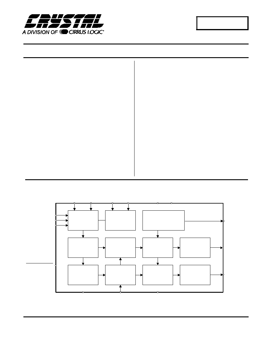
GENERAL DESCRIPTION
The CS4327 is a complete stereo digital-to-analog
system including digital interpolation, 128x fourth-
order delta-sigma digital-to-analog conversion, and
analog filtering, see Figure 2. This architecture pro-
vides a high insensitivity to clock jitter. The DAC
converts digital data at any input sample rate be-
tween 1 and 50 kHz, including the standard audio
rates of 48, 44.1 and 32 kHz.
The primary purpose of using delta-sigma modula-
tion techniques is to avoid the limitations of laser
trimmed resistive DAC architectures by using an
inherently linear 1-bit DAC. The advantages of a 1-
bit DAC include: ideal differential linearity, no dis-
tortion mechanisms due to resistor matching errors
and no linearity drift over time and temperature due
to variations in resistor values.
Digital Interpolation Filter
The digital interpolation filter increases the sample
rate by a factor of 4 and is followed by a 32x digital
sample-and-hold to effectively achieve a 128x in-
terpolation filter. This filter eliminates images of
the baseband audio signal which exist at multiples
of the input sample rate, Fs. This allows for the se-
lection of a less complex analog filter based on out-
of-band noise attenuation requirements rather than
anti-image filtering. Following the interpolation
filter, the resulting frequency spectrum has images
of the input signal at multiples of 128x the input
sample rate. These images are removed by the ex-
ternal analog filter.
Delta-Sigma Modulator
The interpolation filter is followed by a fourth-or-
der delta-sigma modulator which converts the 24-
bit interpolation filter output into 1-bit data at 128x
Fs.
Switched-Capacitor Filter
The delta-sigma modulator is followed by a digital-
to-analog converter which translates the 1-bit data
into a series of charge packets. The magnitude of
the charge in each packet is determined by sam-
pling of a voltage reference onto a switched capac-
itor, where the polarity of each packet is controlled
by the 1-bit signal. This technique greatly reduces
the sensitivity to clock jitter and is a major im-
provement over earlier generations of 1-bit digital-
to-analog converters where the magnitude of
charge in the D-to-A process is determined by
switching a current reference for a period of time
defined by the master clock.
SYSTEM DESIGN
Master Clock
The Master Clock, MCLK, is used to operate the
digital interpolation filter and the delta-sigma mod-
ulator. MCLK must be either 256x, 384x or 512x
the desired Input Sample Rate, Fs. Fs is the fre-
quency at which digital audio samples for each
channel are input to the DAC and is equal to the
LRCK frequency. The MCLK to LRCK frequency
ratio is detected automatically during the initializa-
tion sequence by counting the number of MCLK
Interpolator
Delta-Sigma
Modulator
DAC
Analog
Low-Pass
Filter
AOUT
Figure 2. Block Diagram

CS4327
DS190F1
9
transitions during a single LRCK period. Internal
dividers are then set to generate the proper clocks
for the digital filter, delta-sigma modulator and
switched-capacitor filter. Once the MCLK to
LRCK frequency ratio has been detected, the phase
and frequency relationship between the two clocks
must remain fixed. If during any LRCK this rela-
tionship is changed, the CS4327 will reset. Table 1
illustrates the standard audio sample rates and the
required MCLK frequencies.
Table 1. Common Clock Frequencies
Serial Data Interface
The serial data interface is accomplished via the se-
rial data input, SDATA, serial data clock, SCLK,
and the left/right clock, LRCK. The CS4327 sup-
ports four serial data formats which are selected via
the digital input format pins DIF0 and DIF1. The
different formats control the relationship of LRCK
to the serial data and the edge of SCLK used to
latch the data into the input buffer. Table 2 lists the
formats, along with the associated figure number.
The serial data is represented in 2's-complement
format with the MSB-first in all four formats.
Table 2. Digital Input Formats
Formats 0 and 1 are shown in Figure 3. The audio
data is right-justified, LSB aligned with the trailing
edge of LRCK, and latched into the serial input
data buffer on the rising edge of SCLK. Formats 0
and 1 are 16 and 20-bit versions and differ only in
the number of data bits required.
Format 2 is 20-bit left justified, MSB aligned with
the leading edge of LRCK. Data is latched on the
falling edge of SCLK. The format will support 16
and 18-bit inputs if the data is followed by four or
two zeros to simulate a 20-bit input as shown in
Figure 4. A very small offset will result if the 18 or
16-bit data is followed by static non-zero data.
Format 3 is compatible with the I
2
S serial data pro-
tocol as shown in Figure 5. Notice that the MSB is
delayed 1 period of SCLK following the leading
edge of LRCK and LRCK is inverted compared to
the previous formats. Data is latched on the rising
edge of SCLK. Format 3 is a 20-bit I
2
S format. 18-
bit or 16-bit I
2
S can be implemented if the data is
followed by two or four zeros to simulate a 20-bit
input as shown in Figure 5. A very small offset will
result if the 18 or 16-bit data is followed by static
non-zero data.
Serial Clock
The serial clock controls the shifting of data into
the input data buffers. The CS4327 supports both
external and internal serial clock generation modes.
External Serial Clock
The CS4327 will enter the external serial clock
mode if 15 or more high\low transitions are detect-
ed on the SCLK pin during any phase of the LRCK
period. When this mode is enabled, internal serial
clock mode cannot be accessed without returning
to the power down mode.
Internal Serial Clock
In the Internal Serial Clock Mode, the serial clock
is internally derived and synchronous with MCLK.
The internal SCLK / LRCK ratio is always 64 and
operation in this mode is identical to operation with
an external serial clock synchronized with LRCK.
The SCLK pin must be connected to DGND for
proper operation.
The internal serial clock mode is advantageous in
that there are situations where improper serial
Fs
(kHz)
MCLK (MHz)
256x
384x
512x
32
8.1920
12.2880
16.3840
44.1
11.2896
16.9344
22.5792
48
12.2880
18.4320
24.5760
DIF1
DIF0
Format
Figure
0
0
0
3
0
1
1
3
1
0
2
4
1
1
3
5

CS4327
10
DS190F1
LRCK
SCLK
Left Channel
SDATA
Format 0
6 5 4 3 2 1 0
9 8 7
15 14 13 12 11 10
1
6 5 4 3 2 1 0
9 8 7
15 14 13 10
6 5 4 3 2 1 0
9 8 7
15 14 13 12 11 10
1 0
6 5 4 3 2 1 0
9 8 7
17 16 15 14 13 10
17 16
19 18
SDATA
Format 1
19 18
Right Channel
0
6
LRCK
SCLK
Left Channel
Right Channel
SDATA
16-Bit
6 5 4 3 2 1 0
9 8 7
15 14 12 11 10
6 2 1 0
2
9 8 7
15 14 13 12 11 10
SDATA
18-Bit
8 7 6 5 4 3 2
11 10 9
17 16
13 12
3 2
4
1 0
9 8 4
15 14 13 12 11 10
1 0
17 16
15
17
SDATA
20-Bit
10 9 8 7 6 5 4
13 12 11
19 18
15 14
5 4 3 2 1
11 10 6
17 16 15 14 13 12
3
19 18
19
2 1
0
6
6
2
48
10
0
6
LRCK
SCLK
Left Channel
SDATA
16-Bit
6 5 4 3 2 1 0
9 8 7
15 12 11 10
6 2 1 0
2
10 9 8
15 14 13 12 11
SDATA
18-Bit
8 7 6 5 4 3 2
11 10 9
17
13 12
3 2
4
1
8 4
16 15 14 13 12 11
1 0
17
SDATA
20-Bit
10 9 8 7 6 5 4
13 12 11
19
15 14
5 4 3 2 1
12 10 6
18 17 16 15 14 13
3
19
2 1 0
6
6
2
48
10
10
Right Channel
0
0
Figure 3. Digital Input Format 0 and 1.
Figure 4. Digital Input Format 2.
Figure 5. Digital Input Format 3.

CS4327
DS190F1
11
clock routing on the printed circuit board can de-
grade system performance. The use of the internal
serial clock mode simplifies the routing of the
printed circuit board by allowing the serial clock
trace to be deleted and avoids possible interference
effects.
Auto Mute
An auto-mute function is useful for applications,
such as compact disk players, where the idle chan-
nel noise must be minimized. The CS4327 will au-
tomatically initiate a mute for an idle channel input,
where idle channel is defined as an input of static
1's or static 0's during 8192 consecutive LRCK cy-
cles. The mute will be immediately released when
non-idle channel data is applied to either the Left or
Right channels. This feature is selectable and active
only if the AUTO_MUTE pin is low.
De-Emphasis
Implementation of digital de-emphasis requires re-
configuration of the digital filter to maintain the fil-
ter response shown in Figure 6 at multiple sample
rates. The CS4327 is capable of digital de-empha-
sis for 32, 44.1 or 48 kHz sample rates. Table 3
shows the de-emphasis control inputs for DEM 0
and DEM 1.
Table 3. De-Emphasis Filter Selection
Initialization, Calibration and Power-Down
Upon initial power-up, the DAC enters the power-
down mode. The interpolation filters and delta-sig-
ma modulators are reset, and the internal voltage
reference, one-bit D/A converters and switched-ca-
pacitor low-pass filters are powered down. The de-
vice will remain in the power-down mode until
MCLK and LRCK are presented. Once MCLK and
LRCK are detected, MCLK occurrences are count-
ed over one LRCK period to determine the MCLK
/ LRCK frequency ratio. Power is applied to the in-
ternal voltage reference, the D/A converters,
switched-capacitor filters and the DAC will begin a
common mode bias voltage calibration. This ini-
tialization and calibration sequence requires ap-
proximately 2700 cycles of LRCK. The CS4327
will enter the power-down mode, within 1 period of
LRCK, if either MCLK or LRCK is removed. The
initialization sequence, as described above, occurs
when MCLK and LRCK are restored.
An offset calibration can be invoked by changing
the state of Digital Input Format pins, DIF0 and/or
DIF1, for at least 3 LRCK cycle. During calibra-
tion, a common-mode voltage of approximately
1.8 V appears at the outputs, with approximately a
16 kohm output impedance. Following calibration,
the analog output impedance becomes less than
10 ohms and the common mode voltage will move
to approximately 2.3 V.
Gain
dB
-10 dB
0 dB
Frequency
T2 = 15
µ
s
T1=50
µ
s
F1
3.183 kHz
F2
10.61 kHz
Figure 6. De-emphasis Filter Response
DEM1
DEM0
De-emphasis
0
0
32 kHz
0
1
44.1 kHz
1
0
48 kHz
1
1
OFF

CS4327
12
DS190F1
Combined Digital and Analog Filter
Response
The frequency response of the combined analog
switched-capacitor and digital filters is shown in
Figures 7, 8, and 9. The overall response is clock
dependent and will scale with Fs. Note that the re-
sponse plots have been normalized to Fs and can be
de-normalized by multiplying the X-axis scale by
Fs, such as 48 kHz.
Figure 7. CS4327 Combined Digital and Analog Filter
Stopband Rejection
Figure 8. CS4327 Combined digital and Analog Filter
Passband Response
Figure 9. CS4327 Combined Digital and Analog Filter
Transition Band

CS4327
DS190F1
13
Analog Output and Filtering
The CS4327 contains an on-chip buffer amplifier
producing single-ended outputs. Each output will
produce a nominal 2.83 Vpp (1 Vrms) output with
a 2.3 volt common mode for a full scale digital in-
put.
The CS4327 filter is a linear phase design and does
not include phase or amplitude compensation for
an external filter. Therefore, the DAC system phase
and amplitude response will be dependent on the
external analog circuitry. The second-order low-
pass filter with a -3 dB frequency of 50 kHz shown
in Figure 10 will give good results in most applica-
tions. The design of this filter is discussed in AN55,
the Crystal Applications Note "Design Notes for a
2-pole Filter." Figure 11 displays the the output
spectrum of the CS4327. Figure 12 displays the
output spectrum following the 2-pole filter. Notice
the attenuation beyond 50 kHz.
_
150 pF
3.4k
10k
100 pF
+
20k
Figure 10. 2-pole Butterworth Fillter
Figure 11. CS4327 Output Spectrum
Fs = 48 kHz
Figure 12. 2-pole Filtered Output Spectrum
Fs = 48 kHz

CS4327
14
DS190F1
Grounding and Power Supply Decoupling
As with any high resolution converter, the CS4327
requires careful attention to power supply and
grounding arrangements to optimize performance.
Figure 1 shows the recommended power arrange-
ments with VA+ connected to a clean +5 volt sup-
ply. VD+ should be derived from VA+ through a
2 ohm resistor. VD+ should not be used to power
additional digital circuitry. All mode pins which re-
quire VD+ should be connected to pin 6 of the
CS4327. All mode pins which require DGND
should be connected to pin 5 of the CS4327. Pins 4
and 5, AGND and DGND, should be connected to-
gether at the CS4327. DGND for the CS4327
should not be confused with the ground for the dig-
ital section of the system. The CS4327 should be
positioned over the analog ground plane near the
digital / analog ground plane split. The analog and
digital ground planes must be connected elsewhere
in the system. The CS4327 evaluation board,
CDB4327, demonstrates this layout technique.
This technique minimizes digital noise and insures
proper power supply matching and sequencing.
Decoupling capacitors should be located as near to
the CS4327 as possible.
Performance Plots
The following collection of CS4327 measurement
plots were taken from the CDB4327 evaluation
board using the Audio Precision Dual Domain Sys-
tem One.
Figure 13 shows the frequency response at a
48 kHz sample rate. The response is flat to 20 kHz
±0.1 dB as specified.
Figure 14 shows THD+N versus signal amplitude
for a 1 kHz 20-bit dithered input signal. Notice that
the there is no increase in distortion as the signal
level decreases. This indicates very good low-level
linearity, one of the key benefits of delta-sigma
digital to analog conversion.
Figure 15 shows a 16k FFT of a 1 kHz full-scale in-
put signal. The signal has been filtered by a notch
filter within the System One to remove the funda-
mental component of the signal. This minimizes
the distortion created in the analyzer analog-to-dig-
ital converter. This technique is discussed by Audio
Precision in the 10th anniversary addition of AU-
DIO.TST.
Figure 16 shows a 16k FFT of a 1 kHz -20 dBFS in-
put signal. The signal has been filtered by a notch
filter within the System One to remove the funda-
mental component of the signal.
Figure 17 shows a 16k FFT of a 1 kHz -60 dBFS in-
put signal.
Figure 18 shows the fade-to-noise linearity. The in-
put signal is a dithered 20-bit 500 Hz sine wave
which fades from -60 to -120 dBFS. During the
fade, the output from the CS4327 is measured and
compared to the ideal level. Notice the very close
tracking of the output level to the ideal, even at low
level inputs. The gradual shift of the plot away
from zero at signals levels < -110 dB is caused by
the background noise starting to dominate the mea-
surement.

CS4327
DS190F1
15
Figure 13. Frequency Response
Figure 14. THD+N vs. Amplitude
Figure 15. 0 dBFS FFT
Figure 16. -20 dBFS FFT
Figure 17. -60 dBFS FFT
Figure 18. Fade-to-Noise Linearity

CS4327
16
DS190F1
PIN DESCRIPTIONS
Power Supply Connections
VA+ - Positive Analog Power, PIN 3.
Positive analog supply. Nominally +5 volts.
VD+ - Positive Digital Power, PIN 6.
Positive supply for the digital section. Nominally +5 volts.
AGND - Analog Ground, PIN 4.
Analog ground reference.
DGND - Digital Ground, PIN 5.
Ground for the digital section.
Analog Outputs
AOUTR - Right Channel Analog Output, PIN 13.
Analog output connection for the Right channel output. Nominally 1 Vrms for full-scale digital
input signal.
AOUTL - Left Channel Analog Output, PIN 14.
Analog output connection for the Left channel outputs. Nominally 1 Vrms for full-scale digital
input signal.
1
2
3
4
5
6
7
8
9
10
11
12
13
14
15
16
CMFILT
DIF0
AOUTL
AOUTR
AUTO_MUTE
DIF1
SDATA
SCLK
MCLK
LRCK
VD+
DGND
AGND
VA+
DEM1
DEM0

CS4327
DS190F1
17
Digital Inputs
MCLK - Clock Input, PIN 8.
The frequency must be either 256x, 384x or 512x the input sample rate (Fs).
LRCK - Left/Right Clock, PIN 7.
This input determines which channel is currently being input on the Serial Data Input pin,
SDATA. The format of LRCK is controlled by DIF0 and DIF1.
SCLK - Serial Bit Input Clock, PIN 9.
Clocks the individual bits of the serial data in from the SDATA pin. The edge used to latch
SDATA is controlled by DIF0 and DIF1.
SDATA - Serial Data Input, PIN 10.
Two's complement MSB-first serial data of either 16, 18 or 20 bits is input on this pin. The
data is clocked into the CS4327 via the SCLK clock, and the channel is determined by the
LRCK clock. The format for the previous two clocks is determined by the Digital Input Format
pins, DIF0 and DIF1.
DIF0, DIF1 - Digital Input Format, PINS 15, 11
These two pins select one of four formats for the incoming serial data stream. These pins set
the format of the SCLK and LRCK clocks with respect to SDATA. The formats are listed in
Table 2.
DEM0, DEM1 - De-Emphasis Select, PINS 1, 2.
Controls the activation of the standard 50/15 µs de-emphasis filter for either 32, 44.1 or 48 kHz
sample rates.
AUTO_MUTE - Automatic Mute on Idle Channel Input, PIN 12.
When AUTO_MUTE is low the analog outputs are muted following an idle channel detection.
Idle channel is defined as an input of static 1's or static 0's during 8192 consecutive LRCK
cycles. Mute is canceled with the return of active channel input data.
CMFILT - Common Mode Filter, PIN 16
Used to filter the common mode output voltage with a 1 µF capacitor. This pin is not intended
to supply any current and should not be used for the generation of an external bias voltage.

CS4327
18
DS190F1
PARAMETER DEFINITIONS
Dynamic Range
The ratio of the full scale rms value of the signal to the rms sum of all other spectral
components over the specified bandwidth. Dynamic range is a signal-to-noise measurement
over the specified bandwidth made with a -60 dBFS signal. 60 dB is then added to the resulting
measurement to refer the measurement to full scale. This technique ensures that the distortion
components are below the noise level and do not effect the measurement. This measurement
technique has been accepted by the Audio Engineering Society, AES17-1991, and the
Electronic Industries Association of Japan, EIAJ CP-307.
Total Harmonic Distortion + Noise
The ratio of the rms value of the signal to the rms sum of all other spectral components over
the specified bandwidth (typically 10 Hz to 20 kHz), including distortion components.
Expressed in decibels.
Idle Channel Noise / Signal-to-Noise-Ratio
The ratio of the rms analog output level with 1 kHz full scale digital input to the rms analog
output level with all zeros into the digital input. Measured A-weighted over a 10 Hz to 20 kHz
bandwidth. Units in decibels. This specification has been standardized by the Audio
Engineering Society, AES17-1991, and referred to as Idle Channel Noise. This specification has
also been standardized by the Electronic Industries Association of Japan, EIAJ CP-307, and
referred to as Signal-to-Noise-Ratio.
Interchannel Isolation
A measure of crosstalk between the left and right channels. Measured for each channel at the
converter's output with all zeros to the input under test and a full-scale signal applied to the
other channel. Units in decibels.
Frequency Response
A measure of the amplitude response variation from 10 Hz to 20 kHz relative to the amplitude
response at 1 kHz. Units in decibels.
De-Emphasis Error
A measure of the difference between the ideal de-emphasis filter and the actual de-emphasis
filter response. Measured from 10 Hz to 20 kHz. Units in decibels.
Interchannel Gain Mismatch
The gain difference between left and right channels. Units in decibels.
Gain Error
The deviation from the nominal full scale analog output for a full scale digital input.
Gain Drift
The change in gain value with temperature. Units in ppm/∞C.

CS4327
DS190F1
19
PACKAGE DIMENSIONS
E
A
A1
D
E1
A2
1
1
SIDE VIEW
END VIEW
TOP VIEW
Seating
Plane
N
1
3
2
SSOP Package
Dimensions
N
MILLIMETERS
MIN NOM MAX
20
28
6.90 7.20 7.50
9.90 10.20 10.50
Note
1
1
DIM
MILLIMETERS
MIN NOM MAX
A
A1
A2
b
D
E1
e
E
L
N
-
-
2.13
0.05
0.15 0.25
1.62 1.75 1.88
0.22
0.30 0.38
see other table
5.00 5.30 5.60
7.40 7.80 8.20
0.63 0.90 1.03
see other table
0∞
4∞
8∞
Note
2, 3
1
1
e
b
2
0.61 0.65 0.69
L
INCHES
MIN NOM MAX
-
-
0.084
0.002 0.006 0.010
0.064 0.070 0.074
0.009 0.012 0.015
see other table
0.197 0.209 0.220
0.291 0.307 0.323
0.025 0.035 0.040
see other table
0∞
4∞
8∞
0.024 0.026 0.027
D
INCHES
MIN NOM MAX
0.272 0.283 0.295
0.390 0.402 0.413
NOTES:
1. DIMENSIONS D AND E1 ARE REFERENCE DATUMS
AND DO NOT INCLUDE MOLD FLASH OR
PROTRUSIONS, BUT DO INCLUDE MOLD MISMATCH
AND ARE MEASURED AT THE PARTING LINE. MOLD
FLASH OR PROTRUSIONS SHALL NOT EXCEED
0.20mm PER SIDE.
2. DIMENSION b DOES NOT INCLUDE DAMBAR
PROTRUSION/INTRUSION. ALLOWABLE DAMBAR
PROTRUSION SHALL BE 0.13mm TOTAL IN EXCESS OF
b DIMENSION AT MAXIMUM MATERIAL CONDITION.
DAMBAR INTRUSION SHALL NOT REDUCE DIMENSION
b BY MORE THAN 0.07mm AT LEAST MATERIAL
CONDITION.
3. THESE DIMENSIONS APPLY TO THE FLAT SECTION
OF THE LEAD BETWEEN 0.10 AND 0.25mm FROM LEAD
TIPS.
16
5.90 6.20 6.50
1
0.232 0.244 0.256

∑ Notes ∑

Features
∑
Demonstrates recommended layout
and grounding arrangements
∑
CS8412 Receives AES/EBU, S/PDIF,
& EIAJ-340 Compatible Digital Audio
∑
Digital and Analog Patch Areas
∑
Requires only a digital signal source
and power supplies for a complete
Digital-to-Analog-Converter system
General Description
The CDB4327 evaluation board is an excellent means
for quickly evaluating the CS4327 20-bit, stereo D/A
converter. Evaluation requires an analog signal ana-
lyzer, a digital signal source and a power supply.
Analog outputs are provided via RCA connectors for
both channels.
The CS8412 digital audio receiver I.C. provides the
system timing necessary to operate the CS4327 and
will accept AES/EBU, S/PDIF, and EIAJ-340 compat-
ible audio data. The evaluation board may also be
configured to accept external timing signals for opera-
tion in a user application during system development.
ORDERING INFORMATION:
CDB4327
Evaluation Board for CS4327
CDB4327
I/O for
Clocks
and Data
CS8412
Digital
Audio
Interface
CS4327
Analog
Filter
Copyright
©
Cirrus Logic, Inc. 1997
(All Rights Reserved)
Cirrus Logic, Inc.
Crystal Semiconductor Products Division
P.O. Box 17847, Austin, Texas 78760
(512) 445 7222 FAX: (512) 445 7581
http://www.crystal.com
DEC '95
DS190DB1
21

CDB4327 System Overview
The CDB4327 evaluation board is an excellent
means of quickly evaluating the CS4327. The
CS8412 digital audio interface receiver provides
an easy interface to digital audio signal sources
including the majority of digital audio test equip-
ment. The evaluation board also allows the user
to supply clocks and data through a 10-pin
header for system development.
The CDB4327 schematic has been partitioned
into 7 schematics shown in Figures 2 through 8.
Each partitioned schematic is represented in the
system diagram shown in Figure 1. Notice that
the the system diagram also includes the inter-
connections between the partitioned schematics.
CS4327 Digital to Analog Converter
A description of the CS4327 is included in the
CS4327 data sheet.
CS8412 Digital Audio Receiver
The system receives and decodes the standard
S/PDIF data format using a CS8412 Digital
Audio Receiver, Figure 8. The outputs of the
CS8412 include a serial bit clock, serial data,
left-right clock (FSYNC), de-emphasis control
and a 256Fs master clock. The operation of the
CS8412 and a discussion of the digital audio in-
te rface a re inc lud ed in t he 19 94 Crystal
Semiconductor Audio Data Book.
During normal operation, the CS8412 operates in
the Channel Status mode where the LED's dis-
play channel status information for the channel
selected by the CSLR/FCK jumper. This allows
the CS8412 to decode and supply the de-empha-
sis bit from the digital audio interface for control
of the CS4327 de-emphasis filter via pin 3,
CC/F0, of the CS8412.
When the Error Information Switch is activated,
the CS8412 operates in the Error and Frequency
information mode. The information displayed by
the LED's can be decoded by consulting the
CS8412 data sheet. If the Error Information
Switch is activated, the CC/F0 output has no re-
lation to the de-emphasis bit and it is likely that
the de-emphasis control for the CS4327 will be
erroneous and produce an incorrect audio output.
Encoded sample frequency information can be
displayed provided a proper clock is being ap-
plied to the FCK pin of the CS8412. When an
LED is lit, this indicates a "1" on the corre-
sponding pin located on the CS8412. When an
LED is off, this indicates a "0" on the corre-
sponding pin. Neither the L or R option of
CSLR/FCK should be selected if the FCK pin is
being driven by a clock signal.
The evaluation board has been designed such
that the input can be either optical or coax, Fig-
ure 7. It is not necessary to select the active
input. However, both inputs can not be driven
simultaneously.
Data Format
The CS4327 must be configured to be compat-
ible with the incoming data and can be set with
DIF0 and DIF1. The CS8412 data format can be
set with the M0, M1, M2 and M3. There are sev-
eral data formats which the CS8412 can produce
that are compatible with CS4327. Refer to Table
2 for one possibility.
Power Supply Circuitry
Power is supplied to the evaluation board by
four binding posts, Figure 9. The +5 Volt input
supplies power to the CS4327 (through VA+),
the CS8412 (through VA+ and VD+), and the +5
Volt digital circuitry (through VD+). The +/- 12
Volt input supplies power to the analog filter cir-
cuitry.
CDB4327
22
DS190DB1

Input/Output for Clocks and Data
The evaluation board has been designed to allow
the interface to external systems via the 10-pin
header, J1. This header allows the evaluation
board to accept externally generated clocks and
data. The schematic for the clock/data I/O is
shown in Figure 6. The 74HC243 transceiver
functions as an I/O buffer where the CLK
SOURCE jumper determines if the transceiver
operates as a transmitter or receiver.
The transceiver operates as a transmitter with the
CLK SOURCE jumper in the 8412 position.
LRCK, SDATA, and SCLK from the CS8412
will be available on J1. J22 must be in the 0
position and J23 must be in the 1 position for
MCLK to be an output and to avoid bus conten-
tion on MCLK.
The transceiver operates as a receiver with the
CLK SOURCE jumper in the EXTERNAL posi-
tion. LRCK, SDATA and SCLK on J1 become
inputs. The CS8412 must be removed from the
evaluation board for operation in this mode.
There are 2 options for the source of MCLK in
the EXT CLK source mode. MCLK can be an
input with J23 in the 1 position and J22 in the 0
position. However, the recommended mode of
operation is to generate MCLK on the evaluation
board. MCLK becomes an output with LRCK,
SCLK and SDATA inputs. This technique insures
that the CS4327 receives a jitter free clock to
maximize performance. This can be accom-
plished by installing a crystal oscillator into U4,
see Figure 8 (the socket for U4 is located within
the footprint for the CS8412) and placing J22 in
the 1 position and J23 in the 0 position.
Analog Filter
The design of the second-order Butterworth low-
pass filter, Figure 5, is discussed in the CS4327
data sheet and the applications note "Design
Notes for a 2-pole Filter."
Grounding and Power Supply Decoupling
The CS4327 requires careful attention to power
supply and grounding arrangements to optimize
performance. Figure 2 shows the recommended
power arrangements with VA+ connected to a
clean +5 Volt supply. VD1+ is derived from VA+
through a 2 ohm resistor. VD1+ should not used
for any additional digital circuitry.
Ideally, all mode pins which require VD1+
should be connected to pin 6 of the CS4327 and
all mode pins which require DGND should con-
nected to pin 5 of the CS4327. AGND and
DGND, Pins 4 and 5, are connected together at
the CS4327. The evaluation board has separate
analog and digital regions with individual
ground planes. DGND for the CS4327 should
not be confused with the ground for the digital
section of the system (GND). The CS4327 is po-
sitioned over the analog ground plane near the
digital/analog ground plane split. These ground
planes are connected elsewhere on the board.
This layout technique is used to minimizing digi-
tal noise and to insure proper power supply
matching/sequencing. The decoupling capacitors
are located as close to the CS4327 as possible.
Extensive use of ground plane fill on both the
analog and digital sections of the evaluation
board yield large reductions in radiated noise ef-
fects.
CDB4327
DS190DB1
23
JUMPER
PURPOSE
POSITION
FUNCTION SELECTED
CSLR/FCK
Selects channel for
CS8412 channel status
information
L
See CS8412 data sheet for details
R
Clock Select
Selects source of system
clocks and data
*8412
CS8412 clock/data source
EXT
External clock/data source
J22
J23
Selects MCLK as
input or output
0
1
See
Input/Output for Clocks and
Data section of text
M0
CS8412 mode select
*Low
See CS8412 data sheet for details
M1
*Low
M2
*Low
M3
*Low
auto_mute
CS4327 Auto Mute
*Low
On
High
Off
DEM0
DEM1
De-emphasis select
*High
See CS4327 data sheet for details
*Low
set for 44.1 kHz
DIF0
CS4327 digital input
*Low
See CS4327 data sheet for details
DIF1
format
*High
SCLK
CS4327 SCLK Mode
*INT
Internal SCLK Mode
EXT
External SCLK Mode
DEM_8412
Selects source of de-
emphasis control
*Low
CS8412 de-emphasis
High
De-emphasis input static high
* Default setting from factory
Table 2. CDB4327 Jumper Selectable Options
CONNECTOR
INPUT/OUTPUT
SIGNAL PRESENT
+5V
input
+5 Volts for the CS4327, CS8412, and digital
section
+/- 12V
input
+/- 12 Volts for analog filter section
GND
input
ground connection from power supply
Digital input
input
digital audio interface input via coax
Optical input
input
digital audio interface input via optical
J1
input/output
I/O for system clocks and digital audio data
AOUTL
output
left channel analog output
AOUTR
output
right channel analog output
Table 1. System Connections
CDB4327
24
DS190DB1

Digital
Audio
Input
I/O for
Clocks
and Data
CS8412
Digital
Audio
Interface
RX
N
RX
P
MCLK
LRCK
SCLK
SDATA
CS4327
AOUTL
AOUTR
Analog
Filter
DE
M0
DE
M1
De-emphasis
Mode
Selection
Auto Mute Select and
Format Select
A
U
TO
M
U
TE
DI
F
0
DI
F
1
fig 8
fig 2
fig 7
fig 6
fig 5
fig 3
fig 5
Figure 1. System Block Diagram and Signal Flow
CDB4327
DS190DB1
25

Figure 2. CS4327 and Connections
CDB4
32
7
26
DB1
9
0
DB1

Figure 4. Auto-Mute Select and Format Select
Figure 3. De-Emphasis Mode Selection
CDB4327
DB190DB1
27

Figure 5. 2-Pole Analog Filter
Figure 6. I/O Interface for Clocks and Data
NOTE: Right Channel components in parentheses
CDB4327
28
DB190DB1

Figure 7. Digital Audio Input
OPT1 Toshiba TORX173 optical receiver available from Insight Electronics
CDB4327
DB190DB1
29

Figure 8. CS8412 and Connections
Note: U2 and U4 can not be installed simultaneously
CDB4
32
7
30
DB1
9
0
DB1

Figure 9. Power Supply Connections
CDB4327
DB190DB1
31

Figure 10. CDB4327 Component Side Silkscreen
CDB4327
32
DB190DB1
Figure 11. CDB4327 Component Side (top)
CDB4327
DB190DB1
33

Figure 12. CDB4327 Solder Side (bottom)
CDB4327
34
DB190DB1

∑ Notes ∑
