 | –≠–ª–µ–∫—Ç—Ä–æ–Ω–Ω—ã–π –∫–æ–º–ø–æ–Ω–µ–Ω—Ç: CS4328 | –°–∫–∞—á–∞—Ç—å:  PDF PDF  ZIP ZIP |

Features
∑
Complete Stereo DAC System
8
◊
Interpolation Filter
64
◊
Delta-Sigma DAC
Analog Post Filter
∑
Adjustable System Sampling Rates
including 32kHz, 44.1kHz & 48kHz
∑
120 dB Signal-to-Noise Ratio
∑
Low Clock Jitter Sensitivity
∑
Completely Filtered Line-Level Outputs
Linear Phase Filtering
Zero Phase Error Between Channels
No External Components Needed
∑
Flexible Serial Interface for Either 16
or 18 bit Input Data
General Description
The CS4328 is a complete stereo digital-to-analog out-
put system. In addition to the traditional D/A function,
the CS4328 includes an 8
◊
digital interpolation filter fol-
lowed by a 64
◊
oversampled delta-sigma modulator.
The modulator output controls the reference voltage in-
put to an ultra-linear analog low-pass filter. This
architecture allows for infinite adjustment of sample
rate between 1 kHz and 50 kHz while maintaining lin-
ear phase response simply by changing the master
clock frequency.
The CS4328 also includes an extremely flexible serial
port utilizing two select pins to support four different
interface modes.
The master clock can be either 256 or 384 times the
input word rate, supporting various audio environ-
ments.
ORDERING INFORMATION:
CS4328-KP
0 to 70
∞
C
28-pin Plastic DIP
CS4328-KS
0 to 70
∞
C
28-pin Plastic SOIC
CS4328-BP
-40 to +85
∞
C
28-pin Plastic DIP
CS4328-BS
-40 to +85
∞
C
28-pin Plastic SOIC
CDB4328
CS4328 Evaluation Board
Crystal Semiconductor Corporation
P.O. Box 17847, Austin, TX 78760
(512) 445-7222 FAX: (512) 445-7581
http://www.crystal.com
OCT '93
DS62F3
1
18-Bit, Stereo D/A Converter for Digital Audio
-VREF
AOUTL
20
SDATAI
TST
2
DIF1
12
DIF0
13
ACKI
24
LRCK
28
BICK
Voltage Reference
3
VA+
VA-
5
AGND1
1
19
18
AOUTR
26
CMPO
CALI
27
CALO
8
21
CMPI
22
ACKO
VD+
DGND
Clock Osc/
Divider
11
16
AGND2
AGND3
4
25
14
15
XTI XTO CKS
RST
10
9
17
Interpolator
6
8x
Interpolator
Delta-Sigma
Modulator
Delta-Sigma
Modulator
Delta-Sigma
Modulator
Delta-Sigma
Modulator
S
R
A
M
Analog
Low-Pass
Filter
Analog
Low-Pass
Filter
DAC
DAC
Calibration
Microcontroller
MOSFET
Output
Stage
MOSFET
Output
Stage
Serial Input
Interface
8x
Interpolator
CS4328
Copyright
©
Crystal Semiconductor Corporation 1993
(All Rights Reserved)
* Definitions are at the end of this data sheet. Specifications are subject to change without notice.
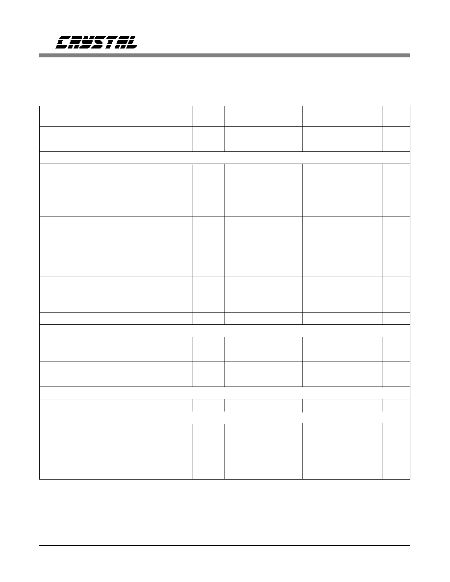
ANALOG CHARACTERISTICS
(T
A
= 25
∞
C for K grade, T
A
= -40 to +85
∞
C for B grade; VA+,VD+
= 5V; VA- = -5V; Logic "1" = VD+; Logic "0" = DGND; Full-Scale Output Sinewave, 991 Hz; Input Word Rate =
48 kHz; Input Data = 18 Bits; BICK = 3.072 MHz; R
L
= 10k
; Measurement Bandwidth is 10 Hz to 20 kHz, un-
weighted; unless otherwise specified.)
Parameter*
CS4328-K
CS4328-B
Symbol
Min
Typ
Max
Min
Typ
Max
Units
Specified Temperature Range
T
A
0
+70
-40
+85
∞
C
Resolution
16
-
-
16
-
-
Bits
Dynamic Performance
Signal-to-Noise Ratio
(A-weighted)
(Note 1)
SNR
120
-
-
120
-
-
dB
Total Harmonic Distortion + Noise (A-Weighted) THD+N
0 dB Output,
-
-93
-90
-
-88
-85
dB
-20 dB Output,
-
-77
-73
-
-75
-70
dB
-60 dB Output,
-
-37
-33
-
-35
-30
dB
Deviation From Linear Phase
(Note 2)
-
-
±
0.5
-
-
±
0.5
-
deg
Passband:
to -3 dB corner
(Notes 3, 4)
-
0
to
23.5
0
to
23.5
kHz
to 0.00025 dB corner
(Notes 3, 4)
0
to
21.6
0
to
21.6
kHz
Frequency Response 10 Hz to 20 kHz (Note 2)
-
-0.05
+0.1
+0.2
-0.05
+0.1
+0.2
dB
Passband Ripple
(Note 4)
-
-
-
0.00025
-
-
0.00025
dB
StopBand
(Note 3)
-
26.4
-
-
26.4
-
-
kHz
StopBand Attenuation
(Note 2)
-
90
-
-
90
-
-
dB
Group Delay (IWR = Input Word Rate)
tgd
-
33/IWR
-
-
33/IWR
-
s
Interchannel Isolation
(1 kHz)
-
-100
-110
-
-95
-105
-
dB
dc Accuracy
Interchannel Gain Mismatch
-
-
0.1
-
-
0.1
-
dB
Gain Error
-
-
-
±
5
-
-
±
5
%
Gain Drift
-
-
150
-
-
150
-
ppm/
∞
C
Offset Error (after calibration)
-
-
-
±
1
-
-
±
1
mV
Analog Output
Full Scale Output Voltage
VOUT
3.8
4.0
4.2
3.8
4.0
4.2
Vpp
Power Supplies
Power Supply Current:
VA+
IA+
-
40
55
-
40
55
mA
VA-
IA-
-
-40
-55
-
-40
-55
mA
VD+
ID+
-
50
60
-
50
60
mA
Power Dissipation
-
-
650
850
-
650
850
mW
Power Supply Rejection Ratio (1 kHz)
PSRR
-
50
-
-
50
-
dB
Notes:
1. Idle channel, digital input all zeros.
2. Combined digital and analog filter characteristics.
3. The passband and stopband edges scale with frequency. For input word rates, IWR, other than
48 kHz, the 0.00025 dB passband edge is 0.45
◊
IWR and the stopband edge is 0.55
◊
IWR.
4. Digital filter characteristics.
CS4328
2
DS62F3
DIGITAL CHARACTERISTICS
(TA = 25
∞
C; VA+ ,VD+ = 5V
±
5%; VA- = -5V
±
5%)
Parameter
Symbol
Min
Typ
Max
Units
High-Level Input Voltage
VIH
70%VD+
-
-
V
Low-Level Input Voltage
VIL
-
-
30%VD+
V
High-Level Output Voltage at Io = -20
µ
A
VOH
4.4
-
-
V
Low-Level Output Voltage at Io = 20
µ
A
VOL
-
-
0.1
V
Input Leakage Current
(Note 5)
Iin
-
-
1.0
µ
A
Note: 5. TST, DIF0 & DIF1 have internal pull-down devices, nominally 90k
.
ABSOLUTE MAXIMUM RATINGS
(AGND1-3, DGND = 0V, all voltages with respect to ground.)
Parameter
Symbol
Min
Max
Units
DC Power Supplies:
Positive Digital
VD+
-0.3
6.0
V
Positive Analog
VA+
-0.3
6.0
V
Negative Analog
VA-
0.3
-6.0
V
|VA+ - VD+|
-
0.4
V
Input Current, Any Pin Except Supplies
Iin
-
±
10
mA
Digital Input Voltage
VIND
-0.3
(VD+)+0.4
V
Ambient Operating Temperature (power applied)
TA
-55
125
∞
C
Storage Temperature
Tstg
-65
150
∞
C
WARNING: Operation at or beyond these limits may result in permanent damage to the device
Normal operation is not guaranteed at these extremes.
RECOMMENDED OPERATING CONDITIONS
(AGND1, AGND2, AGND3, DGND = 0V; all voltages with respect to ground)
Parameter
Symbol
Min
Typ
Max
Units
DC Power Supplies:
Positive Digital
VD+
4.75
5.0
5.25
V
Positive Analog
VA+
4.75
5.0
5.25
V
Negative Analog
VA-
-4.75
-5.0
-5.25
V
|VA+ - VD+|
-
-
0.4
V
CS4328
DS62F3
3

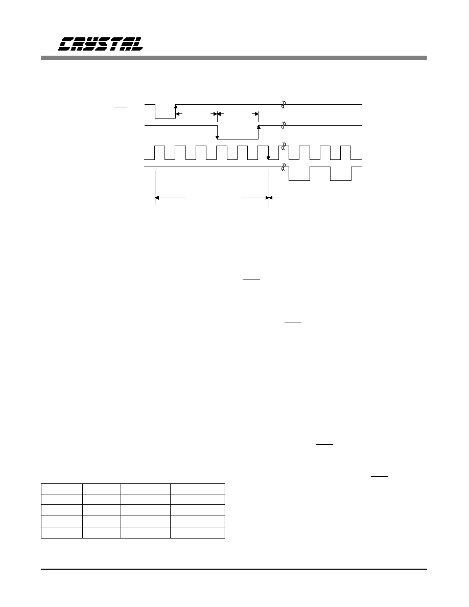
SWITCHING CHARACTERISTICS
(T
A
= 25
∞
C; VA+, VD+ = 5V
±
5%; VA- = -5V
±
5%; Inputs: Logic 0 = 0V, Logic 1 = VD+, C
L
= 20 pF)
Parameter
Symbol
Min
Typ
Max
Units
Master Clock Frequency using Internal Oscillator:
CKS=H
XTI/XTO
10.7
-
19.2
MHz
CKS=L
-
7.1
-
13.9
MHz
Master Clock Frequency using External Clock:
CKS=H
XTI/XTO
0.384
-
19.2
MHz
CKS=L
-
0.256
-
13.9
MHz
XTI/XTO Pulse Width Low
-
21
-
-
ns
XTI/XTO Pulse Width High
-
21
-
-
ns
BICK Pulse Width Low
tbickl
30
-
-
ns
BICK Pulse Width High
tbickh
30
-
-
ns
BICK Period
tbickw
80
-
-
ns
BICK rising to LRCK edge delay
(Note 6)
tblrd
35
-
-
ns
BICK rising to LRCK edge setup time
(Note 6)
tblrs
35
-
-
ns
SDATAI valid to BICK rising setup time
(Note 6)
tsbs
35
-
-
ns
BICK rising to SDATAI hold time
(Note 6)
tbsh
35
-
-
ns
RST Minimum Pulse Width Low
2 periods of XTI/XTO
Note:
6. "BICK rising" refers to modes 0, 1, and 3. For mode 2, replace "BICK rising" with "BICK falling."
bickh
t
blrs
t
blrd
t
sbs
t
bsh
t
bickl
t
SDATAI
BICK
LRCK
bickh
t
blrs
t
blrd
t
sbs
t
bsh
t
bickl
t
SDATAI
BICK
LRCK
MSB
MSB-1
Serial Input Timing (Modes 0, 1, &3)
Serial Input Timing (Mode 2)
CS4328
4
DS62F3

Figure 1. Typical Connection Diagram
CS4328
D/A CONVERTER
CKS
TST
VD+
VA+
AGND1
DGND
11
10
17
25
4
1
16
3
+5V Digital
+5V
Analog
AGND2
AGND3
0.1
µ
F
DIF0
DIF1
13
12
Mode
Select
ACKI
22
ACKO
24
XTI
15
XTO
14
20
LRCK
Audio
Data
Processor
BICK
SDATAI
19
18
0.1
µ
F
7
NC
23
NC
RST
9
Power Up/
Cal. Control
15 pF
1.2 M
10 pF
External Clock
74HC
device
optional crystal oscillator
10
µ
F
+
10
µ
F
+
VA-
0.1
µ
F
5
-5V
Analog
10
µ
F
+
VREF-
28
0.1
µ
F
10
µ
F
+
21
CALO
CALI
27
6
CMPI
8
CMPO
AOUTL
AOUTR
2
26
10 nF
NPO
10 nF
NPO
51
51
0.1
µ
F
CS4328
DS62F3
5

GENERAL DESCRIPTION
The CS4328 is a complete stereo digital-to-ana-
log system designed for digital audio. The
system accepts data at standard audio frequen-
cies, such as 48 kHz, 44.1 kHz, and 32 kHz; and
produces line-level outputs.
The architecture includes an 8
◊
oversampling fil-
ter followed by a 64
◊
oversampled one-bit
delta-sigma modulator. The output from the one
bit modulator controls the polarity of a reference
voltage which is then passed through an ultra-
linear analog low-pass filter. The result is
line-level outputs with no need for further filter-
ing.
SYSTEM DESIGN
Very few external components are required to
support the DAC. Normal power supply decou-
pling components and voltage reference bypass
capacitors are all that's required.
System Clock Input
The master clock (XTI/XTO) input to the DAC
is used to operate the digital interpolation filter
and the delta-sigma modulator. The master clock
can be either a crystal placed across the XTI and
XTO pins, or an external clock input to the XTI
pin with the XTO pin left floating.
The frequency of XTI/XTO is determined by the
desired Input Word Rate, IWR, and the setting of
the Clock Select pin, CKS. IWR is the frequency
at which words for each channel are input to the
DAC and is equal to LRCK frequency. Setting
CKS low selects an XTI/XTO frequency of
256
◊
IWR while setting CKS high selects
384
◊
IWR. The ACKO pin will always be
128
◊
IWR and is used by the analog low-pass
smoothing filter. Table 1 illustrates various audio
word rates and corresponding frequencies used
in the DAC.
The remaining system clocks, LRCK and BICK,
must be synchronously derived from XTI/XTO.
If the CS4328 internal oscillator is used, the cir-
cuit must be configured and XTO buffered as
shown in Figure 1. XTI/XTO can be divided to
produce LRCK and BICK using a synchronous
counter such as 74HC590. Notice that the value
of the capacitor on XTO is 10 pF and the XTI
capacitor is 15 pF, which allows for 5 pF of gate
and stray capacitance.
It is also possible to divide ACKO, 128
◊
IWR,
to derive BICK and LRCK. However, external
circuitry must be used to apply a "kick-start"
pulse to LRCK in order to activate ACKO. The
sequence for the cancellation of RESET, begin-
ning of calibration and activation of ACKO is
shown in Figure 2 with the required transitions
indicated by arrows. A momentary loss of
XTI/XTO or power will require a "kick-start"
pulse to resume operation.
Serial Data Interface
Data is input to the CS4328 via three serial input
pins; SDATAI is the serial data input, BICK is
the serial data clock and LRCK defines the chan-
nel and delineation of data. The DAC supports
four serial data formats which are selected via
the digital input format pins DIF0 and DIF1. The
different formats control the relationship of
LRCK to SDATAI and the edge of BICK used to
LRCK
CKS
XTI/XTO
ACKO
(kHz)
(MHz)
(MHz)
32
low
8.192
4.096
32
high
12.288
4.096
44.1
low
11.2896
5.6448
44.1
high
16.9344
5.6448
48
low
12.288
6.144
48
high
18.432
6.144
Table 1. Common Clock Frequencies
CS4328
6
DS62F3
latch data. Table 2 lists the four formats, along
with the associated figure number. Format 0 is
compatible with existing 16-bit D/A converters
and digital filters. Format 1 is an 18-bit version
of format 0. Format 2 is similar to Crystal ADCs
and many DSP serial ports. Format 3 is compat-
ible with the I
2
S serial data protocol. Formats 2
and 3 support 18-bit input or 16-bit followed by
two zeros. In all four serial input modes, the se-
rial data is MSB-first and 2's-complement
format.
Formats 0, 2 and 3 will operate with 16-bit data
and 16 BICK pulses as well. See Figure 6 for
1 6 - bit t i m i n g . H ow ever, th e use of
BICK = 64
◊
IWR is recommended to minimize
the possibility of performance degradation result-
ing from BICK coupling into VREF-.
Reset and Offset Calibration
RST is an active low signal that resets the digital
filter and the delta-sigma modulator, synchro-
nizes LRCK with internal control signals and
starts an offset calibration cycle upon exiting re-
set. When RST goes low, CALO goes high and
stays high until the end of an offset calibration
cycle. An offset calibration cycle takes 1024
IWR cycles to complete. CALO must be con-
nected to CALI and CMPO must be connected
to CMPI for offset calibration. During an offset
calibration the analog output is forced to zero.
Power-Up Considerations
Upon initial application of power to the DAC,
offset calibration and digital filter registers will
be indeterminate. RST should be low during
power-up to activate an internal mute and pre-
vent this erroneous information from being
output from the DAC. Bringing RST high will
begin a calibration cycle and initialize these reg-
isters.
Muting
There are two types of mutes that can be imple-
mented with the CS4328. The first is a -50 dB
DIF1
DIF0
Mode
Figure
0
0
0
3
0
1
1
3
1
0
2
4
1
1
3
5
Table 2. Digital Input Formats
XTI/XTO
Reset Status
40 ns
minimum
40 ns
minimum
Exit Reset
LRCK
"Kickstart"
ACK0
RST
Figure 2. RESET Cancellation Timing
CS4328
DS62F3
7

LRCK
BICK
Left Channel
Right Channel
SDATAI
6
5
4
3
2
1
0
9
8
7
15 14 13 12 11 10
6
5
4
3
2
1
0
9
8
7
15 14 13 12 11 10
16 Bit
SDATAI
18 Bit
6
5
4
3
2
1
0
9
8
7
15 14 13 12 11 10
17 16
6
5
4
3
2
1
0
9
8
7
15 14 13 12 11 10
17 16
15
17
LRCK
BICK
Left Channel
Right Channel
SDATAI
6 5
4
3
2
1
0
9
8
7
15 14 13 12 11 10
6
5
4
3
2
1 0
9
8
7
15 14 13 12 11 10
16 Bit
SDATAI
18 Bit
6
5
4
3
2
1
0
9
8 7
15 14 13 12 11 10
17 16
6
5
4
3 2
1
0
9
8
7
15 14 13 12 11 10
17 16
Figure 5. Digital Input Format 3
Figure 4. Digital Input Format 2
LRCK
BICK
Left Channel
Right Channel
SDATAI
6
5
4
3
2
1
0
9
8
7
15 14 13 12 11 10
1
0
6
5
4
3
2
1
0
9
8
7
15 14 13 12 11 10
Mode 0
SDATAI
6
5
4
3
2
1
0
9
8
7
15 14 13 12 11 10
1
0
6
5
4
3
2
1
0
9
8
7
15 14 13 12 11 10
Mode 1
17 16
17 16
Figure 3. Digital Input Formats 0 & 1
LRCK
Left Channel
Right Channel
6
5
4
3
2
1
0
9
8
7
15 14 13 12 11 10
6
5
4
3
2
1
0
9
8
7
15 14 13 12 11 10
BICK
BICK
6
5
4
3
2
1
0
9
8
7
15 14 13 12 11 10
6
5
4
3
2
1
0
9
8
7
15 14 13 12 11 10
6
5
4
3
2
1
0
9
8
7
15 14 13 12 11 10
6
5
4
3
2
1
0
9
8
7
15 14 13 12 11 10
SDATAI
Mode 2
SDATAI
Mode 0
SDATAI
Mode 3
*
LRCK must be inverted.
*
Figure 6. Digital Input Formats 0, 2 and 3 with 16 BICK Periods
CS4328
8
DS62F3

mute which can be activated by forcing the
CALI pin high. Figure 7 shows how to imple-
ment a -50 dB mute using an OR gate. The
propagation of the gate will be the only delay in
moving the CS4328 to a muted state.
The second mute option is a two stage operation
which involves forcing SDATAI to 0 using an
AND gate as shown in Figure 8. The first mute
occurs following 33 LRCK cycles when the 0 in-
put data propagates to the output of the DAC.
The rms noise present at the output will typically
be 93 dB below fullscale. Following a total of
4096 LRCK cycles with 0 input data the output
of the CS4328 will mute and lower the output
rms noise to a minimum of 120 dB below
fullscale. Upon release of the MUTE command
and non-zero input data the CS4328 output mute
will immediately release. However, 33 LRCK
cycles are required for input data to propagate to
the output of the CS4328.
Grounding and Power Supply Decoupling
As with any high resolution converter, the
CS4328 requires careful attention to power sup-
ply and grounding arrangements to optimize
performance. Figure 1 shows the recommended
power arrangements with VA+ connected to a
clean +5 volt supply and VA- connected to a
clean -5 volt supply. VD+, which powers the
digital interpolation filter and delta-sigma modu-
lator, may be powered from the system +5 volt
logic supply. Decoupling capacitors should be
located as near to the CS4328 as possible.
The printed circuit board layout should have
separate analog and digital regions with individ-
ual ground planes. The CS4328 should straddle
th e gro un d p lane break as shown on the
CDB4328 Evaluation board. Optional jumpers
for connecting these planes should be included
near the DAC, where power is brought on to the
board and near the regulators. All signals, espe-
cially clocks, should be kept away from the
VREF- pin to avoid unwanted coupling into the
CS4328. The VREF- decoupling capacitors, par-
ticularly the 0.1
µ
F, must be positioned to
minimize the electrical path from VREF- to
Pin 1 AGND and to minimize the path between
VREF- and the capacitors. Extensive use of
ground plane fill on both the analog and digital
sections of the circuit board will yield large re-
ductions in radiated noise effects. An application
note "Layout and Design Rules for Data Con-
verters" is printed in the Application Note
section of this book.
Analog Output and Filtering
Full scale analog output for each channel is typi-
cally 4V peak-to-peak. The analog outputs can
drive load impedances as low as 600
and are
short-circuit protected to 20mA.
The C S4328 an alog filter is a 5th order
switched-capacitor filter followed by a second-
o rd er continuous-time fi lt er. The
switched-capacitor filter is clock dependent and
will scale with the IWR frequency. The continu-
ous-time filter is fixed and not related to IWR. A
low-pass filter consisting of a 51
resistor and a
.01
µ
F NPO capacitor is recommended on the
analog outputs.
21
27
MUTE
CALO
CALI
CS4328
Figure 7. -50dB Muting
18
MUTE
SDATAI
CS4328
DATA
_____
Figure 8. -120 dB Muting
CS4328
DS62F3
9

Performance Plots
The following collection of CS4328 measure-
ment plots (IWR = 48 kHz) were taken with an
Audio Precision Dual Domain System One. All
FFT plots are 16,384 point.
Figure 9 shows the frequency response with a
48 kHz input word rate. The response is very flat
out to half the input word rate.
Figure 10 shows the muted noise with all zeros
data into the CS4328. This plot is dominated by
the noise floor of the System One.
Figure 11 shows the unmuted noise. This data
was taken by feeding the CS4328 continuous ze-
ros, but pulling CALI low. This unmutes the
output stage of the CS4328. This plot shows the
noise shaping characteristics of the delta-sigma
modulator combined with the analog filter.
Figure 12 shows the A-weighted THD+N vs sig-
nal amplitude for a dithered 1kHz input signal.
Notice that there is no increase in distortion as
the signal level decreases. This indicates very
good low-level linearity, one of the key benefits
of the delta-sigma technique.
Figure 13 shows the fade-to-noise linearity test
result using track 20 of the CBS CD-1. The in-
put test signal is a dithered 500 Hz sine wave
which gradually fades from -60 dB level to -120
dB. During the fading, the output level from the
CS4328 is measured and compared to the ideal
level. Notice the very close tracking of the out-
put level to the ideal, even at low level inputs of
-90 dB. The gradual shift of the plot away from
zero at signal levels < -100 dB is caused by the
background noise starting to dominate the meas-
urement.
Figure 14 shows the impulse response, taken
from the single positive full scale value on track
17 of the CD-1 test disk. Notice the high degree
of symmetry, indicating good phase linearity.
Figure 15 shows a 16K FFT plot result, with a
1 kHz -90 dB dithered input. Notice the com-
plete lack of distortion components and tones.
Figure 16 shows a bandlimited, 10 Hz to
22 kHz, time domain plot of the CS4328 output
with a 1 kHz, -90 dB dithered input. Notice the
clear residual sine wave shape, in the presence of
noise.
Figure 17 shows the monotonicity test result
plot. The input data to the CS4328 is +1 LSB, -1
LSB four times, then +2 LSB, -2 LSB four times
and so on, until +10 LSB, -10 LSB. This data
pattern is taken from track 21 of the CD-1 test
disk. Notice the increasing staircase envelope,
with no decreasing elements. Notice also the
clear resolution of the LSB. For this test, one
LSB is a 16-bit LSB.
The following tests were done by filtering the
analog output of the CS4328 with the System
One analyzer 1 kHz notch filter to reduce the
peak signal level. The resulting signal was then
amplified and applied to the DSP module, avoid-
ing distortion in the System One A/D converter.
Figure 18 shows a 16K FFT Plot with a 1 kHz,
0 dB input. Notice the low order harmonic dis-
tortion at < -100 dB.
Figure 19 shows a 16K FFT Plot with a 1 kHz,
-10 dB input. Notice the almost complete ab-
sence of distortion, with a small residual 2nd
harmonic at -110 dB.
CS4328
10
DS62F3

vs
-100
-98
-96
-94
-92
-90
-88
-86
-84
-82
-80
THD+N(dBr)
-100
-90
-80
-70
-60
-50
-40
-30
-20
-10
0
GENAMP(dBFS)
CRYSTAL THDAM18A
Figure 12. THD+N vs 18-bit Input Signal Level
CRYSTAL TR20R
vs
-10
-8
-6
-4
-2
0
2
4
6
8
10
BANDPASS(dBr)
-120
-110
-100
-90
-80
-70
-60
LEVEL(dBr)
Figure 13. Fade-to-Noise Linearity
CRYSTAL IMPULSE
vs
-0.500
-0.083
0.333
0.750
1.167
1.583
2.000
AMP1(V)
0.0
95.8
192
287
383
479
575
670
766
862
TIME(usec)
Figure 14. Impulse Response
CRYSTAL FRQRSP48
vs
-2.0
-1.5
-1.0
-0.5
0.0
0.5
1.0
1.5
2.0
AMPL(dBr)
10
100
1k
10k
30k
GENFRQ(Hz)
Figure 9. Frequency Response (48 kHz word rate)
CRYSTAL NOISE
&
vs
-160
-140
-120
-100
-80
-60
-40
-20
0
AMP1(dBr)
AMP1(dBr)
0.02
9.82
19.6
29.4
39.2
49.0
58.8
68.6
78.4
88.2
98.0
FREQ(kHz)
Figure 10. Muted Idle Channel Noise
CRYSTAL NOISEUNM
vs
-160
-140
-120
-100
-80
-60
-40
-20
0
AMP1(dBr)
0.02 9.82
19.6
29.4
39.2
49.0
58.8
68.6
78.4
88.2
98.0
FREQ(kHz)
Figure 11. Unmuted Idle Noise
CS4328
DS62F3
11

CRYSTAL 1k 0dBFFT
vs
-140
-120
-100
-80
-60
-40
-20
0
AMP1(dBr)
20
100
1k
10k
20k
FREQ(Hz)
Figure 18. 1 kHz, 0 dB Input FFT Plot
CRYSTAL 1KM10DB
vs
-140
-120
-100
-80
-60
-40
-20
0
AMP1(dBr)
20
100
1k
10k
20k
FREQ(Hz)
Figure 19. 1 kHz, -10 dB Input FFT Plot
CRYSTAL M90DB1K
vs
-140
-120
-100
-80
-60
-40
-20
0
AMP1(dBr)
20
100
1k
10k
20k
FREQ(kHz)
Figure 15. 1 kHz, -90 dB Input FFT Plot
CRYSTAL M90TIME
vs
-250
-200
-150
-100
-50
0
50
100
150
200
250
AMP1(uV)
0.0
0.50
1.00
1.50
2.00
2.50
3.00
TIME(msec)
Figure 16. 1 kHz, -90 dB Input Time Domain Plot
CRYSTAL MONOTON
vs
-800
-640
-480
-320
-160
0
160
320
480
640
800
AMP1(uV)
0
5
10
15
20
25
30
35
40
45
50
TIME(msec)
Figure 17. Monotonicity Test (16-bit data)
CS4328
12
DS62F3

THEORY OF OPERATION
The CS4328 architecture can be considered in
five blocks: Interpolation, sample/hold, delta-
sigma modulation, D/A conversion, and analog
filtering.
Audio data is input to the CS4328 digital inter-
polation filter which removes images of the input
signal that are present at multiples of the input
sample frequency, Fs (Figure 21). Following the
interpolation stage, the resulting frequency spec-
trum has images of the input signal at multiples
of eight times the input sample frequency, 8
◊
Fs
(Figure 22). Eliminating the images between Fs
and 8
◊
Fs greatly relaxes the requirements of the
analog filtering, allowing the suppression of im-
ages while leaving the audio band of interest
unaltered.
The CS4328 interpolation stage is followed by a
sample-and-hold function where the data points
from the interpolator are held for eight (64
◊
Fs)
clock cycles. The resulting frequency response
is a sinx/x characteristic with zeros at 8
◊
Fs mul-
tiples. The sinx/x zeros completely attenuate
signals at 8
◊
Fs and largely suppress the remain-
ing energy of the images (Figure 23). The 8
◊
interpolation followed by the 8
◊
sample-and-
hold results in data at a rate of 64
◊
Fs.
The delta-sigma modulator takes in the 64
◊
Fs
data (3.072 MHz for 48kHz sampled systems)
and performs fifth-order noise shaping. In the
digital modulator of the CS4328, 18-bit audio
data is modulated to a 1-bit, 64
◊
Fs signal. The
5th-order noise shaper allows 1-bit quantization
to support 18-bit audio processing by suppress-
ing quantization noise in the bandwidth of
interest. Figure 24 shows the frequency spec-
trum of the modulator output.
The CS4328's digital modulator is followed by a
D-to-A converter that translates the 1-bit signal
into a series of charge packets. The magnitude
of the charge in each packet is determined by
sampling of a voltage reference onto a switched
Audio
Data
Analog
Output
Continuous
Time
Filter
DAC
8 X S/H
8x
Interpolator
Delta
Sigma
Modulator
Digital
Switched
Cap
LPF
Analog Filter
Figure 20. CS4328 Architecture
f (kHz)
8Fs
16Fs
24
(dB)
Figure 23. Spectrum After S/H
f (kHz)
8Fs
16Fs
24
(dB)
Figure 22. 8X Interpolated Data Spectrum
f(kHz)
24
(dB)
Figure 24. Modulator Output Spectrum
f (kHz)
Fs
2Fs
24
(dB)
Figure 21. Input Data Spectrum
CS4328
DS62F3
13
capacitor, where the polarity of each packet is
controlled by the 1-bit signal. The result is a
1-bit D/A conversion process that is very insensi-
tive to clock jitter. This is a major improvement
over previous generations of 1-Bit D/A convert-
ers where the magnitude of charge in the D/A
process is determined by switching a current ref-
erence for a period of time defined by periods of
the master clock.
The final stage of the CS4328 is made up of a
5th order switched-capacitor low pass filter and a
2nd order continuous time filter. The switched-
capacitor filter eliminates out-of-band energy re-
s u l t i n g f r o m t h e n o i se sh ap i n g p r o ces s
(Figure 25). The switched-capacitor stage scales
with the master clock signal being applied to the
CS4328. The final stage is a 2nd order continu-
ous time filter that eliminates high frequency
energy that appears at multiples of the 64
◊
Fs
sample rate (Figure 26).
Figures 27-30 are computer simulations of the
combined response of the CS4328 digital and
analog filters with an input word rate of 48 kHz.
Figure 27 shows the individual and combined
phase response of the CS4328 filters. Notice the
digital filter equalization of the analog filter to
produce a linear phase response.
Figures 28-30 are plots of the CS4328 magni-
tude response.
0
2
4
6
8
10
12
14
16
18
20
Frequency (kHz)
-20
-16
-12
-8
-4
0
4
8
12
16
20
P
h
ase (degre
es)
Analog Filter
Digital Filter
Total Phase
Figure 27. Deviation From Linear Phase
f (kHz)
24
64Fs
(dB)
Figure 25. Spectrum After Switched-Capacitor Filter
f (kHz)
24
(dB)
Figure 26. Spectrum After Continuous Time Filter
CS4328
14
DS62F3

20
21
22
23
24
25
Input Frequency (kHz)
-10
-9
-8
-7
-6
-5
-4
-3
-2
-1
0
1
M
agn
i
t
ud
e (
d
B
)
Figure 29. Combined Digital and Analog
Filter Frequency Response
22
23
24
25
26
27
28
29
30
Input Frequency (kHz)
-110
-100
-90
-80
-70
-60
-50
-40
-30
-20
-10
0
M
agn
i
t
ud
e (
d
B
)
Figure 30. Combined Digital and Analog
Filter Transition Band
0
8
16
24
32
40
48
Input Frequency (kHz)
-130
-120
-110
-100
-90
-80
-70
-60
-50
-40
-30
-20
-10
0
10
M
agn
i
t
ud
e (
d
B
)
Figure 28. Combined Digital and Analog
Filter Frequency Response
CS4328
DS62F3
15

PIN DESCRIPTIONS
Power Supply Connections
VA+ - Positive Analog Power, PIN 3.
Positive analog supply. Nominally +5 volts.
VA- - Negative Analog Power, PIN 5.
Negative analog supply. Nominally -5 volts.
AGND1, AGND2, AGND3 - Analog Grounds, PINS 1, 4, 25.
Analog ground reference.
VD+ - Positive Digital Power, PIN 16.
Positive supply for the digital section. Nominally +5 volts.
DGND - Digital Ground, PIN 17.
Digital ground for the digital section.
Analog Outputs
VREF- - Voltage Reference Output, PIN 28.
Nominally -3.68 volts. Normally connected to a 0.1
µ
F ceramic capacitor in parallel with a
10
µ
F or larger electrolytic capacitor. Note the negative output polarity.
AOUTL - Analog Left Channel Output, PIN 2.
Analog output for the left channel. Typically 4V peak-to-peak for a full-scale input signal.
AOUTR - Analog Right Channel Output, PIN 26.
Analog output for the right channel. Typically 4V peak-to-peak for a full-scale input signal.
ANALOG GROUND AGND1
VREF-
VOLTAGE REFERENCE OUTPUT
ANALOG LEFT CHANNEL OUTPUT AOUTL
CALI
CALIBRATION INPUT
ANALOG POWER
VA+
AOUTR ANALOG RIGHT CHANNEL OUTPUT
ANALOG GROUND AGND2
AGND3 ANALOG GROUND
NEGATIVE ANALOG POWER
VA-
ACKI
ANALOG CLOCK INPUT
COMPARATOR OUTPUT
CMPO
NC
NO CONNECT
NO CONNECT
NC
ACKO
ANALOG CLOCK OUTPUT
COMPARATOR INPUT
CMPI
CALO
CALIBRATION OUTPUT
RESET
RST
LRCK
LEFT/RIGHT CLOCK INPUT
TEST
TST
BICK
SERIAL BIT CLOCK INPUT
CLOCK SELECT
CKS
SDATAI SERIAL DATA INPUT
DIGITAL INPUT FORMAT 1
DIF1
DGND
DIGITAL GROUND
DIGITAL INPUT FORMAT 0
DIF0
VD+
DIGITAL POWER
CRYSTAL OR CLOCK INPUT
XTI
XTO
CRYSTAL OSCILLATOR OUTPUT
1
2
3
4
5
6
7
8
9
10
11
12
13
14
28
27
26
25
24
23
22
21
20
19
18
17
16
15
CS4328
16
DS62F3

Digital Inputs
XTI - Crystal or Clock Input, PIN 14.
A crystal oscillator can be connected between this pin and XTO, or an external CMOS clock
can be input on XTI. The frequency must be either 256
◊
or 384
◊
the input word rate based on
the clock select pin, CKS.
ACKI - Analog Clock Input, PIN 24.
This is the master clock input for the analog section of the chip and must be 128
◊
the input
word rate. ACKI is typically connected to the Analog Clock Ouput pin, ACKO.
CALI - Calibration Input, PIN 27.
Input to the analog section that is used during offset calibration. Normally connected to the
Calibration Output pin, CALO.
CMPI - Comparator Input, PIN 8
Input to the digital section that is used during offset calibration. Normally connected to the
Comparator Output pin, CMPO.
LRCK - Left/Right Clock, PIN 20.
This input determines which channel is currently being input on the Serial Data Input pin,
SDATAI. The format of LRCK is controlled by DIF0 and DIF1.
BICK - Serial Bit Input Clock, PIN19.
Clocks the individual bits of the serial data in from the SDATAI pin. The edge used to latch
SDATAI is controlled by DIF0 and DIF1.
SDATAI - Serial Data Input, PIN 18.
Two's complement MSB-first serial data of either 16 or 18 bits is input on this pin. The data is
clocked into the CS4328 via the BICK clock and the channel is determined by the LRCK clock.
The format for the previous two clocks is determined by the Digital Input Format pins, DIF0
and DIF1
DIF0,DIF1 - Digital Input Format, PINS 13, 12
These two pins select one of four formats for the incoming serial data stream. These pins set
the format of the BICK and LRCK clocks with respect to SDATAI. The formats are listed in
Table 2.
CKS - Clock Speed Select, PIN 11.
Selects the clock frequency input on the XTI pin. CKS low selects 256
◊
the input word rate
(LRCK frequency) while CKS high selects 384
◊
.
RST - Reset and Calibrate, PIN 9.
When reset is low the filters and modulators are held in reset. When reset goes high, an offset
calibration is initiated.
CS4328
DS62F3
17

Digital Outputs
XTO - Crystal Oscillator Output, PIN 15.
When a crystal oscillator is used, it is tied between this pin and XTI. When an external clock is
input, this pin should be left floating.
ACKO - Analog Clock Output, PIN 22.
This output is 128
◊
the input word rate (LRCK frequency). Normally connected to the Analog
Clock Input pin, ACKI.
CALO - Calibration Output, PIN 21.
Used during offset calibration. Must be connected to the Calibration Input pin, CALI.
CMPO - Comparator Output, PIN 6.
Used during offset calibration. Must be connected to the Comparator Input pin, CMPI.
Miscellaneous
NC - No Connection, PINS 7, 23.
These two pins are bonded out to test outputs. They must not be connected to any external
component or any length of PC trace.
TST -Test Input, PIN 10.
Allows access to the CS4328 test modes, which are reserved for factory use. Must be tied to
DGND.
CS4328
18
DS62F3

PARAMETER DEFINITIONS
Total Harmonic Distortion + Noise - The ratio of the rms value of the signal to the rms sum of all
other spectral components over the specified bandwidth (typically 10 Hz to 20 kHz), including
distortion components. Expressed in decibels.
Signal-to-Noise Ratio - The ratio of the full scale rms value of the signal to the rms sum of all other
spectral components over the specified bandwidth with an input of all zeros.
Frequency Response - A measure of the amplitude response variation from 10 Hz to 20 kHz relative
to the amplitude response at 1 kHz. Units in decibels.
Interchannel Isolation - A measure of crosstalk between the left and right channels. Measured for
each channel at the converter's output with all zeros to the input under test and a full-scale
signal applied to the other channel. Units in decibels.
Interchannel Gain Mismatch - The gain difference between left and right channels. Units in decibels.
Gain Error - The deviation from the nominal full scale analog output for a full scale digital input.
Gain Drift - The change in gain value with temperature. Units in ppm/
∞
C.
Offset Error - The deviation of the mid-scale transition (111...111 to 000...000) from the ideal
(AGND). Units in mV.
CS4328
DS62F3
19

28 pin
Plastic DIP
1
28
15
14
MILLIMETERS
INCHES
DIM
MIN
MAX
MIN
MAX
D
B
A
L
C
13.72
14.22 0.540
0.560
36.45
1.02
0.36
0.51
3.94
3.18
0.20
0∞
15.24
37.21
1.65
0.56
1.02
5.08
3.81
0.38
15∞
1.435
0.040
0.014
0.020
0.155
0.125
0.600
0.008
0∞
1.465
0.065
0.022
0.040
0.200
0.150
0.015
15∞
15.87
0.625
2.41
2.67 0.095
0.105
C
eA
E1
D
B
SEATING
PLANE
A
B1
e1
A1
L
NOTES:
1. POSITIONAL TOLERANCE OF LEADS SHALL BE WITHIN
0.25mm (0.010") AT MAXIMUM MATERIAL CONDITION, IN
RELATION TO SEATING PLANE AND EACH OTHER.
2. DIMENSION eA TO CENTER OF LEADS WHEN FORMED PARALLEL.
3. DIMENSION E1 DOES NOT INCLUDE MOLD FLASH.
NOM
13.97
36.83
1.27
0.46
0.76
4.32
-
0.25
-
-
2.54
NOM
0.550
1.450
0.050
0.018
0.030
0.170
-
-
0.010
-
0.100
A1
B1
E1
e1
eA
SOIC
MILLIMETERS
INCHES
MIN
MAX
MAX
MIN
0.095
0.105
2.41
2.67
0.008
0.015
0.203
0.381
0.398
0.420
10.11
10.67
0.020
0.013
0.51
0.33
0.016
0.035
0.41
0.89
8∞
0∞
0∞
8∞
MILLIMETERS
INCHES
MIN
MAX
MAX
MIN
pins
0.410
0.390
9.91
10.41
16
0.510
0.490
12.45
12.95
20
0.610
0.590
14.99
15.50
24
0.710
0.690
17.53
18.03
28
0.012
0.005
0.127
0.300
1.14
0.040
DIM
E
E
b
L
D
e
A
A
c
0.292
0.298
7.42
7.57
D
E
E1
e
A
A
b
1
A2
c
L
µ
1
µ
1
1.40
0.055
A 2
see table above
NOM
2.54
0.280
10.41
0.46
-
-
NOM
10.16
12.70
15.24
17.78
-
7.49
1.27
2.29
2.54
2.41
NOM
0.100
0.011
0.410
0.018
-
-
NOM
0.400
0.500
0.600
0.700
-
0.295
0.050
0.100
0.090 0.095

Features
∑
Demonstrates recommended layout
and grounding arrangements
∑
CS4328 Supports multiple input formats
∑
CS8412 Receives AES/EBU, S/PDIF,
& EIAJ-340 Compatible Digital Audio
∑
Digital and Analog Patch Areas
∑
Operation with on-board CS8412 or
externally supplied system timing
General Description
The CDB4328 evaluation board allows fast evaluation
of the CS4328 18-bit, stereo D/A converter. The board
provides an analog output interface via BNC connec-
tors for both channels. Evaluation requires an analog
signal analyzer, a digital signal source, and a power
supply.
Also included is a CS8412 digital audio receiver I.C.,
which will accept AES/EBU, S/PDIF, and EIAJ-340
compatible audio data. The CS8412 can provide the
system timing necessary to operate the CS4328.
The evaluation board may also be configured to accept
external timing signals for operation in a user applica-
tion during system development.
ORDERING INFORMATION: CDB4328
Crystal Semiconductor Corporation
P.O. Box 17847, Austin, TX 78760
(512) 445 7222 Fax: (512) 445 7581
http://www.crystal.com
AUG '93
DS62DB2
21
CS4328 Evaluation Board
CDB4328
Error Info/
Channel
Status
-15V GND
+15V
GND
+5V
L/R SCLK SDATA MCLK
Power Supply
Regulation and Conditioning
AOUTR
AOUTL
Analog
Patch
Area
Digital
Patch
Area
CS4328
D/A Converter
Offset
Calibration
Network
Digital Audio Input
Timing
Signal
Selector
CS8412
Digital
Audio
Receiver
6
Block Diagram

Power Supply Circuitry
Figure 1 shows the evaluation board power sup-
ply circuitry. Power is supplied to the evaluation
board by five binding posts. The +5 V analog
power supply inputs of the converter are derived
from + 15 V using the voltage regulators U5 and
U6. The +5 V digital supply for the converter
and the discrete logic on the board is provided
by the +5 V and DGND binding posts. D1, D2,
and D3 are transient suppressors which also pro-
vide protection from incorrectly connected
power supply leads. C1-C8 provide general
power supply filtering for the analog supplies.
As shown in Figure 2, C20-C24 provide local-
ized decoupling for the converter VA+ and VA-
pins. Note that C22 is connected between VA-
and VA+ and not VA- and AGND. The evalu-
ation board uses both an analog and a digital
ground plane which are connected at J1. This
ground plane arrangement isolates the board's
digital logic from the analog circuitry.
Offset Calibration & Reset Circuitry
Figure 1, shows the offset calibration circuit pro-
vided on the evaluation board. Upon power-up,
this circuit provides a pulse on the Digital to
Analog Converter's RST pin initiating an offset
calibration cycle. Pressing and releasing S2 also
initiates an offset calibration cycle.
Serial Data Interface
Figure 1 shows that there are two options for in-
puting serial data into the CS4328. Serial data
can be provided via the SDATA BNC connector
on the evaluation board. BNC connectors for
SCLK, the serial data input clock, and L/R, the
clock that defines the channel and delineates the
data, are also provided on the evaluation board.
This information can also be provided by the on-
board CS8412. JP3 selects the source of
SDATA, SCLK, and L/R that will be provided to
the converter. JP3 selections are shown in Ta-
ble 1.
C6
C7
C5
C8
0.22 uF
0.47 uF
J1
+ C3
47 uF
C4
+
47 uF
0.22 uF
OUT
COM
U5
78L05
IN
D3
D2
0.47 uF
C2
+ C1
47 uF
0.1 uF
D1
+15V
-15V
+5V
79L05
U6
COM
IN
OUT
DGND
AGND
VA+
VA-
VD+
D1 = P6KE-6V8P from Thomson
D2 = D3 = 1N6276A 1.5KE
AGND
DGND
VD+
10k
C15
0.1uF
D13
1N148
S2
CAL
R4
4
3
U7B
74HC14
6
5
U7C
RST
CS4328
Figure 1. Power Supply and Reset Circuitry
CDB4328
22
DS62DB2

The CS4328 supports four serial data input for-
mats. The selection of which is made via the
digital input format pins DIF0 and DIF1. The
different formats control the relationship of L/R
to SDATA and the edge of SCLK used to latch
the data. Consult the CS4328 data sheet for an
explanation of the different formats.
System Timing
The master clock input to the CS4328 can be
provided by several sources. JP3 selects the
source of the master clock that is to be supplied
to the XTI pin of the converter. When EXT
CLK is selected, the master clock is provided by
one of two sources. The 12.288 MHz clock sig-
nal provided by U8 can be used as the master
clock for both the CS4328 and the external sys-
tem that provides the serial data to the board.
The other option is for a master clock that is
synchronized to the external serial data coming
into the board, be used as the master clock for
the CS4328 as well. However, if an external
NC
NC
LRCK
BICK
SDATAI
XTI
XTO
RST
CKS
DIFO
DIFI
VREF
AOUTR
AOUTL
CALI
CALO
CMPI
CMPO
AGND3
AGND2
AGND1
VA+
ACKI
ACKO
VD+
VD+
11
13
VD+
12
R11
47k
10
17
TST DGND
28
26
C19
10 nF NPO
C16
0.1 uF
C17
10 uF
51
R6
2
C18
10 nF NPO
51
R5
VA-
-5V Analog,
VA-
+5V Analog,
VA+
+
C24
1.0 uF
C23
0.1 uF
C22
0.1 uF
AOUTL
AOUTR
VD+
1 uF
C26
0.1 uF
C25
U3, Pin 3
U3, Pin 6
U3, Pin 8
U3, Pin 11
L/R SCLK SDATA MCLK
15
14
18
19
20
7
23
9
From
Reset
Circuit
+
16
22
24
1
5
4
25
6
8
21
27
3
U1
CS4328
C20
1.0 uF
C21
0.1 uF
TP
TP
TP
TP
+
+
TP
TP
JP2
Figure 2. CS4328 DAC Connections
Position
Input Option Selected
EXT CLK
SDATA,SCLK, L/R provided
by an external source.
8412
SDATA,SCLK, L/R provided
by the CS8412
Table 1. JP3 Selectable Options
CDB4328
DS62DB2
23

master clock is to be used, U8 must be removed
from it's socket to prevent the two clock signals
from interfering with one another. When 8412 is
selected by JP3, the master clock for the CS4328
is provided by the MCK output of the CS8412.
The CKS pin of the CS4328 can be pulled either
high or low via JP2. This determines whether
the master clock frequency has to be 384X or
256X the input word rate. Consult the CS4328
data sheet for the common master clock frequen-
cies table.
Analog Outputs
The analog outputs are available at 2 BNC con-
nectors labeled AOUTL and AOUTR. R5 and
C18 remove the remaining very high frequency
components from the left channel output signal
while R6 and C19 do so for the right channel
output signal.
Digital Audio Standard Interface
Included on the evaluation board is a CS8412
Digital Audio Interface Receiver. This device
can receive and decode data according to the
AES/EBU, S/PDIF, and EIAJ-340 interface
standard. Figure 3 shows the schematic for the
CS8412. The input is coupled to the device
through a transformer that is included on the
board. The input to the device can be configured
to accept either professional or consumer input
modes. Consult the CS8412 data sheet for an
explanation of the two input modes.
The LEDs, D4-D8, perform two functions.
When S1 is in the Channel Status position, the
LEDs display the channel status information for
the channel selected by JP1. When S1 is in the
Error Information position, the LEDs D4-D6,
display encoded error information that can be
decoded by consulting the CS8412 data sheet.
Encoded sample frequency information is dis-
played on LEDs D7-D9 provided a proper clock
is being applied to the FCK pin of JP1. When
an LED is lit, this indicates a "1" on the corre-
sponding pin located on the CS8412. When an
LED is off, this indicates a "0" on the corre-
sponding pin. Neither the L or R option should
be selected if the FCK pin of JP1 is being driven
by a clock signal.
Serial Output Interface
The SDATA, SCLK, L/R, and MCLK BNC
connectors can also be used to provide a serial
output interface for the CS8412. With JP3 in the
8412 position, the outputs from the CS8412 can
be brought off the board to an external evalution
system. This data can be configured in one of
seven selectable formats. These formats are out-
lined in the CS8412 data sheet.
CDB5336/7/8/9 Interface to CDB4328
Many users find it informative to evaluate a
combined ADC and DAC system connected to-
gether yielding analog input and analog output.
This can be accomplished by interconnecting a
C D B 5 3 2 6 /7 / 8 /9 o r C D B5 3 3 6 / 7 /8 / 9 to a
CDB4328 evaluation board. The following in-
formatio n con tains several tech niques to
accomplish this goal. There are two general
points which need to be mentioned. An analog
input of
±
3.68 V will produce a full scale digital
o ut p u t f r o m t h e C S 5 3 3 6 / 7 / 8 / 9 a n d th e
CS5326/7/8/9. A full scale digital input to the
CS4328 will produce a full scale output of
±
2 V
resulting in an overall loss of approximately
5.2 dB from input to output. Also it is recom-
mended that the power connections for each
board are brought directly from the power sup-
ply and not in a "daisy-chain" manner from
board to board.
Connecting the CDB4328 to the CDB5336/7/8/9
can be accomplished using one of two methods:
CDB4328
24
DS62DB2

7
DG
N
D
M0
M1
M2
M3
23
24
18
17
VD
+
FIL
T
R1
0
C
1
2
20
VD+
V
A+
0.
1 u
F
C1
1
72
2
R9
10
+5
V An
a
l
o
g
1
.
0 uF
C9
+
0.
1 u
F
C1
0
MC
K
SD
A
T
A
SC
K
F
SYN
C
47 k
R2
2
3
1
P
i
n 20,
U1
47 k
R1
56
P
i
n 19,
U1
47 k
R1
3
98
P
i
n 18,
U1
R1
2
12
11
14
VD
+
C2
9
0
.1
u
F
4
10
13
74H
C
1
26
U3
11
12
26
19
1
3
5
7
2
4
6
8
JP
3
VD+
1
2
.2
8
8
M
H
z
GN
D
VCC
NC
U6
C1
3
0
.
1 uF
C1
4
1.
0 uF
+
14
1
8
7
R3
47
k
P
i
n 14,
U1
SE
L
C
hanne
l
S
t
a
t
u
s
S1
VD
+
E
r
r
o
r In
fo
rm
a
t
i
o
n
U7
A
21
T
P
TP
TP
T
P
VE
RF
U
C
ERF
28
14
1
16
25
8
AG
ND
21
1:
1
Di
g
i
t
a
l
In
p
u
t
1
2
3
4
11
0
R8
S
c
h
o
t
t
67
12
54
5
0
P
u
lse
PE
6
5612
C
0
/E0
C
a
/E1
C
b
/E2
Cc
/
F
0
Cd
/
F
1
Ce
/
F
2
CS
L
R
/
F
CK
RX
P
RX
N
VD
+
R7
L
R
FC
K
47
k
TP
CB
L
15
9
10
13
89
10
1
1
12
1
3
VD
+
VD+
0
.
1 uF
C2
8
U7
D,E
,
F
14
7
U2
C
S
8
412
84
12
EX
T
CL
K
JP
1
47 k
1k
0.
04
7
uF
D4
89
56
0
D5
65
56
0
D6
10
11
56
0
D7
43
56
0
D8
12
13
56
0
D9
21
56
0
VD+
7 Pi
n SIP
RP1
VD+
C2
7
0.1
uF
7
6
5
4
3
2
27
U4
74
H
C
0
4
F
i
gu
r
e
3.
CS
84
12
Di
gi
t
a
l
Au
d
i
o Rec
e
i
v
er
Co
n
n
e
c
t
i
o
n
s
CDB4328
DS62DB2
25

the trace at the SDATA BNC connector and
place a jumper between the SDATA BNC and
U8 pin 11. CMODE is set LOW for a master
clock of 256 times the sample rate. P7 must
have both the internal and external jumpers in-
stalled. This will route the master clock to the
E XT C LK IN B NC fo r co nn ec tion to the
CDB4328 MCLK.
If a CS5336/8 is installed an additional modifi-
cation is required to invert the SCLK prior to
transmission to the CDB4328. This can be im-
plemented as follows: cut the trace at the SCLK
BNC and install a jumper between U7 pin 4 and
the SCLK BNC.
CDB5336/7/8/9 and CDB4328 Interconnection
for Method 2
Shielded coaxial cables with BNC connectors
should be used to make the following connec-
tions: L/R to L/R, SCLK to SCLK, SDATA to
SDATA, EXTCKIN to MCLK.
CDB4328 Interfacing to the CDB5326/7/8/9
A method of interfacing the CDB5326/7/8/9 and
the CDB4328 requires a direct interface through
the EXTCLKIN, SCLK, SDATA, and L/R BNC
connectors. This technique requires modifica-
tions to the CDB5326/7/8/9 to derive the proper
clock frequencies. This is done by utilizing a
12.288 MHz clock and supplying a clock to the
CDB5326/7/8/9 at 6.144 MHz.
CDB4328 Configuration
The CS4328 must be set to receive data in for-
mat 2 (DIF1 high and DIF0 low). Modify the
jumpers located near pins 12 and 13 of the
CS4328. JP2 sets the clock to sample frequency
ratio (CKS) on the CS4328 and is set low for a
256 ratio.
JP3 selects the source of SDATA, SCLK and L/R
that will be provided to the converter and should
be removed to access the multiple clocks from
the CDB5326/7/8/9. Remove the 12.288 MHz
oscillator (U8).
CDB5326/7/8/9 Configuration
Remove the clock source jumper (P2). Remove
the 6.144 MHz oscillator (U2) and replace with
the 12.288 MHz oscillator from the CDB4328.
Install a divide by 2 functi on on the
CDB5326/7/8/9 digital patch area. Use a
74HC74 with the D input connected to the Q
output. Connect the oscillator output to the
74HC74 clock input. Connect the Q output to
U1 pin 23.
Position P2 to connect the oscillator output to
the EXTCLKIN.
CDB5326/7/8/9 and CDB4328 Interconnection
Shielded coaxial cables with BNC connectors
should be used to make the following connec-
tions: L/R to L/R, SCLK to SCLK, SDATA to
SDATA, EXTCLKIN to MCLK.
CDB4328
DS62DB2
27

Figure 4. Top Ground Plane Layer (NOT TO SCALE)
CDB4328
28
DS62DB2

Figure 5. Bottom Trace Layer (NOT TO SCALE)
CDB4328
DS62DB2
29

Figure 5. Silk Screen Layer (NOT TO SCALE)
CDB4328
30
DS62DB2

∑ Notes ∑

Smart
Analog
TM
is a Trademark of Crystal Semiconductor Corporation