| –≠–ª–µ–∫—Ç—Ä–æ–Ω–Ω—ã–π –∫–æ–º–ø–æ–Ω–µ–Ω—Ç: CS4360-BS | –°–∫–∞—á–∞—Ç—å:  PDF PDF  ZIP ZIP |

Preliminary Product Information
This document contains information for a new product.
Cirrus Logic reserves the right to modify this product without notice.
1
Copyright
©
Cirrus Logic, Inc. 2001
(All Rights Reserved)
P.O. Box 17847, Austin, Texas 78760
(512) 445 7222 FAX: (512) 445 7581
http://www.cirrus.com
CS4360
24-Bit, 192 kHz 6 Channel D/A Converter
Features
l
24-Bit Conversion
l
102 dB Dynamic Range
l
-90 dB THD+N
l
+3 V to +5 V Power Supply
l
Digital Volume Control with Soft Ramp
≠ 119 dB Attenuation
≠ 1 dB Step Size
≠ Zero Crossing Click-Free Transitions
l
Low Power Consumption
≠ 105 mW with 3 V supply
l
ATAPI Mixing
l
Low Clock Jitter Sensitivity
l
Popguard Technology
Æ
for Control of Clicks
and Pops
Description
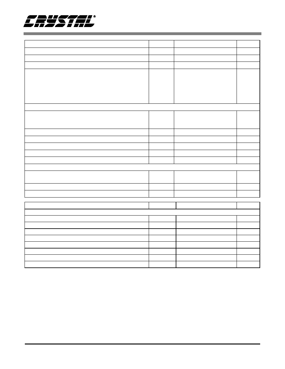
The CS4360 is a complete 6-channel digital-to-analog
system including digital interpolation, fourth-order delta-
sigma digital-to-analog conversion, digital de-emphasis,
volume control, channel mixing and analog filtering. The
advantages of this architecture include: ideal differential
linearity, no distortion mechanisms due to resistor
matching errors, no linearity drift over time and tempera-
ture and a high tolerance to clock jitter.
The CS4360 accepts data at audio sample rates from
4 kHz to 200 kHz, consumes very little power and oper-
ates over a wide power supply range. These features are
ideal for cost-sensitive, multi-channel audio systems in-
cluding DVD players, A/V receivers, set-top boxes,
digital TVs and VCRs, mini-component systems, and
mixing consoles.
ORDERING INFORMATION
CS4360-KS
-10 to 70 ∞C
28-pin SOIC
CS4360-BS
-40 to 85 ∞C
28-pin SOIC
CS4360-KZ
-10 to 70 ∞C
28-pin TSSOP
CS4360-BZ
-40 to 85 ∞C
28-pin TSSOP
CDB4360
Evaluation Board
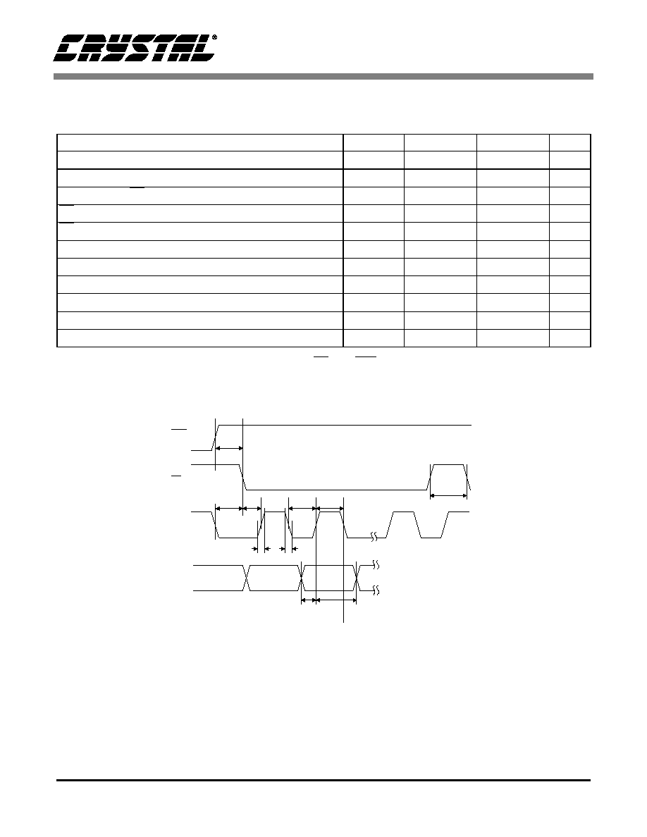
I
C o nt r o l P o rt
E xt e rn a l
M ut e C o nt r ol
R S T
V ol u m e C o nt r o l
I nt e r p o lat i o n F i lt e r
A n alo g F i lt e r
A O U T A1
D A C
Mi x e r
V ol u m e C o nt r o l
D A C
A n alo g F i lt e r
A O UT B1
I nt er p o lat i o n F i lt e r
V ol u m e C o nt r o l
I nt e r p o la ti o n F i lt e r
A n alo g Fi lt e r
A O U T A2
D A C
Mi x e r
V ol u m e C o nt r o l
D A C
A n alo g F i lt e r
A O UT B2
I nt er p o lat i o n F i lt e r
V ol u m e C o nt r o l
I nt e r p o la ti o n F i lt e r
A n alo g Fi lt e r
A O U T A3
D A C
Mi x e r
V ol u m e C o nt r o l
D A C
A n alo g F i lt e r
A O UT B3
I nt er p o lat i o n F i lt e r
M C L K
Se
r
i
a
l
P
o
r
t
L R C K
S C L K
S D I N 1
S D I N 2
S D I N 3
DIF1/SCL/CCLK DIF0/SDA/CDIN M1/AD0/CS
VLC
˜
2
VQ
FILT+
VA
GND
VD
VLS
MUTEC1
MUTEC2
MUTEC3
M2
GND
FEB `01
DS517PP1

CS4360
2
DS517PP1
TABLE OF CONTENTS
1. CHARACTERISTICS AND SPECIFICATIONS ......................................................................... 5
ANALOG CHARACTERISTICS ................................................................................................ 5
POWER AND THERMAL CHARACTERISTICS....................................................................... 7
DIGITAL CHARACTERISTICS ................................................................................................. 7
ABSOLUTE MAXIMUM RATINGS ........................................................................................... 7
RECOMMENDED OPERATING CONDITIONS ....................................................................... 8
SWITCHING CHARACTERISTICS .......................................................................................... 9
SWITCHING CHARACTERISTICS- CONTROL PORT- TWO-WIRE FORMAT .................... 10
SWITCHING CHARACTERISTICS - CONTROL PORT - SPI FORMAT ............................... 11
2. TYPICAL CONNECTION DIAGRAM....................................................................................... 12
3. REGISTER QUICK REFERENCE ........................................................................................... 13
4. REGISTER DESCRIPTIONS ................................................................................................... 14
4.1 Mode Control 1 (address 01h) ......................................................................................... 14
4.1.1 Auto-mute (AMUTE) ...................................................................................................... 14
4.1.2 Digital Interface Format (DIF) ........................................................................................ 14
4.1.3 De-Emphasis Control (DEM) ......................................................................................... 15
4.1.4 Functional Mode (FM).................................................................................................... 15
4.2 Invert Signal (address 02h)............................................................................................. 15
4.2.1 Invert Signal Polarity (INV_xx) ....................................................................................... 15
4.3 Mixing Control Pair 1 (Channels A1 & B1) (address 03h)
Mixing Control Pair 2 (Channels A2 & B2) (address 04h)
Mixing Control Pair 3 (Channels A3 & B3) (address 05h)............................................. 15
4.3.1 ATAPI Channel Mixing and Muting (ATAPI) .................................................................. 16
4.4 Volume Control (addresses 06h - 0Bh)............................................................................ 16
4.4.1 Mute (MUTE) ................................................................................................................ 16
4.4.2 Volume Control (xx_VOL) ............................................................................................. 17
4.5 Mode Control 2 (address 0Dh)........................................................................................ 17
4.5.1 Soft Ramp and Zero Cross Control (SZC) ..................................................................... 17
4.5.2 Control Port Enable (CPEN) .......................................................................................... 18
4.5.3 Power Down (PDN)........................................................................................................ 18
4.5.4 PopguardÆ Transient Control (POPG) ......................................................................... 18
4.5.5 Freeze Controls (FREEZE)............................................................................................ 18
4.5.6 Master Clock Divide Enable (MCLKDIV) ....................................................................... 18
4.5.7 Single Volume Control (SNGLVOL)............................................................................... 19
4.6 Revision Register (Read Only) (address 0Dh)............................................................... 19
Contacting Cirrus Logic Support
For a complete listing of Direct Sales, Distributor, and Sales Representative contacts, visit the Cirrus Logic web site at:
http://www.cirrus.com/corporate/contacts/sales.cfm
Preliminary product information describes products which are in production, but for which full characterization data is not yet available. Advance product infor-
mation describes products which are in development and subject to development changes. Cirrus Logic, Inc. has made best efforts to ensure that the information
contained in this document is accurate and reliable. However, the information is subject to change without notice and is provided "AS IS" without warranty of
any kind (express or implied). Customers are advised to obtain the latest version of relevant information to verify, before placing orders, that information being
relied on is current and complete. All products are sold subject to the terms and conditions of sale supplied at the time of order acknowledgment, including those
pertaining to warranty, patent infringement, and limitation of liability. No responsibility is assumed by Cirrus Logic, Inc. for the use of this information, including
use of this information as the basis for manufacture or sale of any items, nor for infringements of patents or other rights of third parties. This document is the
property of Cirrus Logic, Inc. and by furnishing this information, Cirrus Logic, Inc. grants no license, express or implied under any patents, mask work rights,
copyrights, trademarks, trade secrets or other intellectual property rights of Cirrus Logic, Inc. Cirrus Logic, Inc., copyright owner of the information contained
herein, gives consent for copies to be made of the information only for use within your organization with respect to Cirrus Logic integrated circuits or other parts
of Cirrus Logic, Inc. The same consent is given for similar information contained on any Cirrus Logic website or disk. This consent does not extend to other
copying such as copying for general distribution, advertising or promotional purposes, or for creating any work for resale. The names of products of Cirrus Logic,
Inc. or other vendors and suppliers appearing in this document may be trademarks or service marks of their respective owners which may be registered in some
jurisdictions. A list of Cirrus Logic, Inc. trademarks and service marks can be found at
http://www.cirrus.com
.

CS4360
DS517PP1
3
4.6.1 Revision Indicator (REV) [Read Only] ........................................................................... 19
5. PIN DESCRIPTION.................................................................................................................. 20
6. APPLICATIONS ...................................................................................................................... 23
6.1 Grounding and Power Supply Decoupling........................................................................ 23
6.2 Oversampling Modes........................................................................................................ 23
6.3 Recommended Power-up Sequence................................................................................ 23
6.4 PopguardÆ Transient Control........................................................................................... 23
7. CONTROL PORT INTERFACE............................................................................................... 24
7.1 Enabling the Control Port ................................................................................................. 24
7.2 Format Selection .............................................................................................................. 24
7.3 Two-Wire Format .............................................................................................................. 24
7.3.1 Writing in Two-Wire Format ................................................................................. 24
7.3.2 Reading in Two-Wire Format ............................................................................... 25
7.4 SPI Format ....................................................................................................................... 25
7.4.1 Writing in SPI ....................................................................................................... 25
7.5 Memory Address Pointer (MAP) ...................................................................................... 26
7.5.1 INCR (Auto Map Increment Enable) .............................................................................. 26
7.5.2 MAP (Memory Address Pointer) .................................................................................... 26
8. PARAMETER DEFINITIONS................................................................................................... 32
Total Harmonic Distortion + Noise (THD+N) .......................................................................... 32
Dynamic Range ...................................................................................................................... 32
Interchannel Isolation ............................................................................................................. 32
Interchannel Gain Mismatch ................................................................................................... 32
Gain Error ............................................................................................................................... 32
Gain Drift ................................................................................................................................ 32
9. REFERENCES......................................................................................................................... 32
10. PACKAGE DIMENSIONS ..................................................................................................... 33
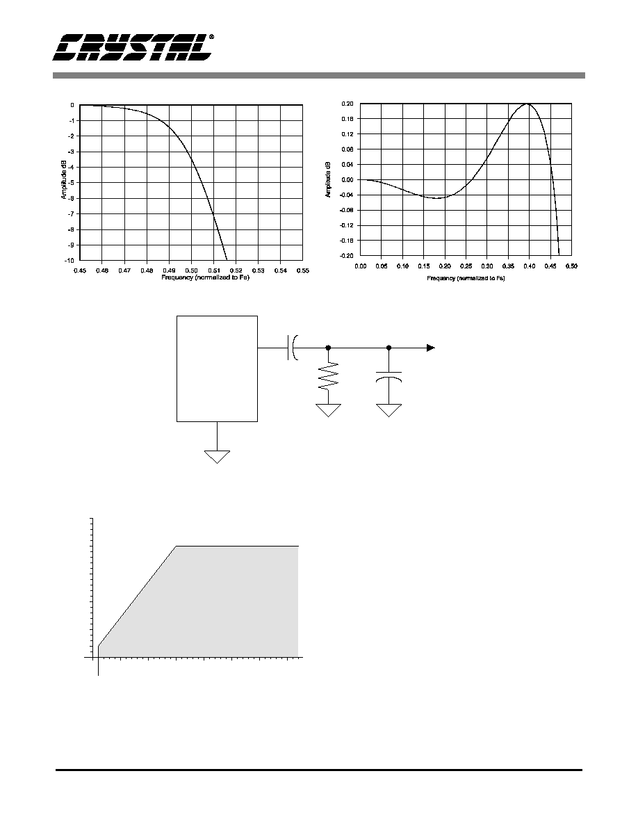
LIST OF FIGURES
Figure 1.
Serial Mode Input Timing ............................................................................................... 9
Figure 2.
Control Port Timing - Two-Wire Format ....................................................................... 10
Figure 3.
Control Port Timing - SPI Format ................................................................................. 11
Figure 4.
Typical Connection Diagram ........................................................................................ 12
Figure 5.
Control Port Timing, Two-Wire Format ........................................................................ 25
Figure 6.
Control Port Timing, SPI Format .................................................................................. 25
Figure 7.
Base-Rate Stopband Rejection .................................................................................... 27
Figure 8.
Base-Rate Transition Band .......................................................................................... 27
Figure 9.
Base-Rate Transition Band (Detail) ............................................................................. 27
Figure 10. Base-Rate Passband Ripple ........................................................................................ 27
Figure 11. High-Rate Stopband Rejection .................................................................................... 27
Figure 12. High-Rate Transition Band ........................................................................................... 27
Figure 13. High-Rate Transition Band (Detail) .............................................................................. 28
Figure 14. High-Rate Passband Ripple ......................................................................................... 28
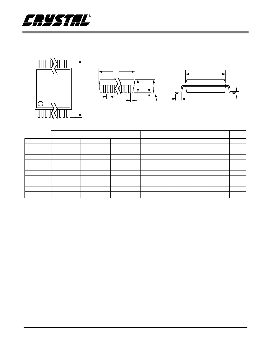
Figure 15. Output Test Load ......................................................................................................... 28
Figure 16. Maximum Loading ........................................................................................................ 28
Figure 17. CS4360 Format 0 - Left Justified upto 24-bit Data ....................................................... 29
Figure 18. CS4360 Format 1 - I
2
S upto 24-bit Data ...................................................................... 29
Figure 19. CS4360 Format 2 - Right Justified 16-bit Data ............................................................ 29
Figure 20. CS4360 Format 3 - Right Justified 24-bit Data ............................................................ 29
Figure 21. CS4360 Format 4 - Right Justified 20-bit Data ............................................................ 30

CS4360
4
DS517PP1
Figure 22. CS4360 Format 5 - Right Justified 18-bit Data ............................................................ 30
Figure 23. De-Emphasis Curve ..................................................................................................... 30
Figure 24. ATAPI Block Diagram .................................................................................................. 31
LIST OF TABLES
Table 1. Digital Interface Formats - Control Port Mode .................................................................... 14
Table 2. ATAPI Decode .................................................................................................................... 16
Table 3. Example Digital Volume Settings ....................................................................................... 17
Table 4. Digital Interface Formats - Stand Alone Mode.................................................................... 21
Table 5. Mode Selection................................................................................................................... 21
Table 6. Single-Speed Mode Common Clock Frequencies.............................................................. 22
Table 7. Double-Speed Mode Common Clock Frequencies ............................................................ 22
Table 8. Quad-Speed Mode Common Clock Frequencies............................................................... 22

CS4360
DS517PP1
5
1.
CHARACTERISTICS AND SPECIFICATIONS
ANALOG CHARACTERISTICS
(Full-Scale Output Sine Wave, 997 Hz; for Single-Speed Mode,
Fs = 48 kHz, SCLK = 3.072 MHz, MCLK = 12.288 MHz; for Double-Speed Mode Fs = 96 kHz, SCLK = 6.144 MHz,
MCLK = 12.288 MHz; for Quad-Speed Mode Fs = 192 kHz, SCLK = 12.288 MHz, MCLK = 24.576 MHz; Measure-
ment Bandwidth 10 Hz to 20 kHz, unless otherwise specified. Test load R
L
= 10 k
,
C
L
= 10 pF (see Figure 15).
VA = VD = VLS = VLC),
Notes: 1. CS4360-KS/-KZ parts are tested at 25 ∞C.
2. One-half LSB of triangular PDF dither is added to data.
3. CS4360-BS/-BZ parts are tested at the extremes of the specified temperature range and Min/Max
performance numbers are guaranteed across the specified temperature range, T
A
. Typical numbers are
taken at 25 ∞C.
ANALOG CHARACTERISTICS
(Continued)
Parameter
VA = 5 V
VA = 3 V
Symbol
Min
Typ
Max
Min
Typ
Max
Unit
CS4360-KS/-KZ Dynamic Performance (Note 1)
Specified Temperature Range
T
A
-10
-
70
-10
-
70
∞C
Dynamic Range
(Note 2)
unweighted
A-Weighted
40 kHz Bandwidth
A-Weighted
TBD
TBD
-
99
102
100
-
-
-
TBD
TBD
-
94
97
97
-
-
-
dB
dB
dB
Total Harmonic Distortion + Noise
(Note 2)
0 dB
-20 dB
-60 dB
THD+N
-
-
-
-
-91
-79
-39
TBD
-
-
-
-
-
-91
-74
-34
TBD
-
-
dB
dB
dB
Interchannel Isolation
(1 kHz)
-
102
-
-
102
-
dB
CS4360-BS/-BZ Dynamic Performance (Note 3)
Specified Temperature Range
T
A
-40
-
85
-40
-
85
∞C
Dynamic Range
(Note 2)
unweighted
A-Weighted
40 kHz Bandwidth
A-Weighted
TBD
TBD
-
99
102
100
-
-
-
TBD
TBD
-
94
97
97
-
-
-
dB
dB
dB
Total Harmonic Distortion + Noise
(Note 2)
0 dB
-20 dB
-60 dB
THD+N
-
-
-
-
-91
-79
-39
TBD
-
-
-
-
-
-91
-74
-34
TBD
-
-
dB
dB
dB
Interchannel Isolation
(1 kHz)
-
102
-
-
102
-
dB
Parameter
Symbol
Min
Typ
Max
Unit
Combined Digital and On-chip Analog Filter Response - Single-Speed Mode (Note 4)
Passband
(Note 5)
to -0.05 dB corner
to -3 dB corner
0
0
-
-
.4535
.4998
Fs
Fs
Frequency Response 10 Hz to 20 kHz
-.02
-
+.035
dB
StopBand
.5465
-
-
Fs
CS4360
6
DS517PP1
Notes: 4. Filter response is guaranteed by design.
5. Response is clock dependent and will scale with Fs. Note that the response plots (Figures 9 - 12) have
been normalized to Fs and can be de-normalized by multiplying the X-axis scale by Fs.
6. For Single-Speed Mode, the Measurement Bandwidth is .5465 Fs to 3 Fs.
For Double-Speed Mode, the Measurement Bandwidth is .577 Fs to 1.4 Fs.
7. De-emphasis is available only in Single-Speed Mode.
8. Refer to Figure 16.
StopBand Attenuation
(Note 6)
50
-
-
dB
Group Delay
tgd
-
9/Fs
-
s
Passband Group Delay Deviation
0 - 20 kHz
-
±0.36/Fs
-
s
De-emphasis Error (Relative to 1 kHz)
Fs = 32 kHz
Control Port Mode
Fs = 44.1 kHz
(Note 7)
Fs = 48 kHz
Fs = 32 kHz
Stand-Alone Mode
Fs = 44.1 kHz
Fs = 48 kHz
-
-
-
-
-
-
-
-
-
-
-
-
+.2/-.1
+.05/-.14
+0/-.22
+1.5/-0
+.05/-.14
+.2/-.4
dB
dB
dB
dB
dB
dB
Combined Digital and On-chip Analog Filter Response - Double-Speed Mode (Note 4)
Passband
(Note 5)
to -0.1 dB corner
to -3 dB corner
0
0
-
-
.4621
.4982
Fs
Fs
Frequency Response 10 Hz to 20 kHz
-0.1
-
0
dB
StopBand
.577
-
-
Fs
StopBand Attenuation
(Note 6)
55
-
-
dB
Group Delay
tgd
-
4/Fs
-
s
Passband Group Delay Deviation
0 - 20 kHz
-
±0.23/Fs
-
s
Combined Digital and On-chip Analog Filter Response - Quad-Speed Mode (Note 4)
Passband
(Note 5)
to -3 dB corner
0
-
.25
Fs
Frequency Response 10 Hz to 20 kHz
-0.7
-
0
dB
Group Delay
tgd
-
1.5/Fs
-
s
Parameters
Symbol
Min
Typ
Max
Units
Analog Output
Full Scale Output Voltage
0.60∑V
A
0.66∑V
A
0.72∑V
A
Vpp
Quiescent Voltage
V
Q
-
0.5∑V
A
-
VDC
Quiescent Pin External Load
I
Q
-
-
TBD
VDC
Interchannel Gain Mismatch
-
0.1
-
dB
Gain Drift
-
100
-
ppm/∞C
AC-Load Resistance
(Note 8)
R
L
3
-
-
k
Load Capacitance
C
L
-
-
100
pF
Output Impedance
Z
OUT
-
100
-
Parameter
Symbol
Min
Typ
Max
Unit
CS4360
DS517PP1
7
POWER AND THERMAL CHARACTERISTICS
Notes: 9. Current consumption is directly proportional to Fs. Typ and Max values are based on highest FS
10. I
LC
measured with no external loading on pin 12 (SDA).
11. Power down mode is defined as RST = Low with all clock and data lines held static.
12. Valid with the recommended capacitor values on FILT+ and V
CM
as shown in Figure 4.
DIGITAL CHARACTERISTICS
(For -KS & -KZ parts T
A
= -10 to +70∞C; for -BS & -BZ parts T
A
= -40
to +85∞C; VD = 2.0 V - 5.5 V, VLC = VLS = 1.8 V - 5.5 V)
Parameters
Symbol
Min
Typ
Max
Units
Power Supplies
Power Supply Current
normal operation, All Supplies = 5 V
(Note 9)
All Supplies = 3 V
Interface current (Note 10)
power-down state (all supplies) (Note 11)
I
A
I
D
I
A
I
D
I
LS
I
LC
I
pd
-
-
-
-
-
-
-
22
25
21
14
0.002
0.002
0.016
-
-
-
-
-
-
-
mA
mA
mA
mA
mA
mA
mA
Power Dissipation
(Note 9)
All Supplies = 5 V
normal operation
power-down (Note 11)
All Supplies = 3 V
normal operation
power-down (Note 11)
-
-
-
-
235
0.080
105
0.048
TBD
-
TBD
-
mW
mW
mW
mW
Package Thermal Resistance
SOIC (-KS & -BS)
TSSOP (-KZ & -BZ)
JA
JC
JA
JC
-
-
-
-
TBD
TBD
TBD
TBD
-
-
-
-
∞C/Watt
∞C/Watt
∞C/Watt
∞C/Watt
Power Supply Rejection Ratio (1 kHz)
(Note 12)
(60 Hz)
PSRR
PSRR
-
-
60
40
-
-
dB
dB
Parameters
Symbol Min Typ
Max
Units
High-Level Input Voltage
Serial Audio Data Port
Control Port
V
IH
V
IH
70%
70%
-
-
-
-
VLS
VLC
Low-Level Input Voltage
Serial Audio Data Port
Control Port
V
IL
-
-
-
-
20%
20%
VLS
VLC
Input Leakage Current
I
in
-
-
±10
µ
A
Input Capacitance
-
8
-
pF
Maximum MUTEC Drive Current
-
3
-
mA
MUTEC High-Level Output Voltage
V
OH
VA
V
MUTEC Low-Level Output Voltage
V
OL
0
V
CS4360
8
DS517PP1
ABSOLUTE MAXIMUM RATINGS
(GND = 0V; all voltages with respect to ground.)
WARNING: Operation at or beyond these limits may result in permanent damage to the device. Normal operation is
not guaranteed at these extremes.
RECOMMENDED OPERATING CONDITIONS
(GND = 0V; all voltages with respect to ground.)
13. Applies to pins 2, 3, 4, 5, 6, and 7.
14. Applies to pins 10, 11, 12, and 13.
Parameters
Symbol
Min
Max
Units
DC Power Supply
Analog power
Digital power
Serial Audio Data Interface power
Control Port Interface power
VA
VD
VLS
VLC
-0.3
-0.3
-0.3
-0.3
6.0
6.0
6.0
6.0
V
V
V
V
Input Current, Any Pin Except Supplies
I
in
-
±10
mA
Digital Input Voltage
Serial audio data interface
Control port interface
V
IND_S
V
IND_C
-0.3
-0.3
VLS + 0.4
VLC + 0.4
V
V
Ambient Operating Temperature (power applied)
T
A
-55
125
∞C
Storage Temperature
T
stg
-65
150
∞C
Parameters
Symbol Min Typ
Max
Units
DC Power Supply
Analog Power
Digital Power
Serial Audio Data Interface Power (Note 13)
Control Port Interface Power (Note 14)
VA
VD
VLS
VLC
2.7
2.0
1.8
1.8
5
5
5
5
5.5
VA
5.5
5.5
V
V
V
V
CS4360
DS517PP1
9
SWITCHING CHARACTERISTICS
(For -KS & -KZ parts T
A
= -10 to +70∞C; for -BS & -BZ parts T
A
=
-40 to +85∞C; VLS = 1.7 V to 5.5 V; Inputs: Logic 0 = 0 V, Logic 1 = VLS CL = 20 pF)
Notes: 15. This serial clock is available only in Control Port Mode when the MCLK Divide bit is enabled.
Parameters
Symbol Min
Typ
Max
Units
Input Sample Rate
Single-Speed Mode
Double-Speed Mode
Quad-Speed Mode
F
s
F
s
F
s
4
50
100
-
-
-
50
100
200
kHz
kHz
kHz
LRCK Duty Cycle
45
50
55
%
MCLK Duty Cycle
40
50
60
%
SCLK Frequency
-
-
MCLK/2
Hz
SCLK Frequency
Note 15
-
-
MCLK/4
Hz
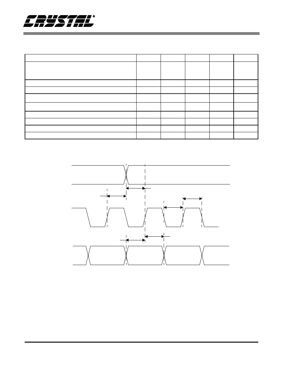
SCLK rising to LRCK edge delay
t
slrd
20
-
-
ns
SCLK rising to LRCK edge setup time
t
slrs
20
-
-
ns
SDATA valid to SCLK rising setup time
t
sdlrs
20
-
-
ns
SCLK rising to SDATA hold time
t
sdh
20
-
-
ns
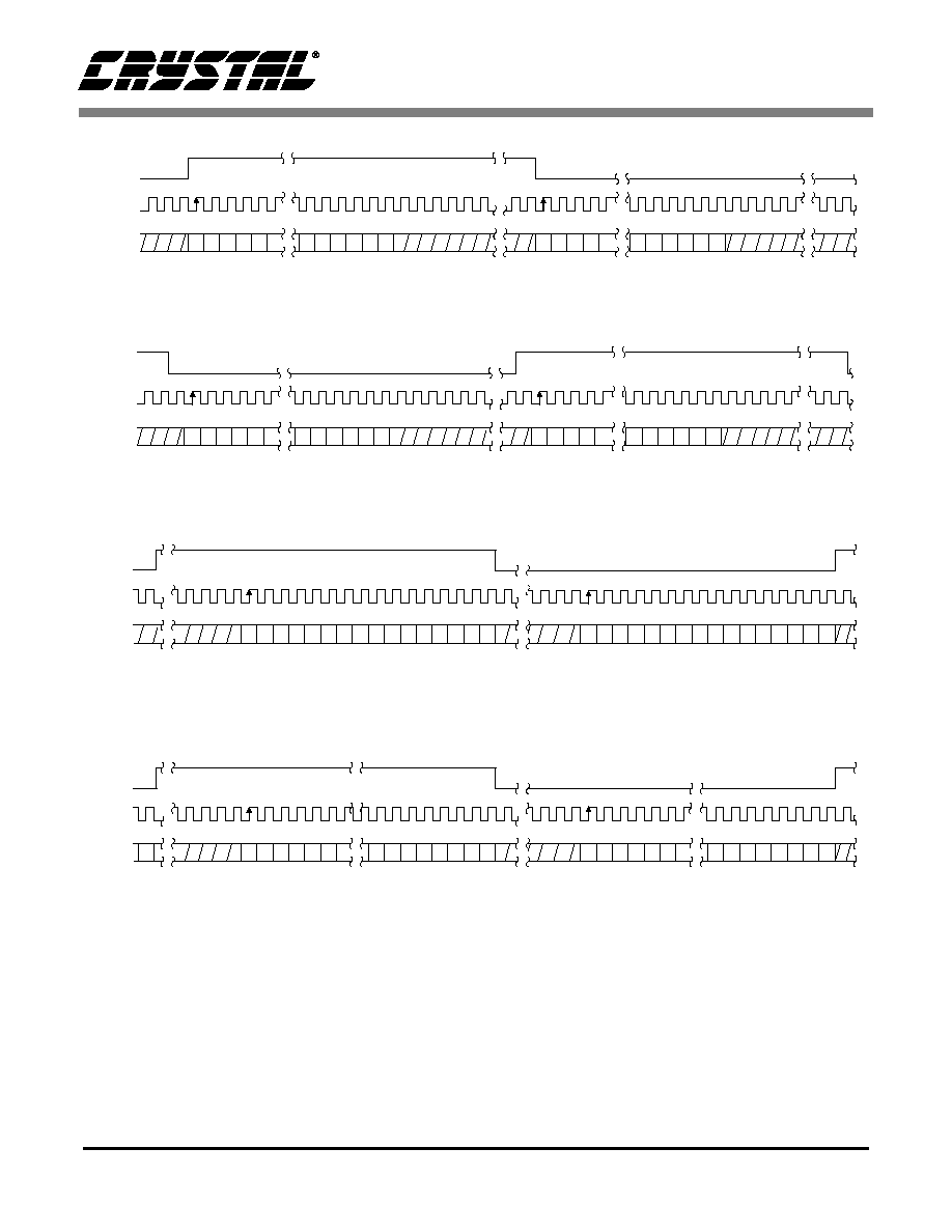
Figure 1. Serial Mode Input Timing
sclkh
t
slrs
t
slrd
t
sdlrs
t
sdh
t
sclkl
t
SDATA
SCLK
LRCK

CS4360
10
DS517PP1
SWITCHING CHARACTERISTICS- CONTROL PORT- TWO-WIRE FORMAT
(Note 16) (For -KS & -KZ parts T
A
= -10 to +70∞C; for -BS & -BZ parts T
A
= -40 to +85∞C; VLC = 1.7 V - 5.5 V;
Inputs: Logic 0 = GND, Logic 1 = VLC, C
L
= 30 pF)
Notes: 16. The Two-Wire Format is compatible with the I
2
C protocol.
17. Data must be held for sufficient time to bridge the transition time, t
fc
, of SCL.
18. The acknowledge delay is based on MCLK and can limit the maximum transaction speed.
19.
for Single-Speed Mode,
for Double-Speed Mode,
for Quad-Speed Mode.
Parameter
Symbol
Min
Max
Unit
SCL Clock Frequency
f
scl
-
100
kHz
RST Rising Edge to Start
t
irs
500
-
ns
Bus Free Time Between Transmissions
t
buf
4.7
-
µs
Start Condition Hold Time (prior to first clock pulse)
t
hdst
4.0
-
µs
Clock Low time
t
low
4.7
-
µs
Clock High Time
t
high
4.0
-
µs
Setup Time for Repeated Start Condition
t
sust
4.7
-
µs
SDA Hold Time from SCL Falling
(Note 17)
t
hdd
0
-
µs
SDA Setup time to SCL Rising
t
sud
250
-
ns
Rise Time of SCL and SDA
t
rc
, t
rc
-
1
µs
Fall Time SCL and SDA
t
fc
, t
fc
-
300
ns
Setup Time for Stop Condition
t
susp
4.7
-
µs
Acknowledge Delay from SCL Falling
(Note 18)
t
ack
-
(Note 19)
ns
5
256
Fs
◊
---------------------
5
128
Fs
◊
---------------------
5
64
Fs
◊
------------------
t
buf
t
hdst
t
lo w
t
hdd
t
high
t
sud
Stop
Sta rt
S D A
S C L
t
irs
R S T
t
hdst
t
rc
t
fc
t sust
t susp
Sta rt
Stop
R e p e ate d
t
rd
t
fd
t
ack
Figure 2. Control Port Timing - Two-Wire Format
CS4360
DS517PP1
11
SWITCHING CHARACTERISTICS - CONTROL PORT - SPI FORMAT
(For -KS & -KZ parts T
A
= -10 to +70∞C; for -BS & -BZ parts T
A
= -40 to +85∞C; VLC = 1.7 V - 5.5 V; Inputs: Logic
0 = GND, Logic 1 = VLC, C
L
= 30 pF)
Notes: 20. t
spi
only needed before first falling edge of CS after RST rising edge. t
spi
= 0 at all other times.
21. Data must be held for sufficient time to bridge the transition time of CCLK.
22. For F
SCK
< 1 MHz.
Parameter
Symbol
Min
Max
Unit
CCLK Clock Frequency
f
sclk
-
6
MHz
RST Rising Edge to CS Falling
t
srs
500
-
ns
CCLK Edge to CS Falling
(Note 20)
t
spi
500
-
ns
CS High Time Between Transmissions
t
csh
1.0
-
µs
CS Falling to CCLK Edge
t
css
20
-
ns
CCLK Low Time
t
scl
66
-
ns
CCLK High Time
t
sch
66
-
ns
CDIN to CCLK Rising Setup Time
t
dsu
40
-
ns
CCLK Rising to DATA Hold Time
(Note 21)
t
dh
15
-
ns
Rise Time of CCLK and CDIN
(Note 22)
t
r2
-
100
ns
Fall Time of CCLK and CDIN
(Note 22)
t
f2
-
100
ns
t r2
t f2
t dsu t
dh
t
sch
t scl
CS
CCLK
CDIN
t css
t
csh
t spi
t srs
RST
Figure 3. Control Port Timing - SPI Format

CS4360
12
DS517PP1
2.
TYPICAL CONNECTION DIAGRAM
21
Digital
Audio
Source
VLS
GND
CS4360
MCLK
VA
AOUT1A
2
3
4
8
0.1 µF
+
1 µF
+3 V to +5 V *
µ C/
Mode
Configuration
13
10
12
SDIN1
5
DIF1/SCL/CCLK
DIF0/SDA/CDIN
M1/AD0/CS
RST
MUTEC1
OPTIONAL
MUTE
CIRCUIT
3.3 µF
0.1 µ F
AOUTA1
C =
4
Fs(R 560)
L
R L
+
+
16
15
FILT+
VQ
11
15
M2
7
6
LRCK1
SCLK1
SDIN3
SDIN2
3.3 µF
10 k
C
560
+
28
27
3.3 µF
10 k
C
560
+
26
AOUTB1
R L
OPTIONAL
MUTE
CIRCUIT
AOUTA2
R L
3.3 µF
10 k
C
560
+
25
24
3.3 µF
10 k
C
560
+
23
AOUTB2
R L
OPTIONAL
MUTE
CIRCUIT
AOUTA3
R L
3.3 µF
10 k
C
560
+
18
20
3.3 µF
10 k
C
560
+
19
AOUTB3
R L
AOUT1B
0.1 µ F
3.3 µF
AOUT2A
MUTEC2
AOUT2B
AOUT3A
MUTEC3
AOUT3B
VD
0.1 µF
+
1 µF
GND
9
0.1 µF
+1.8 V to +5 V *
VLC
0.1 µF
+1.8 V to +5 V *
RL+560
+3 V to +5 V *
* All supplies can be tied together
22
1
14
SDIN4
LRCK2
SCLK2
4
4
4
Figure 4. Typical Connection Diagram

CS4360
DS517PP1
13
3.
REGISTER QUICK REFERENCE
Addr
Function
7
6
5
4
3
2
1
0
1h
Mode Control 1
AMUTE
DIF2
DIF1
DIF0
DEM1
DEM0
FM1
FM0
default
1
0
0
0
0
0
0
0
2h
Invert Signal
Reserved
Reserved
INV_B3
INV_A3
INV_B2
INV_A2
INV_B1
INV_A1
default
0
0
0
0
0
0
0
0
3h
Mixing Control P1
Reserved
Reserved
Reserved
Reserved P1ATAPI3 P1ATAPI2 P1ATAPI1 P1ATAPI0
default
0
0
0
0
1
0
0
1
4h
Mixing Control P2
Reserved
Reserved
Reserved
Reserved P2ATAPI3 P2ATAPI2 P2ATAPI1 P2ATAPI0
default
0
0
0
0
1
0
0
1
5h
Mixing Control P3
Reserved
Reserved
Reserved
Reserved P3ATAPI3 P3ATAPI2 P3ATAPI1 P3ATAPI0
default
0
0
0
0
1
0
0
1
6h
Volume Control A1
A1_MUTE A1_VOL6
A1_VOL5
A1_VOL4
A1_VOL3
A1_VOL2
A1_VOL1
A1_VOL0
default
0
0
0
0
0
0
0
0
7h
Volume Control B1
B1_MUTE B1_VOL6
B1_VOL5
B1_VOL4
B1_VOL3
B1_VOL2
B1_VOL1
B1_VOL0
default
0
0
0
0
0
0
0
0
8h
Volume Control A2
A2_MUTE A2_VOL6
A2_VOL5
A2_VOL4
A2_VOL3
A2_VOL2
A2_VOL1
A2_VOL0
default
0
0
0
0
0
0
0
0
9h
Volume Control B2
B2_MUTE B2_VOL6
B2_VOL5
B2_VOL4
B2_VOL3
B2_VOL2
B2_VOL1
B2_VOL0
default
0
0
0
0
0
0
0
0
0Ah
Volume Control A3
A3_MUTE A3_VOL6
A3_VOL5
A3_VOL4
A3_VOL3
A3_VOL2
A3_VOL1
A3_VOL0
default
0
0
0
0
0
0
0
0
0Bh
Volume Control B3
B3_MUTE B3_VOL6
B3_VOL5
B3_VOL4
B3_VOL3
B3_VOL2
B3_VOL1
B3_VOL0
default
0
0
0
0
0
0
0
0
0Ch
Mode Control 2
SZC1
SZC0
CPEN
PDN
POPG
FREEZE
MCLKDIV SNGLVOL
default
1
0
0
1
1
0
0
0
0Dh
Revision Indicator
Reserved
Reserved
Reserved
Reserved
REV3
REV2
REV1
REV0
default
0
0
0
0
X
X
X
X

CS4360
14
DS517PP1
4.
REGISTER DESCRIPTIONS
Note: All registers are read/write in Two-Wire mode and write only in SPI, unless otherwise noted.
4.1
Mode Control 1 (address 01h)
4.1.1
AUTO-MUTE (AMUTE)
Default = 1
0 - Disabled
1 - Enabled
Function:
The Digital-to-Analog converter output will mute following the reception of 8192 consecutive audio
samples of static 0 or -1. A single sample of non-static data will release the mute. Detection and
muting is done independently for each channel. The quiescent voltage on the output will be retained
and the Mute Control pin will go active during the mute period. The muting function is affected, similar
to volume control changes, by the Soft and Zero Cross bits in the Power and Muting Control register.
4.1.2
DIGITAL INTERFACE FORMAT (DIF)
Default
= 000
- Format 0 (Left Justified, up to 24-bit data)
Function:
The required relationship between the Left/Right clock, serial clock and serial data is defined by the
Digital Interface Format and the options are detailed in Figures 17-22.
7
6
5
4
3
2
1
0
AMUTE
DIF2
DIF1
DIF0
DEM1
DEM0
FM1
FM0
1
0
0
0
0
0
0
0
DIF2
DIF1
DIF0
DESCRIPTION
Format
FIGURE
0
0
0
Left Justified, up to 24-bit data,
0
17
0
0
1
I
2
S, up to 24-bit data
1
18
0
1
0
Right Justified, 16-bit data
2
19
0
1
1
Right Justified, 24-bit data
3
20
1
0
0
Right Justified, 20-bit data
4
21
1
0
1
Right Justified, 18-bit data
5
22
1
1
0
Reserved
1
1
1
Reserved
Table 1. Digital Interface Formats - Control Port Mode

CS4360
DS517PP1
15
4.1.3
DE-EMPHASIS CONTROL (DEM)
Default = 00
00 - Disabled
01 - 44.1 kHz
10 - 48 kHz
11 - 32 kHz
Function:
Selects the appropriate digital filter to maintain the standard 15
µ
s/50
µ
s digital de-emphasis filter re-
sponse at 32, 44.1 or 48 kHz sample rates. (see Figure 23)
Note:
De-emphasis is only available in Single-Speed Mode.
4.1.4
FUNCTIONAL MODE (FM)
Default = 00
00 - Single-Speed Mode (2 to 50 kHz sample rates)
01 - Double-Speed Mode (50 to 100 kHz sample rates)
10 - Quad-Speed Mode (100 to 200 kHz sample rates)
11 - Reserved
Function:
Selects the required range of input sample rates.
4.2
Invert Signal (address 02h)
4.2.1
INVERT SIGNAL POLARITY (INV_XX)
Default = 0
0 - Disabled
1 - Enabled
Function:
When enabled, these bits invert the signal polarity for each of their respective channels.
4.3
Mixing Control Pair 1 (Channels A1 & B1) (address 03h)
Mixing Control Pair 2 (Channels A2 & B2) (address 04h)
Mixing Control Pair 3 (Channels A3 & B3) (address 05h)
7
6
5
4
3
2
1
0
Reserved
Reserved
INV_B3
INV_A3
INV_B2
INV_A2
INV_B1
INV_A1
0
0
0
0
0
0
0
0
7
6
5
4
3
2
1
0
Reserved
Reserved
Reserved
Reserved
PxATAPI3
PxATAPI2
PxATAPI1
PxATAPI0
0
0
0
0
1
0
0
1
CS4360
16
DS517PP1
4.3.1
ATAPI CHANNEL MIXING AND MUTING (ATAPI)
Default = 1001 - AOUTAx = L, AOUTBx = R (Stereo)
Function:
The CS4360 implements the channel mixing functions of the ATAPI CD-ROM specification. Refer to
Table 2 and Figure 24 for additional information.
Note:
All mixing functions occur prior to the digital volume control. Mixing only occurs in channel pairs.
4.4
Volume Control (addresses 06h - 0Bh)
4.4.1
MUTE (MUTE)
Default = 0
0 - Disabled
1 - Enabled
Function:
The Digital-to-Analog converter output will mute when enabled. The quiescent voltage on the output
will be retained. The muting function is effected, similar to attenuation changes, by the Soft and Zero
Cross bits. The MUTEC pin will go active during the mute period if the Mute function is enabled for
both channels in the pair.
ATAPI3
ATAPI2
ATAPI1
ATAPI0
AOUTAx
AOUTBx
0
0
0
0
MUTE
MUTE
0
0
0
1
MUTE
R
0
0
1
0
MUTE
L
0
0
1
1
MUTE
[(L+R)/2]
0
1
0
0
R
MUTE
0
1
0
1
R
R
0
1
1
0
R
L
0
1
1
1
R
[(L+R)/2]
1
0
0
0
L
MUTE
1
0
0
1
L
R
1
0
1
0
L
L
1
0
1
1
L
[(L+R)/2]
1
1
0
0
[(L+R)/2]
MUTE
1
1
0
1
[(L+R)/2]
R
1
1
1
0
[(L+R)/2]
L
1
1
1
1
[(L+R)/2]
[(L+R)/2]
Table 2. ATAPI Decode
7
6
5
4
3
2
1
0
xx_MUTE
xx_VOL6
xx_VOL5
xx_VOL4
xx_VOL3
xx_VOL2
xx_VOL1
xx_VOL0
0
0
0
0
1
0
0
1
CS4360
DS517PP1
17
4.4.2
VOLUME CONTROL
(XX_VOL)
Default = 0
Function:
The Digital Volume Control registers allow independent control of the signal levels in 1 dB increments
from 0 to -119 dB. Volume settings are decoded as shown in Table 3. The volume changes are im-
plemented as dictated by the Soft Ramp and Zero Cross bits. All volume settings less than -119 dB
are equivalent to enabling the MUTE bit.
4.5
Mode Control 2 (address 0Dh)
4.5.1
SOFT RAMP AND ZERO CROSS CONTROL (SZC)
Default = 10
00 - Immediate Change
01 - Zero Cross
10 - Soft Ramp
11 - Soft Ramp and Zero Cross
Function:
Immediate Change
When Immediate Change is selected all level changes will be implemented immediately in one step.
Zero Cross
Zero Cross Enable dictates that signal level changes, either by attenuation changes or muting, will
occur on a signal zero crossing to minimize audible artifacts. The requested level change will occur
after a timeout period between 512 and 1024 sample periods (10.7 ms to 21.3 ms at 48 kHz sample
rate) if the signal does not encounter a zero crossing. The zero cross function is independently mon-
itored and implemented for each channel.
Soft Ramp
Soft Ramp allows level changes, both muting and attenuation, to be implemented by incrementally
ramping, in 1/8 dB steps, from the current level to the new level at a rate of 1 dB per 8 left/right clock
periods.
Soft Ramp and Zero Cross
Soft Ramp and Zero Cross dictates that signal level changes, either by attenuation changes or mut-
ing, will occur in 1/8 dB steps and will be implemented on successive signal zero crossings. The 1/8
dB level changes will occur after timeout periods between 512 and 1024 sample periods (10.7 ms to
21.3 ms at 48 kHz sample rate) if the signal does not encounter zero crossings. The zero cross func-
tion is independently monitored and implemented for each channel.
Binary Code
Decimal Value
Volume Setting
0001010
0
dB
0010100
-20
-20 dB
0101000
-40
-40 dB
0111100
-60
-60 dB
1011010
-90
-90 dB
Table 3. Example Digital Volume Settings
7
6
5
4
3
2
1
0
SZC1
SZC0
CPEN
PDN
POPG
FREEZE
MCLKDIV
SNGLVOL
1
0
0
1
1
0
0
0

CS4360
18
DS517PP1
4.5.2
CONTROL PORT ENABLE (CPEN)
Default = 0
0 - Disabled
1 - Enabled
Function:
The Control Port will become active and reset to the default settings when this function is enabled.
4.5.3
POWER DOWN (PDN)
Default = 1
0 - Disabled
1 - Enabled
Function:
The entire device will enter a low-power state when this function is enabled, and the contents of the
control registers are retained in this mode. The power-down bit defaults to `enabled' on power-up and
must be disabled before normal operation in Control Port mode can occur.
4.5.4
POPGUARDÆ TRANSIENT CONTROL (POPG)
Default = 1
0 - Disabled
1 - Enabled
Function:
The PopGuard
Æ
Transient Control allows the quiescent voltage to slowly ramp to and from 0 volts to
the quiescent voltage during power-on or power-off when this function is enabled. Please see section
6.4 for implementation details.
4.5.5
FREEZE CONTROLS (FREEZE)
Default = 0
0 - Disabled
1 - Enabled
Function:
This function allows modifications to be made to the registers without the changes taking effect until
the FREEZE is disabled. To make multiple changes in the control port registers take effect simulta-
neously, enable the FREEZE bit, make all register changes, then disable the FREEZE bit.
4.5.6
MASTER CLOCK DIVIDE ENABLE (MCLKDIV)
Default = 0
0 - Disabled
1 - Enabled
Function:
The MCLKDIV bit enables a circuit which divides the externally applied MCLK signal by 2 prior to all
other internal circuitry.

CS4360
DS517PP1
19
4.5.7
SINGLE VOLUME CONTROL (SNGLVOL)
Default = 0
0 - Disabled
1 - Enabled
Function:
The individual channel volume levels are independently controlled by their respective Volume Control
Bytes when this function is disabled. The volume on all channels is determined by the A1 Channel
Volume Control Byte, and the other Volume Control Bytes are ignored when this function is enabled.
4.6
Revision Register (Read Only) (address 0Dh)
4.6.1
REVISION INDICATOR (REV) [READ ONLY]
Default = none
0001 - Revision A
0010 - Revision B
0011 - Revision C
etc.
Function:
This read-only register indicates the revision level of the device.
7
6
5
4
3
2
1
0
Reserved
Reserved
Reserved
Reserved
REV3
REV2
REV1
REV0
0
0
0
0
X
X
X
X

CS4360
20
DS517PP1
5.
PIN DESCRIPTION
Pin Name
#
Pin Description
VLS
1
Serial Audio Interface Power (
Input) - Determines the required signal level for the serial audio inter-
face. Refer to the Recommended Operating Conditions for appropriate voltages. Applies to pins 2-7.
SDIN1
SDIN2
SDIN3
2
3
4
Serial Audio Data Input (
Input) - Input for two's complement serial audio data. SDIN1 corresponds to
AOUT1x, SDIN2 corresponds to AOUT2x and SDIN3 corresponds to AOUT3x.
SCLK
5
Serial Clock (
Input) - Serial clock for the serial audio interface.
LRCK
6
Left / Right Clock (
Input) - Determines which channel, Left or Right, is currently active on the serial
audio data line. The frequency of the left/right clock must be at the audio sample rate, Fs.
MCLK
7
Master Clock (
Input) - Clock source for the delta-sigma modulator and digital filters. Table 6 illustrates
several standard audio sample rates and the required master clock frequency.
VD
8
Digital Power (
Input) - Positive power supply for the digital section. Refer to the Recommended Operat-
ing Conditions for appropriate voltages.
GND
9
21
Ground (
Input) - Ground reference. Should be connected to analog ground.
RST
10
Reset (
Input) - The device enters a low power mode and all internal registers are reset to their default
settings when low. The control port cannot be accessed when Reset is low.
VLC
14
Control Port Interface Power (
Input) - Determines the required signal level for the control port and pro-
vides power for bidirectional control port pins. Refer to the Recommended Operating Conditions for
appropriate voltages. Applies to pins 10-13 and 15.
FILT+
16
Positive Voltage Reference (
Output) - Positive reference voltage for the internal sampling circuits.
Requires the capacitive decoupling to GND as shown in the Typical Connection Diagram.
Serial Audio Power
VLS
MUTEC1 Mute Control 1
Serial Data Input 1
SDIN1
AOUTA1 Analog Output A1
Serial Data Input 2
SDIN2
AOUTB1 Analog Output B1
Serial Data Input 3
SDIN3
MUTEC2 Mute Control 2
Serial Clock
SCLK
AOUTA2 Analog Output A2
Left/Right Clock
LRCK
AOUTB2 Analog Output B2
Master Clock
MCLK
VA
Analog Power
Digital Power
VD
GND
Ground
Ground
GND
AOUTA3 Analog Output A3
Reset
RST
AOUTB3 Analog Output B3
DIF1 / SCL/ CCLK DIF1/SCL/CCLK
MUTEC3 Mute Control 3
DIF0 / SDA / CDIN
DIF0/SDA/CDIN
VQ
Quiescent Voltage
Mode1 / AD0 / CS
M1/AD0/CS
FILT+
Positive Voltage Reference
Control Port Power
VLC
M2
Mode 2
1
2
3
4
5
6
7
8
9
10
11
12
5
1
2
6
24
23
22
21
20
19
18
17
16
15
14
13
25
26
27
28
CS4360
DS517PP1
21
VQ
17
Quiescent Voltage (
Output) - Filter connection for internal quiescent voltage. VQ must be capacitively
coupled to analog ground, as shown in the Typical Connection Diagram. The nominal voltage level is
specified in the Analog Characteristics and Specifications section. VQ presents an appreciable source
impedance and any current drawn from this pin will alter device performance. However, VQ can be used
to bias the analog circuitry assuming there is no AC signal component and the DC current is less than
the maximum specified in the Analog Characteristics and Specifications section.
VA
22
Analog Power (
Input) - Positive power supply for the analog section. Refer to the Recommended Oper-
ating Conditions for appropriate voltages.
AOUTA1
AOUTB1
AOUTA2
AOUTB2
AOUTA3
AOUTB3
19
20
23
24
26
27
Analog Outputs (
Output) - The full scale analog line output level is specified in the Analog Characteris-
tics specifications table.
MUTEC1
MUTEC2
MUTEC3
18
25
28
Mute Control (
Output) - The Mute Control pin goes high during power-up initialization, reset, muting,
power-down or if the master clock to left/right clock frequency ratio is incorrect. This pin is intended to be
used as a control for an external mute circuit to prevent the clicks and pops that can occur in any single
supply system. The use of an external mute circuit is not mandatory but may be desired for designs
requiring the absolute minimum in extraneous clicks and pops.
Control Port
Definitions
SCL/CCLK
11
Serial Control Port Clock (
Input) - Serial clock for the serial control port. Requires an external pull-up
resistor to the logic interface voltage in Two-Wire mode as shown in the Typical Connection Diagram.
SDA/CDIN
12
Serial Control Data (
Input/Output) - SDA is a data I/O line in Two-Wire format and requires an external
pull-up resistor to the logic interface voltage, as shown in the Typical Connection Diagram. CDIN is the
input data line for the control port interface in SPI format.
AD0/CS
13
Address Bit 0 (Two-Wire) / Control Port Chip Select (SPI) (
Input/Output) - AD0 is a chip address pin
Two-Wire format; CS is the chip select signal for SPI format.
Stand-Alone
Definitions
DIF1
DIF0
11
12
Digital Interface Format (
Input) - The required relationship between the Left/Right clock, serial clock
and serial data is defined by the Digital Interface Format selection. Refer to Table 4.
M1
M2
13
15
Mode Selection (
Input) - Determines the operational mode of the device as detailed in Table 5.
DIF1
DIF0
DESCRIPTION
0
0
Left Justified, up to 24-bit data
0
1
I
2
S, up to 24-bit data
1
0
Right Justified, 16-bit data
1
1
Right Justified, 24-bit data
Table 4. Digital Interface Formats - Stand Alone Mode
M2
M1
MODE
0
0
Single-Speed without de-emphasis (4 to 50 kHz sample rates)
0
1
Single-Speed with de-emphasis (32 to 48 kHz sample rates)
1
0
Double-Speed (50 to 100 kHz sample rates)
1
1
Quad-Speed (100 to 200 kHz sample rates)
Table 5. Mode Selection

CS4360
22
DS517PP1
.
Sample Rate
(kHz)
MCLK (MHz)
256x
384x
512x
768x
1024x*
32
8.1920
12.2880
16.3840
24.5760
32.7680
44.1
11.2896
16.9344
22.5792
32.7680
45.1584
48
12.2880
18.4320
24.5760
36.8640
49.1520
* Requires MCLKDIV bit = 1
Table 6. Single-Speed Mode Common Clock Frequencies
Sample Rate
(kHz)
MCLK (MHz)
128x
192x
256x
384x
512x*
64
8.1920
12.2880
16.3840
24.5760
32.7680
88.2
11.2896
16.9344
22.5792
33.8688
45.1584
96
12.2880
18.4320
24.5760
36.8640
49.1520
* Requires MCLKDIV bit = 1
Table 7. Double-Speed Mode Common Clock Frequencies
Sample Rate
(kHz)
MCLK (MHz)
64x
96x
128x
192x
256x*
176.4
11.2896
16.9344
22.5792
33.8688
45.1584
192
12.2880
18.4320
24.5760
36.8640
49.1520
* Requires MCLKDIV bit = 1
Table 8. Quad-Speed Mode Common Clock Frequencies

CS4360
DS517PP1
23
6. APPLICATIONS
6.1
Grounding and Power Supply
Decoupling
As with any high resolution converter, the CS4360
requires careful attention to power supply and
grounding arrangements to optimize performance.
Figure 4 shows the recommended power arrange-
ment with VA, VD, VLS and VLC connected to
clean supplies. Decoupling capacitors should be lo-
cated as close to the device package as possible. If
desired, all supply pins may be connected to the
same supply, but a decoupling capacitor should still
be placed on each supply pin.
6.2
Oversampling Modes
The CS4360 operates in one of three oversampling
modes based on the input sample rate. Mode selec-
tion is determined by the FM pins in Stand-Alone
mode or the FM bits in Control Port mode. Single-
Speed mode supports input sample rates up to 50
kHz and uses a 128x oversampling ratio. Double-
Speed mode supports input sample rates up to 100
kHz and uses an oversampling ratio of 64x. Quad-
Speed mode supports input sample rates up to 200
kHz and uses an oversampling ratio of 32x.
6.3
Recommended Power-up Sequence
1. Hold RST low until the power supply, master,
and left/right clocks are stable. In this state, the
control port is reset to its default settings and VQ
will remain low.
2. Bring RST high. The device will remain in a low
power state with VQ low and will initiate the
Stand-Alone power-up sequence. The control port
will be accessible at this time. If Control Port oper-
ation is desired, write the CPEN bit prior to the
completion of the Stand-Alone power-up se-
quence, approximately 512 LRCK cycles in Sin-
gle-Speed Mode (1024 LRCK cycles in Double-
Speed Mode, and 2048 LRCK cycles in Quad-
Speed Mode). Writing this bit will halt the Stand-
Alone power-up sequence and initialize the control
port to its default settings. The desired register set-
tings can be loaded while keeping the PDN bit set
to 1.
3. If Control Port Mode is selected via the CPEN
bit, set the PDN bit to 0 which will initiate the pow-
er-up sequence, which requires approximately
50 µS when the POPG bit is set to 0. If the POPG
bit is set to 1, see Section 6.4 for total power-up
timing.
6.4
Popguard
Æ
Transient Control
The CS4360 uses a novel technique to minimize
the effects of output transients during power-up
and power-down. This technique, when used with
external DC-blocking capacitors in series with the
audio outputs, minimizes the audio transients com-
monly produced by single-ended single-supply
converters.
When the device is initially powered-up, the audio
outputs, AOUTAx and AOUTBx, are clamped to
GND. Following a delay of approximately 1000
sample periods, each output begins to ramp toward
the quiescent voltage. Approximately 10,000
left/right clock cycles later, the outputs reach VQ
and audio output begins. This gradual voltage
ramping allows time for the external DC-blocking
capacitor to charge to the quiescent voltage, mini-
mizing the power-up transient.
To prevent transients at power-down, the device
must first enter its power-down state. When this oc-
curs, audio output ceases and the internal output
buffers are disconnected from AOUTAx and
AOUTBx. In their place, a soft-start current sink is
substituted which allows the DC-blocking capaci-
tors to slowly discharge. Once this charge is dissi-
pated, the power to the device may be turned off
and the system is ready for the next power-on.
To prevent an audio transient at the next power-on,
it is necessary to ensure that the DC-blocking ca-
pacitors have fully discharged before turning off

CS4360
24
DS517PP1
the power or exiting the power-down state. If not, a
transient will occur when the audio outputs are ini-
tially clamped to GND. The time that the device
must remain in the power-down state is related to
the value of the DC-blocking capacitance. For ex-
ample, with a 3.3 µF capacitor, the minimum pow-
er-down time will be approximately 0.4 seconds.
Use of the Mute Control function is recommended
for designs requiring the absolute minimum in ex-
traneous clicks and pops. Also, use of the Mute
Control function can enable the system designer to
achieve idle channel noise/signal-to-noise ratios
which are only limited by the external mute circuit.
See the CDB4360 data sheet for a suggested mute
circuit.
7. CONTROL PORT INTERFACE
The control port is used to load all the internal set-
tings. The operation of the control port may be
completely asynchronous with the audio sample
rate. However, to avoid potential interference prob-
lems, the control port pins should remain static if
no operation is required.
The CS4360 has MAP auto increment capability,
enabled by the INCR bit in the MAP register,
which is the MSB. If INCR is 0, then the MAP will
stay constant for successive writes. If INCR is set
to 1, then MAP will auto increment after each byte
is written, allowing block reads or writes of succes-
sive registers.
7.1
Enabling the Control Port
On the CS4360 the control port pins are shared
with stand-alone configuration pins. To enable the
control port, the user must set the CPEN bit. This
is done by performing a Two-Wire or SPI write.
Once the control port is enabled, these pins are ded-
icated to control port functionality.
To prevent audible artifacts the CPEN bit (see Sec-
tion 4.5.2) should be set prior to the completion of
the Stand-Alone power-up sequence, approximate-
ly 512 LRCK cycles in Single-Speed Mode (1024
LRCK cycles in Double-Speed Mode, and 2048
LRCK cycles in Quad-Speed Mode). Writing this
bit will halt the Stand-Alone power-up sequence
and initialize the control port to its default settings.
Note, the CPEN bit can be set any time after RST
goes high; however, setting this bit after the Stand-
Alone power-up sequence has completed can cause
audible artifacts.
7.2
Format Selection
The control port has 2 formats: SPI and Two-Wire,
with the CS4360 operating as a slave device.
If Two-Wire operation is desired, AD0/CS should
be tied to VLS or GND. If the CS4360 ever detects
a high to low transition on AD0/CS after power-up
and after the control port is activated, SPI format
will be selected.
7.3
Two-Wire Format
In Two-Wire Format, SDA is a bidirectional data
line. Data is clocked into and out of the part by the
clock, SCL, with a clock to data relationship as
shown in Figure 5. The receiving device should
send an acknowledge (ACK) after each byte re-
ceived. There is no CS pin. Pin AD0 form the par-
tial chip address and should be tied to VLS or GND
as required. The upper 6 bits of the 7 bit address
field must be 001000.
Note, MCLK is required during all two-wire trans-
actions. The Two-Wire format is compatible with
the I
2
C protocol. Please see reference 2 for further
details.
7.3.1
Writing in Two-Wire Format
To communicate with the CS4360, initiate a
START condition of the bus. Next, send the chip
address. The eighth bit of the address byte is the
R/W bit (low for a write). The next byte is the
Memory Address Pointer, MAP, which selects the
register to be read or written. The MAP is then fol-
lowed by the data to be written. To write multiple
registers, continue providing a clock and data,

CS4360
DS517PP1
25
waiting for the CS4360 to acknowledge between
each byte. To end the transaction, send a STOP
condition.
7.3.2
Reading in Two-Wire Format
To communicate with the CS4360, initiate a
START condition of the bus. Next, send the chip
address. The eighth bit of the address byte is the
R/W bit (high for a read). The contents of the reg-
ister pointed to by the MAP will be output after the
chip address. To read multiple registers, continue
providing a clock and issue an ACK after each
byte. To end the transaction, send a STOP condi-
tion.
7.4
SPI Format
In SPI format, CS is the CS4360 chip select signal,
CCLK is the control port bit clock, CDIN is the in-
put data line from the microcontroller and the chip
address is 0010000. CS, CCLK and CDIN are all
inputs and data is clocked in on the rising edge of
CCLK.
Note that the CS4360 is write-only when in SPI
format.
7.4.1
Writing in SPI
Figure 6 shows the operation of the control port in
SPI format. To write to a register, bring CS low.
The first 7 bits on CDIN form the chip address and
must be 0010000. The eighth bit is a read/write in-
dicator (R/W), which must be low to write. The
next 8 bits form the Memory Address Pointer
(MAP), which is set to the address of the register
that is to be updated. The next 8 bits are the data
which will be placed into register designated by the
MAP. To write multiple registers, keep CS low and
continue providing clocks on CCLK. End the read
transaction by setting CS high.
SDA
SCL
001000
ADDR
AD0
R/W
Start
ACK
DATA
1-8
ACK
DATA
1-8
ACK
Stop
Note: If operation is a write, this byte contains the Memory Address Pointer, MAP.
Note 1
Figure 5. Control Port Timing, Two-Wire Format
MAP
MSB
LSB
DATA
byte 1
byte n
R/W
MAP = Memory Address Pointer
ADDRESS
CHIP
CDIN
CCLK
CS
0010000
Figure 6. Control Port Timing, SPI Format

CS4360
26
DS517PP1
7.5
Memory Address Pointer (MAP)
7.5.1
INCR (AUTO MAP INCREMENT ENABLE)
Default = `0'
0 - Disabled
1 - Enabled
7.5.2
MAP (MEMORY ADDRESS POINTER)
Default = `0000'
7
6
5
4
3
2
1
0
INCR
Reserved
Reserved
Reserved
MAP3
MAP2
MAP1
MAP0
0
0
0
0
0
0
0
0

CS4360
DS517PP1
27
Figure 7. Base-Rate Stopband Rejection
Figure 8. Base-Rate Transition Band
Figure 9. Base-Rate Transition Band (Detail)
Figure 10. Base-Rate Passband Ripple
Figure 11. High-Rate Stopband Rejection
Figure 12. High-Rate Transition Band
CS4360
28
DS517PP1
Figure 13. High-Rate Transition Band (Detail)
Figure 14. High-Rate Passband Ripple
AOUTx
AGND
3.3 µF
V
out
R
L
C
L
+
Figure 15. Output Test Load
100
50
75
25
2.5
5
10
15
Safe Operating
Region
C
a
p
a
c
i
t
i
ve
Lo
ad
--
C
(
p
F
)
L
Resistive Load -- R (k
)
L
125
3
20
Figure 16. Maximum Loading
CS4360
DS517PP1
29
LRCK
SCLK
Left Channel
Right Channel
SDINx
+3 +2 +1LSB
+5 +4
MSB-1 -2 -3 -4 -5
+3 +2 +1LSB
+5 +4
MSB-1 -2 -3 -4
Figure 17. CS4360 Format 0 - Left Justified up to 24-bit Data
LRCK
SCLK
Left Channel
Right Channel
SDINx
+3 +2 +1LSB
+5 +4
MSB-1 -2 -3 -4 -5
+3 +2 +1LSB
+5 +4
MSB-1 -2 -3 -4
Figure 18. CS4360 Format 1 - I
2
S up to 24-bit Data
LRCK
SCLK
Left Channel
Right Channel
SDINx
6 5 4 3 2 1 0
9 8 7
15 14 13 12 11 10
6 5 4 3 2 1 0
9 8 7
15 14 13 12 11 10
32 clocks
Figure 19. CS4360 Format 2 - Right Justified 16-bit Data
LRCK
SCLK
Left Channel
SDINx
6 5 4 3 2 1 0
7
23 22 21 20 19 18
6 5 4 3 2 1 0
7
23 22 21 20 19 18
32 clocks
0
Right Channel
Figure 20. CS4360 Format 3 - Right Justified 24-bit Data

CS4360
30
DS517PP1
LRCK
SCLK
Left Channel
Right Channel
SDINx
6 5 4 3 2 1 0
9 8 7
15 14 13 12 11 10
1 0
6 5 4 3 2 1 0
9 8 7
15 14 13 12 11 10
17 16
17 16
32 clocks
19 18
19 18
Figure 21. CS4360 Format 4 - Right Justified 20-bit Data
LRCK
SCLK
Left Channel
Right Channel
SDINx
6 5 4 3 2 1 0
9 8 7
15 14 13 12 11 10
1 0
6 5 4 3 2 1 0
9 8 7
15 14 13 12 11 10
17 16
17 16
32 clocks
Figure 22. CS4360 Format 5 - Right Justified 18-bit Data
Gain
dB
-10dB
0dB
Frequency
T2 = 15 µs
T1=50 µs
F1
F2
3.183 kHz
10.61 kHz
Figure 23. De-Emphasis Curve

CS4360
DS517PP1
31
A Channel
Volume
Control
AoutA
AoutB
Left Channel
Audio Data
Right Channel
Audio Data
B Channel
Volume
Control
& Mute
& Mute
Figure 24. ATAPI Block Diagram

CS4360
32
DS517PP1
8.
PARAMETER DEFINITIONS
Total Harmonic Distortion + Noise (THD+N)
The ratio of the rms value of the signal to the rms sum of all other spectral components over the specified
bandwidth (typically 10Hz to 20kHz), including distortion components. Expressed in decibels.
Dynamic Range
The ratio of the full scale rms value of the signal to the rms sum of all other spectral components over the
specified bandwidth. Dynamic range is a signal-to-noise measurement over the specified bandwidth
made with a -60 dBFS signal. 60 dB is then added to the resulting measurement to refer the measurement
to full scale. This technique ensures that the distortion components are below the noise level and do not
affect the measurement. This measurement technique has been accepted by the Audio Engineering So-
ciety, AES17-1991, and the Electronic Industries Association of Japan, EIAJ CP-307.
Interchannel Isolation
A measure of crosstalk between the left and right channels. Measured for each channel at the converter's
output with all zeros to the input under test and a full-scale signal applied to the other channel. Units in
decibels.
Interchannel Gain Mismatch
The gain difference between left and right channels. Units in decibels.
Gain Error
The deviation from the nominal full scale analog output for a full scale digital input.
Gain Drift
The change in gain value with temperature. Units in ppm/∞C.
9.
REFERENCES
1) "How to Achieve Optimum Performance from Delta-Sigma A/D & D/A Converters" by Steven Harris.
Paper presented at the 93rd Convention of the Audio Engineering Society, October 1992.
2) CDB4360 Evaluation Board Datasheet
3) "The I
2
C Bus Specification: Version 2.0" Philips Semiconductors, December 1998.
http://www.semiconductors.philips.com

CS4360
DS517PP1
33
10. PACKAGE DIMENSIONS
INCHES
MILLIMETERS
DIM
MIN
NOM
MAX
MIN
NOM
MAX
A 0.093
0.098
0.104
2.35
2.50
2.65
A1
0.004
0.008
0.012
0.10
0.20
0.30
b
0.013
0.017
0.020
0.33
0.42
0.51
C
0.009
0.011
0.013
0.23
0.28
0.32
D
0.697
0.705
0.713
17.70
17.90
18.10
E
0.291
0.295
0.299
7.40
7.50
7.60
e
0.040
0.050
0.060
1.02
1.27
1.52
H
0.394
0.407
0.419
10.00
10.34
10.65
L
0.016
0.026
0.050
0.40
0.65
1.27
0∞
4∞
8∞
0∞
4∞
8∞
JEDEC #: MS-013
Controlling Dimension is Millimeters
28L SOIC (300 MIL BODY) PACKAGE DRAWING
D
H
E
b
A1
A
c
L
SEATING
PLANE
1
e
CS4360
34
DS517PP1
Notes: 1. "D" and "E1" are reference datums and do not included mold flash or protrusions, but do include mold
mismatch and are measured at the parting line, mold flash or protrusions shall not exceed 0.20 mm per
side.
2. Dimension "b" does not include dambar protrusion/intrusion. Allowable dambar protrusion shall be
0.13 mm total in excess of "b" dimension at maximum material condition. Dambar intrusion shall not
reduce dimension "b" by more than 0.07 mm at least material condition.
3. These dimensions apply to the flat section of the lead between 0.10 and 0.25 mm from lead tips.
INCHES
MILLIMETERS
NOTE
DIM
MIN
NOM
MAX
MIN
NOM
MAX
A
--
--
0.47
--
--
1.20
A1
0.002
0.004
0.006
0.05
0.10
0.15
A2
0.03150
0.035
0.04
0.80
0.90
1.00
b
0.00748
0.0096
0.012
0.19
0.245
0.30
2,3
D
0.378 BSC
0.382 BSC
0.386 BSC
9.60 BSC
9.70 BSC
9.80 BSC
1
E
0.248
0.2519
0.256
6.30
6.40
6.50
E1
0.169
0.1732
0.177
4.30
4.40
4.50
1
e
--
0.026 BSC
--
--
0.65 BSC
--
L
0.020
0.024
0.029
0.50
0.60
0.75
0∞
4∞
8∞
0∞
4∞
8∞
JEDEC #: MO-153
Controlling Dimension is Millimeters.
28L TSSOP (4.4 mm BODY) PACKAGE DRAWING
E
N
1 2 3
e
b
2
A1
A2
A
D
SEATING
PLANE
E1
1
L
SIDE VIEW
END VIEW
TOP VIEW

∑ Notes ∑