Copyright
©
Cirrus Logic, Inc. 2005
(All Rights Reserved)
http://www.cirrus.com
Advance Product Information
This document contains information for a new product.
Cirrus Logic reserves the right to modify this product without notice.
103 dB, 192 kHz 6-Channel D/A Converter
Features
!
Advanced Multi-bit Delta Sigma Architecture
!
24-bit Conversion
!
Automatic Detection of Sample Rates up to
192 kHz
!
103 dB Dynamic Range
!
-88 dB THD+N
!
Single-Ended Output Architecture
!
Direct Stream Digital Mode
≠ Non-Decimating Volume Control
≠ On-Chip 50 kHz Filter
≠ Matched PCM and DSD Analog Output
Levels
!
Compatible with Industry-Standard Time
Division Multiplexed (TDM) Serial Interface
!
Selectable Digital Filters
!
Volume Control with 1/2-dB Step Size and Soft
Ramp
!
Low Clock Jitter Sensitivity
!
+5 V Analog Supply, +2.5 V Digital Supply
!
Separate 1.8 to 5 V Logic Supplies for the
Control & Serial Ports
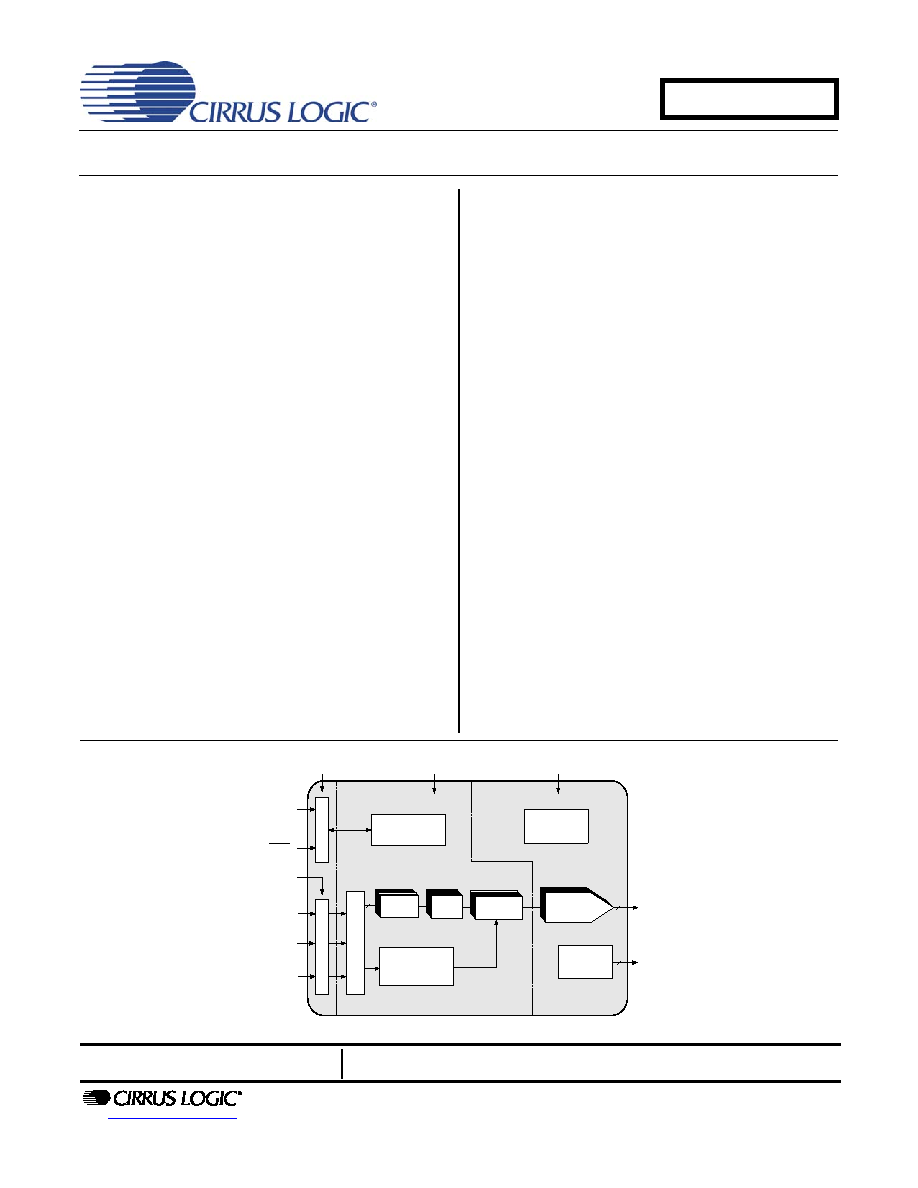
Description
The CS4364 is a complete 6-channel digital-to-analog
system. This D/A system includes digital de-emphasis,
half-dB step size volume control, ATAPI channel mix-
ing, selectable fast and slow digital interpolation filters
followed by an oversampled, multi-bit delta sigma mod-
ulator which includes mismatch shaping technology that
eliminates distortion due to capacitor mismatch. Follow-
ing this stage is a multi-element switched capacitor
stage and low-pass filter with single-ended analog
outputs.
The CS4364 also has a proprietary DSD processor
which allows for volume control and 50 kHz on-chip fil-
tering without an intermediate decimation stage. It also
offers an optional path for direct DSD conversion by di-
rectly using the multi-element switched capacitor array.
The CS4364 accepts PCM data at sample rates from
4 kHz to 216 kHz, DSD audio data, and delivers excel-
lent sound quality. These features are ideal for multi-
channel audio systems including SACD players, A/V re-
ceivers, digital TV's, mixing consoles, effects
processors, sound cards and automotive audio
systems.
This product is available in 48-pin LQFP package and is
available in both Automotive (-40∞ C - +85∞ C) and
Commercial (-10∞ C - +70∞ C) temperature grades. For
full Ordering Information see
page 49
.
Control Port Supply = 1.8 V to 5 V
Register/Hardware
Configuration
Internal Voltage
Reference
Reset
S
e
ri
a
l
In
te
rfa
c
e
L
e
v
e
l
T
r
an
s
l
at
or
L
e
vel
T
r
an
s
l
at
or
TDM Serial
Audio Input
Digital Supply = 2.5 V
Hardware Mode or
I
2
C/SPI Software Mode
Control Data
Analog Supply = 5 V
Six Channels of
Single-Ended
Outputs
6
PCM Serial
Audio Input
Volume
Controls
Digital
Filters
Switch-Cap
DAC and
Analog Filters
Multi-bit
Modulators
DSD Audio
Input
DSD Processor
-Volume control
-50 kHz filter
External Mute
Control
Mute Signals
6
6
Serial Audio Port
Supply = 1.8 V to 5 V
AUGUST '05
DS619A1
CS4364

2
DS619A1
CS4364
TABLE OF CONTENTS
1. PIN DESCRIPTION................................................................................................................................. 6
2. CHARACTERISTICS AND SPECIFICATIONS...................................................................................... 8
SPECIFIED OPERATING CONDITIONS .................................................................................................... 8
ABSOLUTE MAXIMUM RATINGS............................................................................................................... 8
DAC ANALOG CHARACTERISTICS........................................................................................................... 9
DAC ANALOG CHARACTERISTICS - ALL MODES (CONTINUED) ........................................................ 10
POWER AND THERMAL CHARACTERISTICS........................................................................................ 10
COMBINED INTERPOLATION & ON-CHIP ANALOG FILTER RESPONSE............................................ 11
COMBINED INTERPOLATION & ON-CHIP ANALOG FILTER RESPONSE............................................ 12
DSD COMBINED DIGITAL & ON-CHIP ANALOG FILTER RESPONSE .................................................. 12
DIGITAL CHARACTERISTICS .................................................................................................................. 13
SWITCHING CHARACTERISTICS - PCM ................................................................................................ 14
SWITCHING CHARACTERISTICS - DSD................................................................................................. 15
SWITCHING CHARACTERISTICS - CONTROL PORT - I≤C FORMAT.................................................... 16
SWITCHING CHARACTERISTICS - CONTROL PORT - SPITM FORMAT ............................................... 17
3. APPLICATIONS ................................................................................................................................... 20
3.1 Master Clock.................................................................................................................................. 20
3.2 Mode Select.................................................................................................................................. 21
3.3 Digital Interface Formats ............................................................................................................... 22
3.3.1 OLM #1 ................................................................................................................................ 23
3.3.2 OLM #2 ................................................................................................................................ 23
3.3.3 TDM ..................................................................................................................................... 24
3.4 Oversampling Modes..................................................................................................................... 24
3.5 Interpolation Filter.......................................................................................................................... 24
3.6 De-Emphasis ................................................................................................................................. 25
3.7 ATAPI Specification....................................................................................................................... 25
3.8 Direct Stream Digital (DSD) Mode................................................................................................. 26
3.9 Grounding and Power Supply Arrangements ................................................................................ 27
3.9.1 Capacitor Placement............................................................................................................ 27
3.10 Analog Output and Filtering......................................................................................................... 27
3.11 The MUTEC Outputs ................................................................................................................... 28
3.12 Recommended Power-Up Sequence .......................................................................................... 28
3.12.1 Hardware Mode.................................................................................................................. 28
3.12.2 Software Mode ................................................................................................................... 29
3.13 Recommended Procedure for Switching Operational Modes...................................................... 29
3.14 Control Port Interface .................................................................................................................. 29
3.14.1 MAP Auto Increment .......................................................................................................... 29
3.14.2 I≤C Mode ............................................................................................................................ 29
3.14.3 SPITM Mode........................................................................................................................ 31
3.15 Memory Address Pointer (MAP)................................................................................................. 31
3.15.1 INCR (Auto Map Increment Enable) .................................................................................. 31
3.15.2 MAP4-0 (Memory Address Pointer) ................................................................................... 31
4. REGISTER QUICK REFERENCE ....................................................................................................... 32
5. REGISTER DESCRIPTION .................................................................................................................. 32
5.1 Chip Revision (address 01h) ......................................................................................................... 33
5.1.1 Part Number ID (part) [Read Only]....................................................................................... 33
5.2 Mode Control 1 (address 02h) ....................................................................................................... 33
5.2.1 Control Port Enable (CPEN) ................................................................................................ 33
5.2.2 Freeze Controls (FREEZE) .................................................................................................. 33
5.2.3 PCM/DSD Selection (DSD/PCM)......................................................................................... 33
5.2.4 DAC Pair Disable (DACx_DIS) ............................................................................................ 34
5.2.5 Power Down (PDN).............................................................................................................. 34

DS619A1
3
CS4364
5.3 PCM Control (address 03h) ........................................................................................................... 34
5.3.1 Digital Interface Format (DIF)............................................................................................... 34
5.3.2 Functional Mode (FM) .......................................................................................................... 35
5.4 DSD Control (address 04h) ........................................................................................................... 35
5.4.1 DSD Mode Digital Interface Format (DSD_DIF) .................................................................. 35
5.4.2 Direct DSD Conversion (DIR_DSD)..................................................................................... 35
5.4.3 Static DSD Detect (STATIC_DSD) ...................................................................................... 36
5.4.4 Invalid DSD Detect (INVALID_DSD).................................................................................... 36
5.4.5 DSD Phase Modulation Mode Select (DSD_PM_MODE).................................................... 36
5.4.6 DSD Phase Modulation Mode Enable (DSD_PM_EN) ........................................................ 36
5.5 Filter Control (address 05h) ........................................................................................................... 36
5.5.1 Interpolation Filter Select (FILT_SEL).................................................................................. 36
5.6 Invert Control (address 06h) .......................................................................................................... 37
5.6.1 Invert Signal Polarity (INV_xx) ............................................................................................. 37
5.7 Group Control (address 07h) ......................................................................................................... 37
5.7.1 Mute Pin Control (MUTEC1, MUTEC0) ............................................................................... 37
5.7.2 Channel A Volume = Channel B Volume (Px_A=B)............................................................. 37
5.7.3 Single Volume Control (SNGLVOL) ..................................................................................... 38
5.8 Ramp and Mute (address 08h) ...................................................................................................... 38
5.8.1 Soft Ramp and Zero Cross Control (SZC) ........................................................................... 38
5.8.2 Soft Volume Ramp-Up After Error (RMP_UP) ..................................................................... 38
5.8.3 Soft Ramp-Down Before Filter Mode Change (RMP_DN) ................................................... 39
5.8.4 PCM Auto-Mute (PAMUTE) ................................................................................................. 39
5.8.5 DSD Auto-Mute (DAMUTE) ................................................................................................. 39
5.8.6 MUTE Polarity and DETECT (MUTEP1:0)........................................................................... 39
5.9 Mute Control (address 09h)........................................................................................................... 40
5.9.1 Mute (MUTE_xx) .................................................................................................................. 40
5.10 Mixing Control (address 0Ah, 0Dh, 10h, 13h).............................................................................. 40
5.10.1 De-Emphasis Control (PX_DEM1:0).................................................................................. 40
5.11 ATAPI Channel Mixing and Muting (ATAPI) ................................................................................ 41
5.12 Volume Control (address 0Bh, 0Ch, 0Eh, 0Fh, 11h, 12h) ........................................................... 42
5.12.1 Digital Volume Control (xx_VOL7:0) .................................................................................. 42
5.13 PCM Clock Mode (address 16h).................................................................................................. 42
5.13.1 Master Clock Divide by 2 Enable (MCLKDIV).................................................................... 42
6. FILTER RESPONSE PLOTS ............................................................................................................... 43
7. REFERENCES...................................................................................................................................... 47
8. PARAMETER DEFINITIONS................................................................................................................ 47
9. PACKAGE DIMENSIONS .................................................................................................................... 48
10. ORDERING INFORMATION .............................................................................................................. 49
11. REVISION HISTORY ......................................................................................................................... 49

4
DS619A1
CS4364
LIST OF FIGURES
Figure 1. Serial Audio Interface Timing...................................................................................................... 14
Figure 2. TDM Serial Audio Interface Timing ............................................................................................. 14
Figure 3. Direct Stream Digital - Serial Audio Input Timing........................................................................ 15
Figure 4. Direct Stream Digital - Serial Audio Input Timing for Phase Modulation Mode........................... 15
Figure 5. Control Port Timing - I≤C Format................................................................................................. 16
Figure 6. Control Port Timing - SPI Format................................................................................................ 17
Figure 7. Typical Connection Diagram, Software Mode............................................................................. 18
Figure 8. Typical Connection Diagram, Hardware Mode ........................................................................... 19
Figure 9. Format 0 - Left-Justified up to 24-bit Data .................................................................................. 22
Figure 10. Format 1 - I≤S up to 24-bit Data ................................................................................................ 22
Figure 11. Format 2 - Right-Justified 16-bit Data ....................................................................................... 22
Figure 12. Format 3 - Right-Justified 24-bit Data ....................................................................................... 22
Figure 13. Format 4 - Right-Justified 20-bit Data ....................................................................................... 22
Figure 14. Format 5 - Right-Justified 18-bit Data ....................................................................................... 23
Figure 15. Format 8 - One Line Mode 1..................................................................................................... 23
Figure 16. Format 9 - One Line Mode 2..................................................................................................... 23
Figure 17. Format 12 - TDM Mode............................................................................................................. 24
Figure 18. De-Emphasis Curve.................................................................................................................. 25
Figure 19. ATAPI Block Diagram (x = channel pair 1, 2, or 3) ................................................................... 25
Figure 20. DSD Phase Modulation Mode Diagram .................................................................................... 26
Figure 21. Full-Scale Output ...................................................................................................................... 27
Figure 22. Recommended Output Filter..................................................................................................... 27
Figure 23. Recommended Mute Circuitry .................................................................................................. 28
Figure 24. Control Port Timing, I≤C Mode .................................................................................................. 30
Figure 25. Control Port Timing, SPI Mode ................................................................................................. 31
Figure 26. Single-Speed (fast) Stopband Rejection................................................................................... 43
Figure 27. Single-Speed (fast) Transition Band ......................................................................................... 43
Figure 28. Single-Speed (fast) Transition Band (detail) ............................................................................. 43
Figure 29. Single-Speed (fast) Passband Ripple ....................................................................................... 43
Figure 30. Single-Speed (slow) Stopband Rejection ................................................................................. 43
Figure 31. Single-Speed (slow) Transition Band........................................................................................ 43
Figure 32. Single-Speed (slow) Transition Band (detail)............................................................................ 44
Figure 33. Single-Speed (slow) Passband Ripple...................................................................................... 44
Figure 34. Double-Speed (fast) Stopband Rejection ................................................................................. 44
Figure 35. Double-Speed (fast) Transition Band........................................................................................ 44
Figure 36. Double-Speed (fast) Transition Band (detail)............................................................................ 44
Figure 37. Double-Speed (fast) Passband Ripple...................................................................................... 44
Figure 38. Double-Speed (slow) Stopband Rejection ................................................................................ 45
Figure 39. Double-Speed (slow) Transition Band ...................................................................................... 45
Figure 40. Double-Speed (slow) Transition Band (detail) .......................................................................... 45
Figure 41. Double-Speed (slow) Passband Ripple .................................................................................... 45
Figure 42. Quad-Speed (fast) Stopband Rejection .................................................................................... 45
Figure 43. Quad-Speed (fast) Transition Band .......................................................................................... 45
Figure 44. Quad-Speed (fast) Transition Band (detail) .............................................................................. 46
Figure 45. Quad-Speed (fast) Passband Ripple ........................................................................................ 46
Figure 46. Quad-Speed (slow) Stopband Rejection................................................................................... 46
Figure 47. Quad-Speed (slow) Transition Band......................................................................................... 46
Figure 48. Quad-Speed (slow) Transition Band (detail)............................................................................. 46
Figure 49. Quad-Speed (slow) Passband Ripple....................................................................................... 46

DS619A1
5
CS4364
LIST OF TABLES
Table 1. Single-Speed Mode Standard Frequencies ................................................................................ 20
Table 2. Double-Speed Mode Standard Frequencies............................................................................... 20
Table 3. Quad-Speed Mode Standard Frequencies ................................................................................. 20
Table 4. PCM Digital Interface Format, Hardware Mode Options............................................................. 21
Table 5. Mode Selection, Hardware Mode Options .................................................................................. 21
Table 6. Direct Stream Digital (DSD), Hardware Mode Options ............................................................... 21
Table 7. Digital Interface Formats - PCM Mode........................................................................................ 34
Table 8. Digital Interface Formats - DSD Mode ........................................................................................ 35
Table 9. ATAPI Decode ............................................................................................................................ 41
Table 10. Example Digital Volume Settings .............................................................................................. 42