 | –≠–ª–µ–∫—Ç—Ä–æ–Ω–Ω—ã–π –∫–æ–º–ø–æ–Ω–µ–Ω—Ç: CS4390-KP | –°–∫–∞—á–∞—Ç—å:  PDF PDF  ZIP ZIP |

1
Copyright
©
Cirrus Logic, Inc. 1998
(All Rights Reserved)
Cirrus Logic, Inc.
Crystal Semiconductor Products Division
P.O. Box 17847, Austin, Texas 78760
(512) 445 7222 FAX: (512) 445 7581
http://www.crystal.com
CS4390
24-Bit, Stereo D/A Converter for Digital Audio
Features
l
24-Bit Conversion
l
115 dB Signal-to-Noise-Ratio (EIAJ)
l
Complete Stereo DAC System
-- 128X Interpolation Filter
-- Delta-Sigma DAC
-- Analog Post Filter
l
106 dB Dynamic Range
l
Low Clock Jitter Sensitivity
l
Filtered Line-Level Outputs
-- Linear Phase Filtering
-- Zero Phase Error Between Channels
l
Adjustable System Sampling Rates
-- including 32 kHz, 44.1 kHz & 48 kHz
l
Digital De-emphasis for 32 kHz, 44.1 kHz, &
48 kHz
l
Pin-compatible with the CS4329
Description
The CS4390 is a complete stereo digital-to-analog out-
put system. In addition to the traditional D/A function, the
CS4390 includes a digital interpolation filter followed by
an 128X oversampled delta-sigma modulator. The mod-
ulator output controls the reference voltage input to an
ultra-linear analog low-pass filter. This architecture al-
lows for infinite adjustment of sample rate between 1 and
50 kHz while maintaining linear phase response simply
by changing the master clock frequency.
The CS4390 also includes an extremely flexible serial
port utilizing mode select pins to support multiple inter-
face formats.
The master clock can be either 256, 384, or 512 times
the input sample rate, supporting various audio
environments.
ORDERING INFORMATION
CS4390-KP
-10∞ to 70∞ C
20-pin Plastic DIP
CS4390-KS
-10∞ to 70∞ C
20-pin Plastic SSOP
CDB4390
Evaluation Board
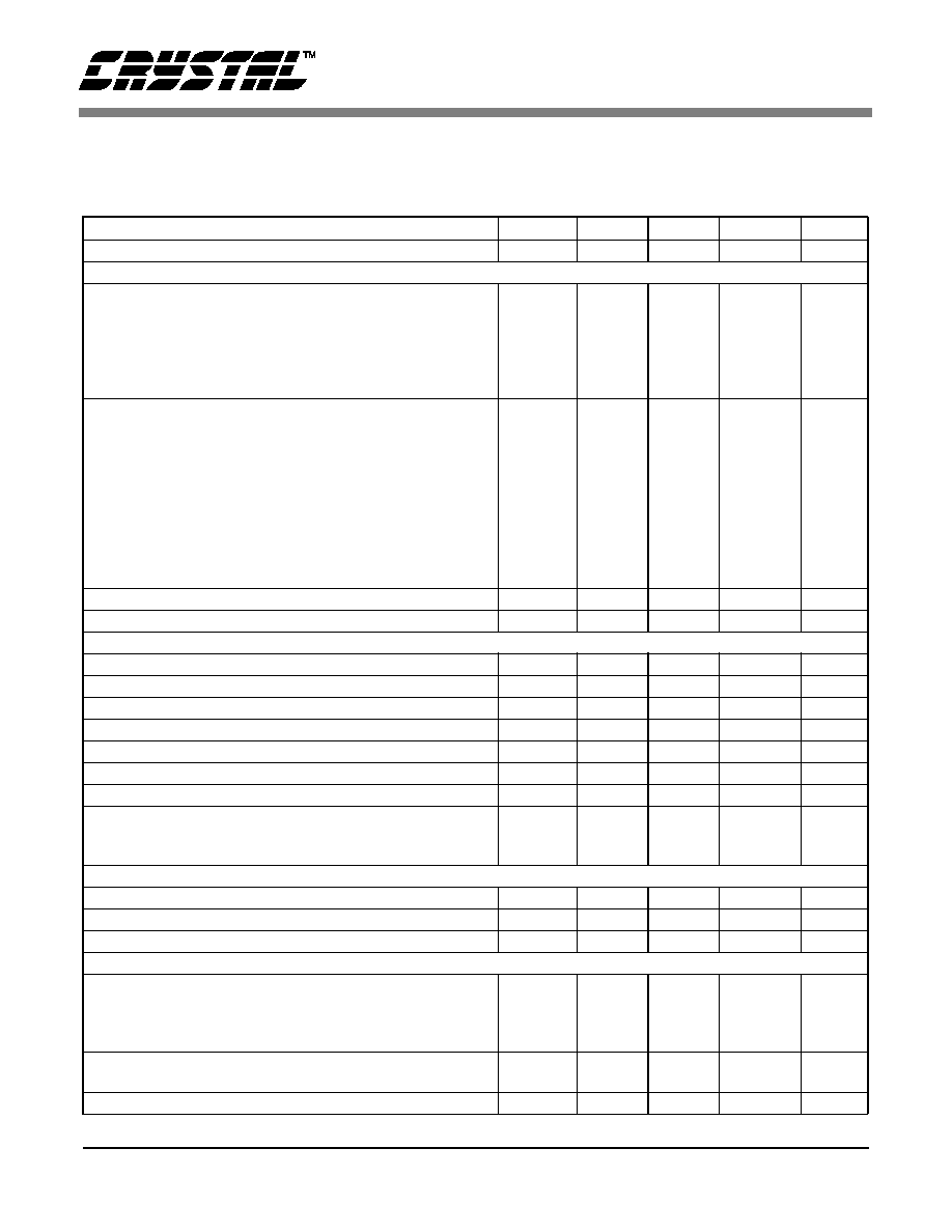
I
LRCK
AUTO_MUTE
DGND
DIF0
MUTE_L
20
16
5
11
7
SCLK
9
SDATA
10
DIF1
19
DEM0
1
DEM1
2
MCLK
8
AGND
4
VA
VD
AOUTL+
18
AOUTR+
14
Serial Input
Interface
Interpolator
Interpolator
De-emphasis
Delta-Sigma
Modulator
Delta-Sigma
Modulator
DAC
DAC
Voltage Reference
Analog
Low-Pass
Filter
Analog
Low-Pass
Filter
DIF2
12
3
6
AOUTL-
17
AOUTR-
13
MUTE_R
15
JUN `98
DS264F1
CS4390
2 DS264F1
ANALOG CHARACTERISTICS
(T
A
= 25∞C; Full-Scale Differential Output Sine wave, 997 Hz; Fs =
48 kHz; Input Data = 24 Bits; SCLK = 3.072 MHz; MCLK = 12.288 MHz; R
L
= 20 k
differential; VD = VA = 5 V;
Logic "1" = VD; Logic "0" = DGND; Measurement Bandwidth is 10 Hz to 20 kHz, unweighted unless otherwise
specified.)
Parameter Symbol Min Typ Max Unit
Specified Temperature Operating Range T
A
-10 - 70 ∞C
Dynamic Performance
Dynamic
Range 24-Bit (Note 1)
(A-Weighted)
20-Bit
(A-Weighted)
16-Bit
(A-Weighted)
98
101
-
-
-
-
103
106
103
106
94
96
-
-
-
-
-
-
dB
dB
dB
dB
dB
dB
Total Harmonic Distortion + Noise (Note 1)
24-Bit 0 dB
-20 dB
-60 dB
20-Bit 0 dB
-20 dB
-60 dB
16-Bit 0 dB
-20 dB
-60 dB
THD+N
-90
-78
-38
-
-
-
-
-
-
-98
-83
-43
-98
-83
-43
-93
-74
-34
-
-
-
-
-
-
-
-
-
dB
dB
dB
dB
dB
dB
dB
dB
dB
Idle Channel Noise / Signal-to-Noise-Ratio (Note 2) - 115 - dBFS
Interchannel Isolation (1 kHz) - -110 - dB
Combined Digital and Analog Filter Characteristics
Frequency Response 10 Hz to 20 kHz (Note 3) - ±0.1 - dB
Deviation from linear phase - ±0.5 - deg
Passband: to -0.1 dB corner (Note 3) 0 - 21.77 kHz
Passband Ripple - - ±0.001 dB
StopBand (Note 3) 26.23 - - kHz
StopBand Attenuation (Note 3) 75 - - dB
Group Delay (Note 4) - 25/Fs - s
De-emphasis Error (referenced to 1 kHz) Fs = 32 kHz
Fs = 44.1 kHz
Fs = 48 kHz
-
-
-
-
-
-
+0.3/-0.3
+0.2/-0.4
+0.1/-0.45
dB
dB
dB
dc Accuracy
Interchannel Gain Mismatch - 0.1 - dB
Gain Error - ±2 ±5 %
Gain Drift - 200 - ppm/∞C
Power Supplies
Power Supply Current: Normal Operation
Power-down
I
A
I
D
I
A
+I
D
-
-
-
-
30
12
42
500
-
-
45
-
mA
mA
mA
µ
A
Power Dissipation Normal Operation
Power-down
-
-
210
2.5
225
-
mW
mW
Power Supply Rejection Ratio (1 kHz) PSRR - 60 - dB
CS4390
DS264F1 3
ANALOG CHARACTERISTICS (CONTINUED)
Notes: 1. Triangular PDF Dithered Data
2. AUTO-MUTE active. See parameter definitions
3. The passband and stopband edges scale with frequency. For input sample rates, Fs, other than 48 kHz,
the passband edge is 0.4535◊Fs and the stopband edge is 0.5465◊Fs.
4. Group Delay for Fs=48 kHz 25/48 kHz=520
µ
s
5. Specified for a fully differential output ±((AOUT+)-(AOUT-)). See Figure 12.
SWITCHING CHARACTERISTICS
(T
A
= -10 to 70∞C; Logic 0 = AGND = DGND; Logic
1 = VD = VA = 5.25 to 4.75 Volts; C
L
= 20 pF)
Parameter Symbol Min Typ Max Unit
Analog Output
Differential Full Scale Output
Voltage
(Note 5) 1.90 2.0 2.10 Vrms
Output Common Mode Voltage - 2.2 - V
Differential Offset - 3 15 mV
AC Load Resistance R
L
4
-
-
k
Load Capacitance C
L
- - 100 pf
Parameter Symbol Min Typ Max Unit
Input Sample Rate Fs 1 - 50 kHz
MCLK Pulse Width High MCLK / LRCK = 512 10 - - ns
MCLK Pulse Width Low MCLK / LRCK = 512 10 - - ns
MCLK Pulse Width High MCLK / LRCK = 384 21 - - ns
MCLK Pulse Width Low MCLK / LRCK = 384 21 - - ns
MCLK Pulse Width High MCLK / LRCK = 256 31 - - ns
MCLK Pulse Width Low MCLK / LRCK = 256 32 - - ns
External SCLK Mode
SCLK Pulse Width Low t
sclkl
20
-
-
ns
SCLK Pulse Width High t
sclkh
20
-
-
ns
SCLK Period t
sclkw
-
-
ns
SCLK rising to LRCK edge delay t
slrd
20
-
-
ns
SCLK rising to LRCK edge setup time t
slrs
20
-
-
ns
SDATA valid to SCLK rising setup time t
sdlrs
20
-
-
ns
SCLK rising to SDATA hold time t
sdh
20
-
-
ns
Internal SCLK Mode
SCLK Period SCLK / LRCK = 64 t
sclkw
-
-
ns
SDATA valid to SCLK rising setup time t
sdlrs
-
-
ns
SCLK rising to SDATA hold time MCLK / LRCK = 256 or
512
t
sdh
-
-
ns
SCLK rising to SDATA hold time MCLK / LRCK = 384 t
sdh
-
-
ns
1
128 Fs
( )
--------------------
1
64 Fs
( )
-----------------
1
512 Fs
( )
-------------------- 10
+
1
512 Fs
( )
-------------------- 15
+
1
384 Fs
( )
-------------------- 15
+
CS4390
4
DS264F1
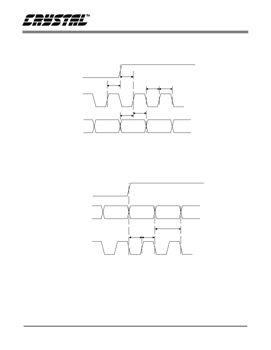
sclkh
t
slrs
t
slrd
t
sdlrs
t
sdh
t
sclkl
t
SDATA
SCLK
LRCK
SDATA
*INTERNAL SCLK
LRCK
sclkw
t
sdlrs
t
sdh
t
External Serial Mode Input Timing
Internal Serial Mode Input Timing
* The SCLK pin must be terminated to ground.
The SCLK pulses shown are internal to the CS4390.

CS4390
DS264F1
5
DIGITAL CHARACTERISTICS
(T
A
= 25∞C; VD = 5 V ±5%)
ABSOLUTE MAXIMUM RATINGS
(AGND = 0 V, all voltages with respect to ground.)
WARNING: Operation at or beyond these limits may result in permanent damage to the device. Normal operation
is not guaranteed at these extremes.
RECOMMENDED OPERATING CONDITIONS
(DGND = 0V; all voltages with respect to ground)
Parameter
Symbol Min Typ
Max
Unit
High-Level Input Voltage
V
IH
2.0
-
-
V
Low-Level Input Voltage
V
IL
-
-
0.8
V
Input Leakage Current
V
in
-
-
±10.0
µ
A
Digital Input Capacitance
-
10
-
pF
Parameter
Symbol Min
Max
Unit
DC Power Supply:
Positive Analog
Positive Digital
|VA - VD|
VA
VD
-0.3
-0.3
0.0
6.0
6.0
0.4
V
V
V
Input Current, Any Pin Except Supplies
I
in
-
±10
mA
Digital Input Voltage
V
IND
-0.3
(VD)+0.4
V
Ambient Operating Temperature (power applied)
T
A
-55
125
∞C
Storage Temperature
T
stg
-65
150
∞C
Parameter
Symbol Min Typ
Max
Unit
DC Power Supply:
Positive Digital
Positive Analog
|VA - VD|
VD
VA
4.75
4.75
-
5.0
5.0
-
5.25
5.25
0.4
V
V
V