 | –≠–ª–µ–∫—Ç—Ä–æ–Ω–Ω—ã–π –∫–æ–º–ø–æ–Ω–µ–Ω—Ç: CS44210 | –°–∫–∞—á–∞—Ç—å:  PDF PDF  ZIP ZIP |
Advance Product Information
This document contains information for a new product.
Cirrus Logic reserves the right to modify this product without notice.
1
Copyright
Cirrus Logic, Inc. 2001
(All Rights Reserved)
P.O. Box 17847, Austin, Texas 78760
(512) 445 7222 FAX: (512) 445 7581
http://www.cirrus.com
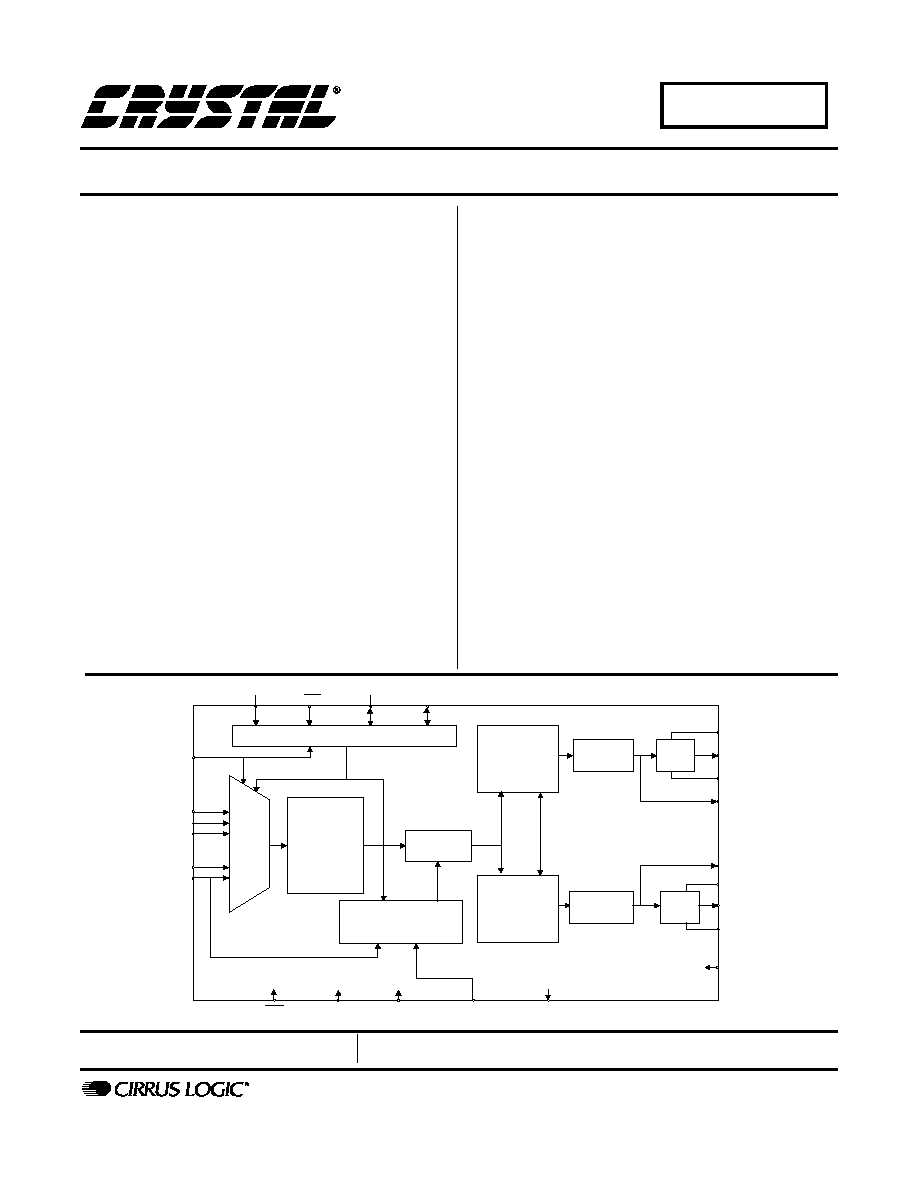
CS44210
Digital PWM Controller with Headphone Monitor
Features
l
Up
to 100 dB Dynamic Range
l
2.4 V to 5.0 V supply
l
Sample rates up to 96 kHz
l
Digital Tone Control
--3 selectable HPF and LPF corner frequencies
--12 dB boost for bass and treble - 1 dB step size
l
Programmable Digital volume control
--+18 to -96 dB in 1 dB steps
l
Peak signal soft limiting
l
De-emphasis for 32 kHz, 44.1 kHz, and 48
kHz
l
Selectable outputs for each channel including
--Channel A: R, L, mono (L + R) / 2, mute
--Channel B: R, L, mono (L + R) / 2, mute
l
PWM PopGuard
Æ
Description
The CS44210 is a complete stereo digital-to-PWM Class D au-
dio amplifier system controller including interpolation, volume
control, half bridge PWM driver outputs, and an integrated
CS44L10 headphone amplifier in a 24-pin TSSOP package.
The CS44210 architecture uses a direct-to-digital approach
that maintains digital signal integrity to the final output filter.
This minimizes analog interference effects that can negatively
affect system performance.
The CS44210 contains on-chip digital bass and treble boost,
peak signal limiting, and de-emphasis. The PWM amplifier can
achieve greater than 90% efficiency. This efficiency leads to
longer battery life for portable systems, smaller device pack-
age, less heat sink requirements, and smaller power supplies.
The CS44210 provides all the controls necessary to drive high-
er voltage output stages for increased power levels.
The CS44210 is ideal for integrated, mult-function systems
such as shelf-top audio systems, audio mini systems, audio
video receivers (AVR), boom boxes and powered speakers.
ORDERING INFORMATION
CS44210-KZ -10 to 70 ∞C 24-pin TSSOP
Multibit
Modulator with
Correction
Multibit
Modulator with
Correction
Digital V olume
Control,
Bass/Treble
Boost,
Compression
Limiting,
De-emphasis
Control Port
SCL/CCLK/DIF0
MCLK
Input
MUX
and
Serial
Port
SDA/CDIN/DEM
VL
PW M
Conversion
PW M
Conversion
SYNC_CLK
DRIV ER_B
HP_B
VA_HPB
GND_HPB
Level
Shifter
VA_HPA
Level
Shifter
HP_A
GND_HPA
RST
Interpolation
AD1/CDOUT
TSTIN
SCLK
LRCK
Input Sampling Rate
LRCLK/MCLK Ratio
AD0/CS/DIF1
SDIN1
SDIN2
SDIN3
DRIVER_A
VD
GND
MAY `01
DS539PP1

CS44210
2
DS539PP1
TABLE OF CONTENTS
1. CHARACTERISTICS AND SPECIFICATIONS ........................................................................ 4
2. TYPICAL CONNECTION DIAGRAM ...................................................................................... 11
3. REGISTER QUICK REFERENCE ...................................................................................... 13
4. REGISTER DESCRIPTIONS .................................................................................................. 14
5. PIN DESCRIPTION ................................................................................................................. 27
6. APPLICATIONS ..................................................................................................................... 29
6.1 Grounding and Power Supply Decoupling ...................................................................... 29
6.2 Clock Modes ................................................................................................................... 29
6.3 De-Emphasis .................................................................................................................. 29
6.4 PWM PopGuard Transient Control ................................................................................. 29
6.5 Recommended Power-up Sequence .............................................................................. 30
6.5.1 Stand Alone Mode ................................................................................................ 30
6.5.2 Control Port Mode ................................................................................................ 30
7. CONTROL PORT INTERFACE .............................................................................................. 31
7.1 Format Selection ............................................................................................................. 31
7.2 Two-Wire Format ............................................................................................................ 31
7.2.1 Writing in Two-Wire Format ................................................................................. 31
7.2.2 Reading in Two-Wire Format ............................................................................... 31
7.3 SPI Format ...................................................................................................................... 31
7.3.1 Writing in SPI ....................................................................................................... 31
7.3.2 Reading in SPI ..................................................................................................... 33
7.4 Memory Address Pointer (MAP) ................................................................................... 33
7.4.1 INCR (Auto Map Increment Enable) .................................................................... 33
7.4.2 MAP3-0 (Memory Address Pointer) ..................................................................... 33
8. PARAMETER DEFINITIONS .................................................................................................. 36
9. PACKAGE DIMENSIONS ....................................................................................................... 37
LIST OF FIGURES
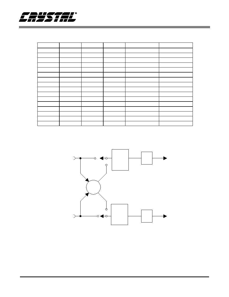
Figure 1. Serial Audio Data Interface Timing .................................................................................. 7
Figure 2. Control Port Timing - Two-Wire Format ........................................................................... 9
Figure 3. Control Port Timing - SPI Format ................................................................................... 10
Figure 4. Typical CS44210 Connection Diagram Stand-Alone Mode ........................................... 11
Figure 5. Typical CS44210 Connection Diagram Control Port Mode ............................................ 12
Figure 6. Dynamics Control Block Diagram .................................................................................. 21
Figure 7. De-Emphasis Curve ....................................................................................................... 24
Figure 8. Control Port Timing, Two-Wire Format .......................................................................... 32
Contacting Cirrus Logic Support
For a complete listing of Direct Sales, Distributor, and Sales Representative contacts, visit the Cirrus Logic web site at:
http://www.cirrus.com/corporate/contacts/sales.cfm
Preliminary product information describes products which are in production, but for which full characterization data is not yet available. Advance product infor-
mation describes products which are in development and subject to development changes. Cirrus Logic, Inc. has made best efforts to ensure that the information
contained in this document is accurate and reliable. However, the information is subject to change without notice and is provided "AS IS" without warranty of
any kind (express or implied). Customers are advised to obtain the latest version of relevant information to verify, before placing orders, that information being
relied on is current and complete. All products are sold subject to the terms and conditions of sale supplied at the time of order acknowledgment, including those
pertaining to warranty, patent infringement, and limitation of liability. No responsibility is assumed by Cirrus Logic, Inc. for the use of this information, including
use of this information as the basis for manufacture or sale of any items, nor for infringements of patents or other rights of third parties. This document is the
property of Cirrus Logic, Inc. and by furnishing this information, Cirrus Logic, Inc. grants no license, express or implied under any patents, mask work rights,
copyrights, trademarks, trade secrets or other intellectual property rights of Cirrus Logic, Inc. Cirrus Logic, Inc., copyright owner of the information contained
herein, gives consent for copies to be made of the information only for use within your organization with respect to Cirrus Logic integrated circuits or other parts
of Cirrus Logic, Inc. The same consent is given for similar information contained on any Cirrus Logic website or disk. This consent does not extend to other
copying such as copying for general distribution, advertising or promotional purposes, or for creating any work for resale. The names of products of Cirrus Logic,
Inc. or other vendors and suppliers appearing in this document may be trademarks or service marks of their respective owners which may be registered in some
jurisdictions. A list of Cirrus Logic, Inc. trademarks and service marks can be found at
http://www.cirrus.com
.

CS44210
DS539PP1
3
Figure 9. Control Port Timing, SPI Format (Write) ........................................................................ 32
Figure 10. Control Port Timing, SPI Format (Read)...................................................................... 33
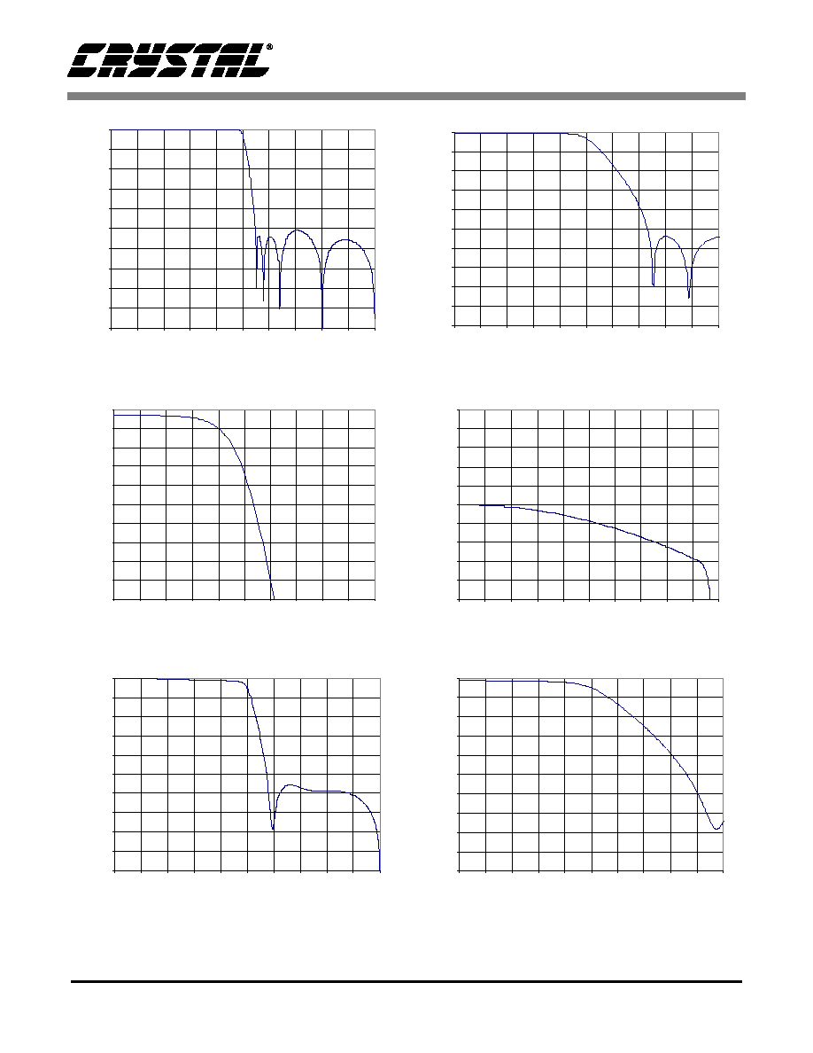
Figure 11. Single Speed Stopband Rejection ............................................................................... 34
Figure 12. Single Speed Transition Band ..................................................................................... 34
Figure 13. Single Speed Transition Band (Detail)......................................................................... 34
Figure 14. Single Speed Passband Ripple ................................................................................... 34
Figure 15. Double Speed Stopband Rejection.............................................................................. 34
Figure 16. Double Speed Transition Band .................................................................................... 34
Figure 17. Double Speed Transition Band (Detail) ....................................................................... 35
Figure 18. Double Speed Passband Ripple .................................................................................. 35
Figure 19. Left Justified, up to 24-Bit Data.................................................................................... 35
Figure 20. Right Justified, 24-Bit Data ......................................................................................... 35
Figure 21. I2S, Up to 24-Bit Data ................................................................................................. 35
Figure 22. Right Justified, 16-Bit Data .......................................................................................... 36
LIST OF TABLES
Table 1. Register Quick Reference .............................................................................................. 13
Table 2. Example Volume Settings .............................................................................................. 16
Table 3. Example Bass Boost Settings ........................................................................................ 16
Table 4. Example Treble Boost Settings ...................................................................................... 16
Table 5. Base Boost Corner Frequencies in Single Speed Mode ................................................ 17
Table 6. Base Boost Corner Frequencies in Double Speed Mode .............................................. 17
Table 7. Treble Boost Corner Frequencies in Single Speed Mode .............................................. 18
Table 8. Example Limiter Attack Rate Settings ............................................................................ 19
Table 9. Example Limiter Release Rate Settings ......................................................................... 19
Table 10. ATAPI Decode ............................................................................................................. 21
Table 11. Single Speed Clock Modes - Control Port Mode .......................................................... 23
Table 12. Single Speed Clock Modes - Stand-Alone Mode ......................................................... 23
Table 13. Double Speed Clock Modes - Control Port Mode ........................................................ 24
Table 14. Double Speed Clock Modes - Stand-Alone Mode ........................................................ 24
Table 15. Digital Interface Format - DIF1 and DIF0 (Stand-Alone Mode) .................................... 28
CS44210
4
DS539PP1
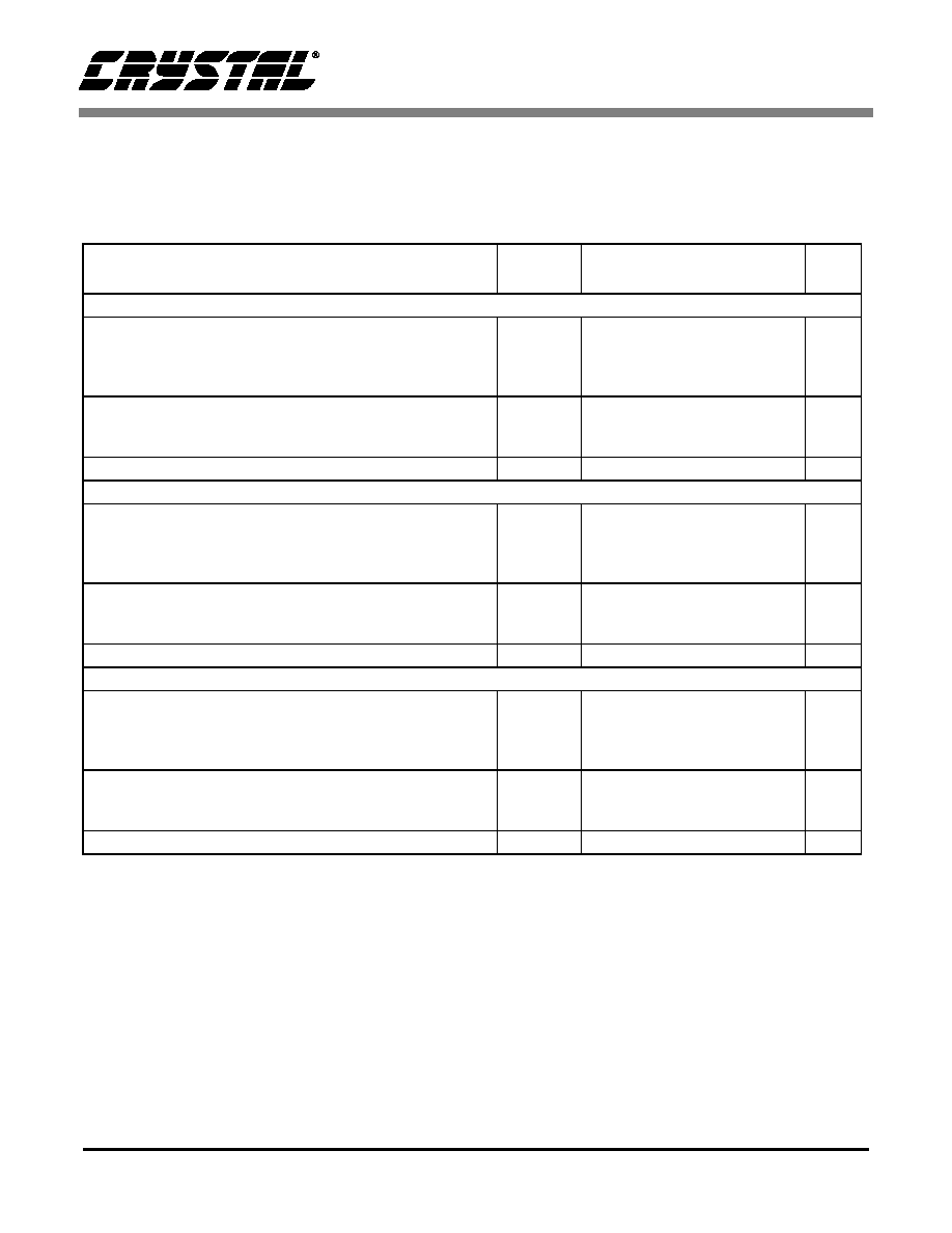
1. CHARACTERISTICS AND SPECIFICATIONS
(T
A
= 25 ∞C; GND = 0 V; Logic "1" = VL = 2.4 V; Logic "0" = GND = 0 V; Full-Scale Output Sine Wave, 997 Hz,
MCLK = 12.288 MHz, Measurement Bandwidth 10 Hz to 20 kHz, unless otherwise specified; Fs for Single Speed
Mode = 48 kHz, SCLK = 3.072 MHz; Fs for Double Speed Mode = 96 kHz, SCLK = 6.144 MHz. Test load
R
L
= 16
, C
L
= 10pF.) (See Typical CS44210 Connection Diagram.)
Parameter
Symbol
Min
Typ
Max
Unit
Headphone Output Dynamic Performance for VD = VL = VA_HPx = 2.4 V
Dynamic Range
18 to 24-Bit
A-Weighted
UnWeighted
16-Bit
A-Weighted
Unweighted
TBD
TBD
-
-
93
91
91
89
-
-
-
-
dB
dB
dB
dB
Total Harmonic Distortion + Noise
0 dBFS
-20 dBFS
-60 dBFS
THD+N
-
-
-
-62
-71
-31
TBD
-
-
dB
dB
dB
Interchannel Isolation
(1 kHz)
-
TBD
-
dB
Headphone Output Dynamic Performance for VD = VL = VA_HPx = 3.0 V
Dynamic Range
18 to 24-Bit
A-Weighted
UnWeighted
16-Bit
A-Weighted
Unweighted
TBD
TBD
-
-
95
92
92
90
-
-
-
-
dB
dB
dB
dB
Total Harmonic Distortion + Noise
0 dB
-20 dB
-60 dB
THD+N
-
-
-
-64
-72
-32
TBD
-
-
dB
dB
dB
Interchannel Isolation
(1 kHz)
-
TBD
-
dB
Headphone Output Dynamic Performance for VD = VL = VA_HPx = 5.0 V
Dynamic Range
18 to 24-Bit
A-Weighted
UnWeighted
16-Bit
A-Weighted
Unweighted
TBD
TBD
-
-
99
96
91
93
-
-
-
-
dB
dB
dB
dB
Total Harmonic Distortion + Noise
0 dB
-20 dB
-60 dB
THD+N
-
-
-
-67
-76
-36
TBD
-
-
dB
dB
dB
Interchannel Isolation
(1 kHz)
-
TBD
-
dB
CS44210
DS539PP1
5
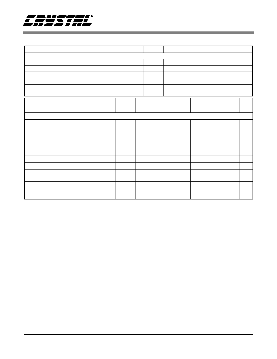
CHARACTERISTICS AND SPECIFICATIONS
(Continued)
Note:
1. Filter response is not tested but is guaranteed by design.
2. Response is clock dependent and will scale with Fs. Note that the response plots (Figures 11-18) have
been normalized to Fs and can be de-normalized by multiplying the X-axis scale by Fs.
3. Referenced to a 1 kHz, full-scale sine wave.
4. For Single Speed Mode, the measurement bandwidth is 0.5465 Fs to 3 Fs.
For Double Speed Mode, the measurement bandwidth is 0.577 Fs to 1.4 Fs.
5. De-emphasis is not available in double speed mode.
Parameters
Symbol
Min
Typ
Max
Units
PWM Headphone Output
Full Scale Headphone Output Voltage
TBD
0.85 x VA_HP
TBD
Vp
Headphone Output Quiescent Voltage
-
0.5 x VA_HP
-
VDC
Interchannel Gain Mismatch
-
0.1
-
dB
Modulation Index
-
-
85
%
Maximum Headphone Output
VA_HPx=2.4V
AC-Current
VA_HPx=5.0V
I
HP
-
-
45
80
-
-
mA
mA
Parameter
Single Speed Mode
Double Speed Mode
Symbol
Min
Typ
Max
Min
Typ
Max
Unit
Digital Filter Response (Note 1)
Passband
to -0.05 dB corner
(Note 2)
to -0.1 dB corner
to -3 dB corner
0
-
0
-
-
-
.4535
-
.4998
-
0
0
-
-
-
-
.4426
.4984
Fs
Fs
Fs
Frequency Response 10 Hz to 20 kHz
(Note 3)
-.02
-
+.08
0
-
+0.11
dB
StopBand
.5465
-
-
.577
-
-
Fs
StopBand Attenuation
(Note 4)
50
-
-
55
-
-
dB
Group Delay
tgd
-
9/Fs
-
-
4/Fs
-
s
Passband Group Delay Deviation
0 - 40 kHz
0 - 20 kHz
-
-
-
±0.36/Fs
-
-
-
-
±1.39/Fs
±0.23/Fs
-
-
s
s
De-emphasis Error
Fs = 32 kHz
(Relative to 1 kHz)
Fs = 44.1 kHz
Fs = 48 kHz
-
-
-
-
-
-
+.2/-.1
+.05/-.14
+0/-.22
(Note 5)
dB
dB
dB
CS44210
6
DS539PP1
ABSOLUTE MAXIMUM RATINGS
(GND = 0V; all voltages with respect to ground.)
CAUTION: Operation at or beyond these limits may result in permanent damage to the device. Normal operation
is not guaranteed at these extremes.
RECOMMENDED OPERATING CONDITIONS
(GND = 0V; all voltages with respect to ground.)
SWITCHING CHARACTERISTICS
(T
A
= -10 to 70∞C; VL = 2.4V - 5.0V; Inputs: Logic 0 = GND,
Logic 1 = VL, CL = 20pF)
Parameters
Symbol
Min
Max
Units
DC Power Supplies:
Headphone
Interface
Digital
VA_HPx
VL
VD
2.4
2.4
2.4
5.5
5.5
5.5
V
V
V
Input Current, Any Pin Except Supplies
I
in
±10
mA
Digital Input Voltage
V
IND
-0.3
VL + 0.4
V
Ambient Operating Temperature (power applied)
T
A
-55
125
∞C
Storage Temperature
T
stg
-65
150
∞C
Parameters
Symbol Min Typ
Max
Units
Ambient Temperature
T
A
-10
-
70
∞C
DC Power Supplies:
Headphone
Interface
Digital
VA_HPx
VL
VD
2.4
2.4
2.4
-
-
-
5.0
5.0
5.0
V
V
V
Parameters
Symbol Min Typ
Max
Units
Input Sample Rate
Single Speed Mode
Double Speed Mode
Fs
Fs
8
50
-
-
50
100
kHz
kHz
MCLK Duty Cycle
40
50
60
%
LRCK Duty Cycle
40
50
60
%
SCLK Pulse Width Low
t
sclkl
20
-
-
ns
SCLK Pulse Width High
t
sclkh
20
-
-
ns
SCLK Period
Single Speed Mode
t
sclkw
-
-
ns
Double Speed Mode
t
sclkw
-
-
ns
SCLK rising to LRCK edge delay
t
slrd
20
-
-
ns
SCLK rising to LRCK edge setup time
t
slrs
20
-
-
ns
SDIN valid to SCLK rising setup time
t
sdlrs
20
-
-
ns
SCLK rising to SDIN hold time
t
sdh
20
-
-
ns
1
128
(
)Fs
----------------------
1
64
( )Fs
-------------------

CS44210
DS539PP1
7
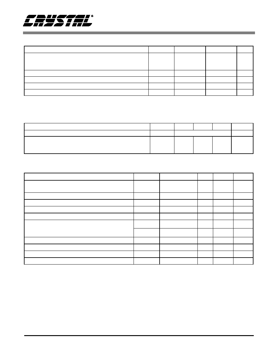
POWER AND THERMAL CHARACTERISTICS
(GND = 0 V; All voltages with respect to
ground. All measurements taken with all zeros input and open outputs, unless otherwise specified.)
Note:
6. Power Down Mode is defined as RST = LO with all clocks and data lines held static.
Parameters
Symbol
Min
Typ
Max
Units
Power Supplies
Power Supply Current-
VA_HPx= 2.4 V
Normal Operation
VD = 2.4 V
VL= 2.4 V
I
VA_HP
I
D
I
L
-
-
-
1
10
1
-
-
-
mA
mA
mA
Power Supply Current-
VA_HPx = 2.4V
Power Down Mode (Note 6)
VD = 2.4V
VL = 2.4V
I
VA_HP
I
D
I
L
-
-
-
TBD
TBD
TBD
-
-
-
µA
µA
µA
Power Supply Current-
VA_HPx = 5.0 V
Normal Operation
VD = 5.0 V
VL = 5.0 V
I
VA_HP
I
D
I
L
-
-
-
2
20
2
-
-
-
mA
mA
mA
Power Supply Current-
VA_HPx = 5.0V
Power Down Mode (Note 6)
VD = 5.0V
VL = 5.0 V
I
VA_HP
I
D
I
L
-
-
-
TBD
TBD
TBD
-
-
-
µA
µA
µA
Total Power Dissipation-
All Supplies = 2.4 V
Normal Operation
All Supplies = 5.0 V
-
-
29
120
-
-
mW
mW
Power Supply Rejection Ratio
PSRR
-
0
-
dB
Maximum Headphone Power Dissipation
VA=2.4 V
(1 kHz full-scale sine wave into 16 ohm load)
VA=5.0 V
-
-
23
100
-
-
mW
mW
Package Thermal Resistance
JA
-
75
-
∞C/Watt
sclkh
t
slrs
t
slrd
t
sdlrs
t
sdh
t
sclkl
t
SDATA
SCLK
LRCK
sclkw
t
Figure 1. Serial Audio Data Interface Timing
CS44210
8
DS539PP1
DIGITAL CHARACTERISTICS
(T
A
= 25∞ C; VL = 2.4 V - 3.6 V; GND = 0 V)
SWITCHING CHARACTERISTICS- CONTROL PORT- TWO-WIRE FORMAT
(Note 8) (T
A
= 25∞ C; VL = 2.4 V - 5.0 V; Inputs: Logic 0 = GND, Logic 1 = VL, C
L
= 30 pF)
Note:
7. V
OH
and V
OL
are tested at an output current of TBD mA.
8. The Two-Wire Format is compatible with the I
2
C protocol.
9. Data must be held for sufficient time to bridge the transition time, t
fc
, of SCL.
10. The acknowledge delay is based on MCLK and can limit the maximum transaction speed.
11.
for Single-Speed Mode and
for Double-Speed Mode.
Parameters
Symbol Min
Typ
Max
Units
High-Level Input Voltage
V
IH
0.7 x VL
-
-
V
Low-Level Input Voltage
V
IL
-
-
0.3 x VL
V
Input Leakage Current
I
in
-
-
±10
µA
Input Capacitance
-
8
-
pF
High-Level Output Voltage (Pin 15)
(Note 7)
V
OH
0.7 x VL
-
-
V
Low-Level Output Voltage (Pin 15)
(Note 7)
V
OL
-
-
0.3 x VL
V
High-Level Output Voltage (Pins 11, 13, 14)
(Note 7)
V
OH
0.7 x VD
-
-
V
Low-Level Output Voltage (Pins 11, 13, 14)
(Note 7)
V
OL
-
-
0.3 x VD
V
Parameter
Symbol
Min
Max
Unit
SCL Clock Frequency
f
scl
-
100
kHz
RST Rising Edge to Start
t
irs
500
-
ns
Bus Free Time Between Transmissions
t
buf
4.7
-
µs
Start Condition Hold Time (prior to first clock pulse)
t
hdst
4.0
-
µs
Clock Low time
t
low
4.7
-
µs
Clock High Time
t
high
4.0
-
µs
Setup Time for Repeated Start Condition
t
sust
4.7
-
µs
SDA Hold Time from SCL Falling
(Note 9)
t
hdd
0
-
µs
SDA Setup time to SCL Rising
t
sud
250
-
ns
Rise Time of SCL and SDA
t
rc
, t
rc
-
1
µs
Fall Time SCL and SDA
t
fc
, t
fc
-
300
ns
Setup Time for Stop Condition
t
susp
4.7
-
µs
Acknowledge Delay from SCL Falling
(Note 10)
t
ack
-
(Note 11)
ns
5
256
Fs
◊
---------------------
5
128
F s
◊
---------------------

CS44210
DS539PP1
9
t
buf
t
hdst
t
lo w
t
hdd
t
high
t
sud
Stop
St a rt
S D A
S C L
t
irs
R S T
t
hdst
t
rc
t fc
t sust
t susp
Sta rt
Stop
R e p e a te d
t rd
t fd
t
ack
Figure 2. Control Port Timing - Two-Wire Format

CS44210
10
DS539PP1
SWITCHING CHARACTERISTICS - CONTROL PORT - SPI FORMAT
(T
A
= 25∞ C; VL = 2.4 V - 5.0 V; Inputs: Logic 0 = GND, Logic 1 = VL, C
L
= 30 pF)
Note:
12. t
spi
only needed before first falling edge of CS after RST rising edge. t
spi
= 0 at all other times.
13. Data must be held for sufficient time to bridge the transition time of CCLK.
14. For F
SCK
< 1 MHz.
15. CDOUT should not be sampled during this time period.
16. This time is not tested but is guaranteed by design.
Parameter
Symbol
Min
Max
Unit
CCLK Clock Frequency
f
sclk
-
6
MHz
RST Rising Edge to CS Falling
t
srs
500
-
ns
CCLK Edge to CS Falling
(Note 12)
t
spi
500
-
ns
CS High Time Between Transmissions
t
csh
1.0
-
µs
CS Falling to CCLK Edge
t
css
20
-
ns
CCLK Low Time
t
scl
66
-
ns
CCLK High Time
t
sch
66
-
ns
CDIN to CCLK Rising Setup Time
t
dsu
40
-
ns
CCLK Rising to DATA Hold Time
(Note 13)
t
dh
15
-
ns
Rise Time of CCLK and CDIN
(Note 14)
t
r2
-
100
ns
Fall Time of CCLK and CDIN
(Note 15)
t
f2
-
100
ns
Transition time from CCLK to CDOUT valid
(Note 15)
t
scdov
-
40
ns
Time from CS rising to CDOUT high-Z
(Note 16)
t
cscdo
-
20
ns
t r2
t f2
t dsu t dh
t sch
t scl
CS
CCLK
CDIN
t css
t csh
t spi
t srs
RST
CDOUT
t scdov
t scdov
t cscdo
Tri-state
Figure 3. Control Port Timing - SPI Format

CS44210
DS539PP1
11
2. TYPICAL CONNECTION DIAGRAMS
MCLK
LRCK
SC LK
SDIN1
RST
VA_HPB
CS44210
2.4 to 5.0 V
Supply
100 µF
+
VA_HPA
Supply
1.0 µF
+
VL
19
20
8
7
2
5
3
18
21
16
1
9
4
15
14
2.4 to 5.0 V
Supply
1.0 µF
+
VD
6
2.4 to 5.0 V
24
SDIN2
SDIN3
AD1/CDOUT
2 3
10
DRIVER_A
17
22
0.15
µF
0.15
µF
16
Headphones
GND
GND
GND
0.1 µF
Digital
Audio
Source
DIF
DIF 0
1
DEM
0.1 µF
0.1 µ F
Mode
Control
HP_A
HP_B
TSTIN
12
11
SYNC_CLK
Sync Clock
13
DRIVER_B
Output
Filter
Output
Filter
220 µF
100 µH
220 µF
100 µH
Cout
+
+
Cout
MOSFET
Driver
&
Power
Stage
MOSFET
Driver
&
Power
Stage
*
*
* This feature is unavailable in this mode.
This pin should be grounded.
Figure 4. Typical CS44210 Connection Diagram Stand-Alone Mode
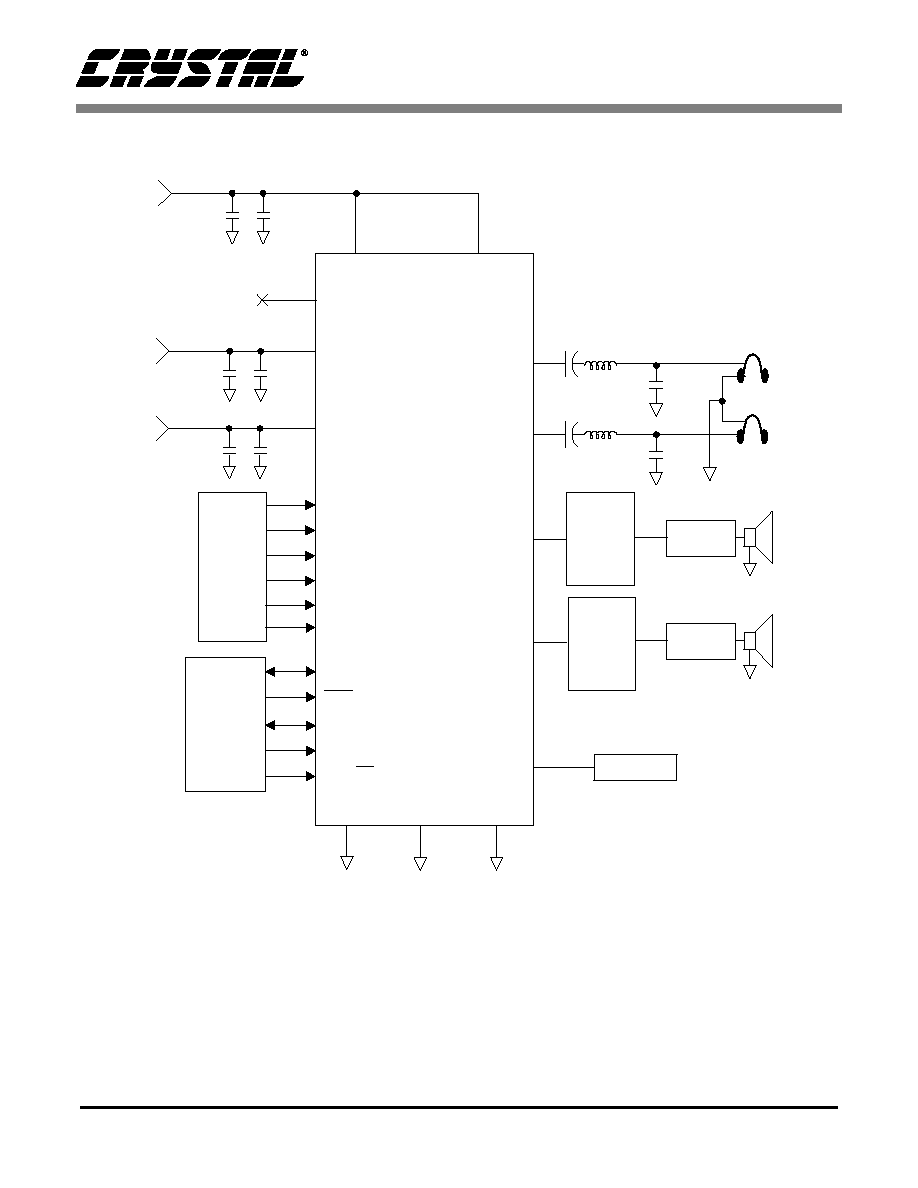
CS44210
12
DS539PP1
MCLK
LRCK
SC LK
SDIN1
RST
VA_HPB
CS44210
2.4 to 5.0 V
Supply
100 µF
+
VA_HPA
Supply
1.0 µF
+
VL
19
20
8
7
2
5
3
18
21
16
1
9
4
15
14
2.4 to 5.0 V
Supply
1.0 µF
+
VD
6
2.4 to 5.0 V
24
SDIN2 *
SDIN3 *
AD1/CDOUT
2 3
10
DRIVER_A
17
22
0.15
µF
0.15
µF
16
Headphones
GND
GND
GND
0.1 µF
AD0/CS
SCL/CCLK
SDA/CDIN
0.1 µF
0.1 µ F
HP_A
HP_B
TSTIN
12
11
SYNC_CLK
Sync Clock
13
DRIVER_B
Output
Filter
Output
Filter
220 µ F
100 µH
220 µF
100 µH
Cout
+
+
Cout
MOSFET
Driver
&
Power
Stage
MOSFET
Driver
&
Power
Stage
* Unused SDIN pins should be connected to GND
Digital
Audio
Source
µC/
Mode
Control
Figure 5. Typical CS44210 Connection Diagram Control Port Mode
CS44210
DS539PP1
13
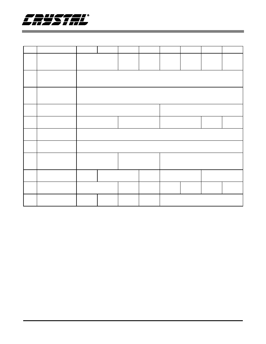
3. REGISTER QUICK REFERENCE
Addr
Function
7
6
5
4
3
2
1
0
2h
Power and Muting
Control
SZC1
SZC0
PDN
FLT
RUPBYP
RDNBYP
Reserved
Reserved
default
1
0
1
0
0
0
0
0
3h
Channel A
Volume Control
VOLA7
VOLA6
VOLA5
VOLA4
VOLA3
VOLA2
VOLA1
VOLA0
default
0
0
0
0
0
0
0
0
4h
Channel B
Volume Control
VOLB7
VOLB6
VOLB5
VOLB4
VOLB3
VOLB2
VOLB1
VOLB0
default
0
0
0
0
0
0
0
0
5h
Tone Control
BB3
BB2
BB1
BB0
TB3
TB2
TB1
TB0
default
0
0
0
0
0
0
0
0
6h
Mode Control 1
BBCF1
BBCF0
TBCF1
TBCF0
TC1
TC0
TC_EN
LIM_EN
default
0
0
0
0
0
0
0
0
7h
Limiter Attack Rate
ARATE7
ARATE6
ARATE5
ARATE4
ARATE3
ARATE2
ARATE1
ARATE0
default
0
0
0
1
0
0
0
0
8h
Limiter Release Rate
RRATE7
RRATE6
RRATE5
RRATE4
RRATE3
RRATE2
RRATE1
RRATE0
default
0
0
1
0
0
0
0
0
9h
Volume and Mixing
Control
IS1
IS0
RMP_SP1 RMP_SP0
ATAPI3
ATAPI2
ATAPI1
ATAPI0
default
0
0
0
1
1
0
0
1
Ah
Mode Control2
MCLKDIV
CLKDV1
CLKDV0
DBS
FRQSFT1 FRQSFT0
DEM1
DEM0
default
0
0
0
0
0
0
0
0
Bh
Mode Control 3
DIF1
DIF0
A=B
VCBYP
CP_EN
FREEZE
Reserved
Reserved
default
0
0
0
0
0
0
0
0
Ch
Revision Indicator
Reserved
Reserved
Reserved
Reserved
REV3
REV2
REV1
REV0
default
0
0
0
0
Read Only Read Only Read Only Read Only
Table 1. Register Quick Reference

CS44210
14
DS539PP1
4. REGISTER DESCRIPTIONS
4.1 Power and Muting Control (address 02h)
4.1.1 SOFT RAMP AND ZERO CROSS CONTROL (SZC)
Default = 10
00 - Immediate Change
01 - Zero Cross Control
10 - Ramped Control
11 - Reserved
Function:
Immediate Change
When Immediate Change is selected, all level changes will take effect immediately in one step.
Zero Cross Control
Zero Cross Enable dictates that signal level changes, either by attenuation changes or muting, will occur
on a signal zero crossing to minimize audible artifacts. The requested level change will occur after a
time-out period of 512 sample periods (10.7 ms at 48 kHz sample rate) if the signal does not encounter a
zero crossing. The zero cross function is independently monitored and implemented for each channel.
Ramped Control
Soft Ramp allows level changes, both muting and attenuation, to be implemented by incrementally ramp-
ing, in 1/8 dB steps, from the current level to the new level at a rate of 1 dB per 8 left/right clock periods.
Note: Ramped Control is not available in Double Speed Mode.
4.1.2 POWER DOWN (PDN)
Default = 1
0 - Disabled
1 - Enabled
Function:
The entire device will enter a low-power state when this function is enabled, and the contents of the control
registers are retained in this mode. The power-down bit defaults to `enabled' on power-up and must be
disabled before normal operation in Control Port mode can occur.
7
6
5
4
3
2
1
0
SZC1
SZC0
PDN
FLT
RUPBYP
RDNBYP
Reserved
Reserved
1
0
1
0
0
0
0
0

CS44210
DS539PP1
15
4.1.3 FLOAT OUTPUT (FLT)
Default = 0
0 - Disabled
1 - Enabled
Function:
When enabled, this bit will cause the headphone output of the CS44210 to float when in the power down
state (PDN=1). The float function can be used in single-ended applications to maintain the charge on the
DC-blocking capacitor during power transients. On power transitions, the output will quickly change to the
bias point, however, if the DC-blocking capacitor still has a full charge, as in short power cycles, the tran-
sition will be very small, often inaudible. Refer to Section 6.4
.
4.1.4 RAMP UP BYPASS (RUPBYP)
Default = 0
0 - Normal
1 - Bypass
Function:
When in normal mode, the duty cycle of the output PWM signal is increased at a rate determined by the
Ramp Speed variable (RMP_SPx). Normal mode is used in Single Ended applications to reduce pops in
the output caused by the DC-blocking capacitor. When the ramp up function is bypassed in Single Ended
applications, there will be an abrupt change in the output signal. Refer to Section 6.4.
4.1.5 RAMP DOWN BYPASS (RDNBYP)
Default = 0
0 - Disabled
1 - Enabled
Function:
When in normal mode, the duty cycle of the output PWM signal is decreased at a rate determined by the
Ramp Speed variable (RMP_SPx). Normal mode is used in Single Ended applications to reduce pops in
the output caused by the DC-blocking capacitor and changes in bias conditions. When the ramp down
function is bypassed in Single Ended applications, there will be an abrupt change in the output signal. Re-
fer to Section 6.4.
4.2 Channel A Volume Control (address 03h) (VOLA)
4.3 Channel B Volume Control (address 04h) (VOLB)
Default = 0 dB (No attenuation)
Function:
The Volume Control registers allow independent control of the signal levels in 1 dB increments from +18
to -96 dB. Volume settings are decoded using a 2's complement code, as shown in Table 2. The volume
changes are implemented as dictated by the Soft and Zero Cross bits. All volume settings less than -96 dB
are equivalent to muting the channel via the ATAPI bits (see Section 4.8.3).
7
6
5
4
3
2
1
0
VOLx7
VOLx6
VOLx5
VOLx4
VOLx3
VOLx2
VOLx1
VOLx0
0
0
0
0
0
0
0
0

CS44210
16
DS539PP1
Note: All volume settings greater than +18 dB are interpreted as +18 dB.
4.4 Tone Control (address 05h)
4.4.1 BASS BOOST LEVEL (BB)
Default = 0 dB (No Bass Boost)
Function:
The level of the shelving bass boost filter is set by Bass Boost Level. The level can be adjusted in 1 dB
increments from 0 to +12 dB of boost. Boost levels are decoded as shown in Table 3. Levels above
+12 dB are interpreted as +12 dB.
4.4.2 TREBLE BOOST LEVEL (TB)
Default = 0 dB (No Treble Boost)
Function:
The level of the shelving treble boost filter is set by Treble Boost Level. The level can be adjusted in 1 dB
increments from 0 to +12 dB of boost. Boost levels are decoded as shown in Table 4. Levels above
+12 dB are interpreted as +12 dB.
Note: Treble Boost is not available in Double Speed Mode.
Binary Code
Decimal Value
Volume Setting
00001010
12
+12 dB
00000111
7
+7 dB
00000000
0
0 dB
11000100
-60
-60 dB
10100110
-90
-90 dB
Table 2. Example Volume Settings
7
6
5
4
3
2
1
0
BB3
BB2
BB1
BB0
TB3
TB2
TB1
TB0
0
0
0
0
0
0
0
0
Binary Code
Decimal Value
Boost Setting
0000
0
0 dB
0010
2
+2 dB
1010
6
+6 dB
1001
9
+9 dB
1100
12
+12 dB
Table 3. Example Bass Boost Settings
Binary Code
Decimal Value
Boost Setting
0000
0
0 dB
0010
2
+2 dB
1010
6
+6 dB
1001
9
+9 dB
1100
12
+12 dB
Table 4. Example Treble Boost Settings

CS44210
DS539PP1
17
4.5 Mode Control 1 (address 06h)
4.5.1 BASS BOOST CORNER FREQUENCY (BBCF)
Default = 00
00 - 50 Hz
01 - 100 Hz
10 - 200 Hz
11 - Reserved
Function:
The bass boost corner frequency is user-selectable. The corner frequency is a function of LRCK (sam-
pling frequency), the DBS bit and the BBCF bits as shown in Table 5 and Table 6.
4.5.2 TREBLE BOOST CORNER FREQUENCY (TBCF)
Default = 00
00 - 2 kHz
01 - 4 kHz
10 - 7 kHz
11 - Reserved
Function:
The treble boost corner frequency is user selectable. The corner frequency is a function of LRCK (sam-
pling frequency) and the TBCF bits as shown in Table 7.
Note: Treble Boost is not available in Double Speed Mode.
7
6
5
4
3
2
1
0
BBCF1
BBCF0
TBCF1
TBCF0
TC1
TC0
TC_EN
LIM_EN
0
0
0
0
0
0
0
0
BBCF
Fs
LRCK in Single Speed Mode (DBS=0)
48 kHz
24 kHz
12 kHz
8 kHz
00
50 Hz
25 Hz
12.5 Hz
8.33 Hz
01
100 Hz
50 Hz
25 Hz
16.7 Hz
10
200 Hz
100 Hz
50 Hz
33.3 Hz
11
Reserved
Reserved
Reserved
Reserved
Table 5. Base Boost Corner Frequencies in Single Speed Mode
BBCF
Fs
LRCK in Double Speed Mode (DBS=1)
96 kHz
48 kHz
24 kHz
16 kHz
00
50 Hz
25 Hz
12.5 Hz
8.33 Hz
01
100 Hz
50 Hz
25 Hz
16.7 Hz
10
200 Hz
100 Hz
50 Hz
33.3 Hz
11
Reserved
Reserved
Reserved
Reserved
Table 6. Base Boost Corner Frequencies in Double Speed Mode

CS44210
18
DS539PP1
4.5.3 TONE CONTROL MODE (TC)
Default = 00
00 - All settings are taken from user registers
01 - 12 dB of Bass Boost at 100 Hz and 6 dB of Treble Boost at 7 kHz (at LRCK = 48 kHz)
10 - 8 dB of Bass Boost at 100 Hz and 4 dB of Treble Boost at 7 kHz (at LRCK = 48 kHz)
11 - 4 dB of Bass Boost at 100 Hz and 2 dB of Treble Boost at 7 kHz (at LRCK = 48 kHz)
Function:
The Tone Control Mode bits determine how the Bass Boost and Treble Boost features are configured.
The user-defined settings from the Bass and Treble Boost Level and Corner Frequency registers are used
when these bits are set to `00'. Alternately, one of three pre-defined settings may be used (these settings
are a function of LRCK - refer to tables 5, 6, and 7).
Note:
Treble boost is not available in Double Speed Mode.
4.5.4 TONE CONTROL ENABLE (TC_EN)
Default = 0
0 - Disabled
1 - Enabled
Function:
The Bass Boost and Treble Boost features are active when this function is enabled.
4.5.5 PEAK SIGNAL LIMITER ENABLE (LIM_EN)
Default = 0
0 - Disabled
1 - Enabled
Function:
The CS44210 will limit the maximum signal amplitude to prevent clipping when this function is enabled.
Peak Signal Limiting is performed by first decreasing the Bass and Treble Boost Levels. If the signal is
still clipping, the digital attenuation is increased. The attack rate is determined by the Limiter Attack Rate
register.
Once the signal has dropped below the clipping level, the attenuation is decreased back to the user se-
lected level followed by the Bass Boost being increased back to the user selected level. The release rate
is determined by the Limiter Release Rate register.
Note: The A=B bit should be set to `1' for optimal limiter performance.
TBCF
Fs
LRCK in Single Speed Mode (DBS=0)
48 kHz
24 kHz
12 kHz
8 kHz
00
2 kHz
1 kHz
0.5 kHz
0.33 kHz
01
4 kHz
2 kHz
1 kHz
0.67 kHz
10
7 kHz
3.5 kHz
1.75 kHz
1.17 kHz
11
Reserved
Reserved
Reserved
Reserved
Table 7. Treble Boost Corner Frequencies in Single Speed Mode
CS44210
DS539PP1
19
4.6 Limiter Attack Rate (address 07h) (ARATE)
Default = 10h - 2 LRCK's per 1/8 dB
Function:
The limiter attack rate is user-selectable. The rate is a function of sampling frequency, As, and the value
in the Limiter Attack Rate register. Rates are calculated using the function RATE = 32/{value}, where {val-
ue} is the decimal value in the Limiter Attack Rate register and RATE is in LRCK's per 1/8 dB of change.
Note: A value of zero in this register is not recommended, as it will induce erratic behavior of the limiter.
Use the LIM_EN bit to disable the limiter function (see "Peak Signal Limiter Enable (LIM_EN)").
4.7 Limiter Release Rate (address 08h) (RRATE)
Default = 20h - 16 LRCK's per 1/8 dB
Function:
The limiter release rate is user-selectable. The rate is a function of sampling frequency, Fs, and the value
in the Limiter Release Rate register. Rates are calculated using the function RATE = 512/{value}, where
{value} is the decimal value in the Limiter Release Rate register and RATE is in LRCK's per 1/8 dB of
change.
Note: A value of zero in this register is not recommended, as it will induce erratic behavior of the limiter.
Use the LIM_EN bit to disable the limiter function (see "Peak Signal Limiter Enable (LIM_EN)").
7
6
5
4
3
2
1
0
ARATE7
ARATE6
ARATE5
ARATE4
ARATE3
ARATE2
ARATE1
ARATE0
0
0
0
1
0
0
0
0
Binary Code
Decimal Value
LRCK's per 1/8 dB
00000001
1
32
00010100
20
1.6
00101000
40
0.8
00111100
60
0.53
01011010
90
0.356
Table 8. Example Limiter Attack Rate Settings
7
6
5
4
3
2
1
0
RRATE7
RRATE6
RRATE5
RRATE4
RRATE3
RRATE2
RRATE1
RRATE0
0
0
1
0
0
0
0
0
Binary Code
Decimal Value
LRCK's per 1/8 dB
00000001
1
512
00010100
20
25
00101000
40
12
00111100
60
8
01011010
90
5
Table 9. Example Limiter Release Rate Settings

CS44210
20
DS539PP1
4.8 Volume and Mixing Control (address 09h)
4.8.1 INPUT MUX SELECTION (IS)
Default = 00
00 - Selects SDIN1 as input
01 - Selects SDIN2 as input
10 - Selects SDIN3 as input
11 - Reserved
Function:
The Input Mux Selector determines which SDIN input is selected.
4.8.2 RAMP SPEED (RMP_SP)
Default = 01
00 - Ramp speed = approximately 0.1 seconds
01 - Ramp speed = approximately 0.2 seconds
10 - Ramp speed = approximately 0.3 seconds
11 - Ramp speed = approximately 0.65 seconds
Function:
This feature is used in Single Ended applications to reduce pops in the output caused by the DC-blocking
capacitor. When in control port mode, the Ramp Speed sets the time for the PWM signal to linearly ramp
up and down from the bias point (50% PWM duty cycle). Refer to Section 6.4.
4.8.3 ATAPI CHANNEL MIXING AND MUTING (ATAPI)
Default = 1001 - HP_A = L, HP_B = R (Stereo)
Function:
The CS44210 implements the channel mixing functions of the ATAPI CD-ROM specification. Refer to
Table 10 and Figure 6 for additional information.
Note: All mixing functions occur prior to the digital volume control.
7
6
5
4
3
2
1
0
IS1
IS0
RMP_SP1
RMP_SP0
ATAPI3
ATAPI2
ATAPI1
ATAPI0
0
0
0
0
1
0
0
1
CS44210
DS539PP1
21
ATAPI3
ATAPI2
ATAPI1
ATAPI0
HP_A
HP_B
0
0
0
0
MUTE
MUTE
0
0
0
1
MUTE
R
0
0
1
0
MUTE
L
0
0
1
1
MUTE
[(L+R)/2]
0
1
0
0
R
MUTE
0
1
0
1
R
R
0
1
1
0
R
L
0
1
1
1
R
[(L+R)/2]
1
0
0
0
L
MUTE
1
0
0
1
L
R
1
0
1
0
L
L
1
0
1
1
L
[(L+R)/2]
1
1
0
0
[(L+R)/2]
MUTE
1
1
0
1
[(L+R)/2]
R
1
1
1
0
[(L+R)/2]
L
1
1
1
1
[(L+R)/2]
[(L+R)/2]
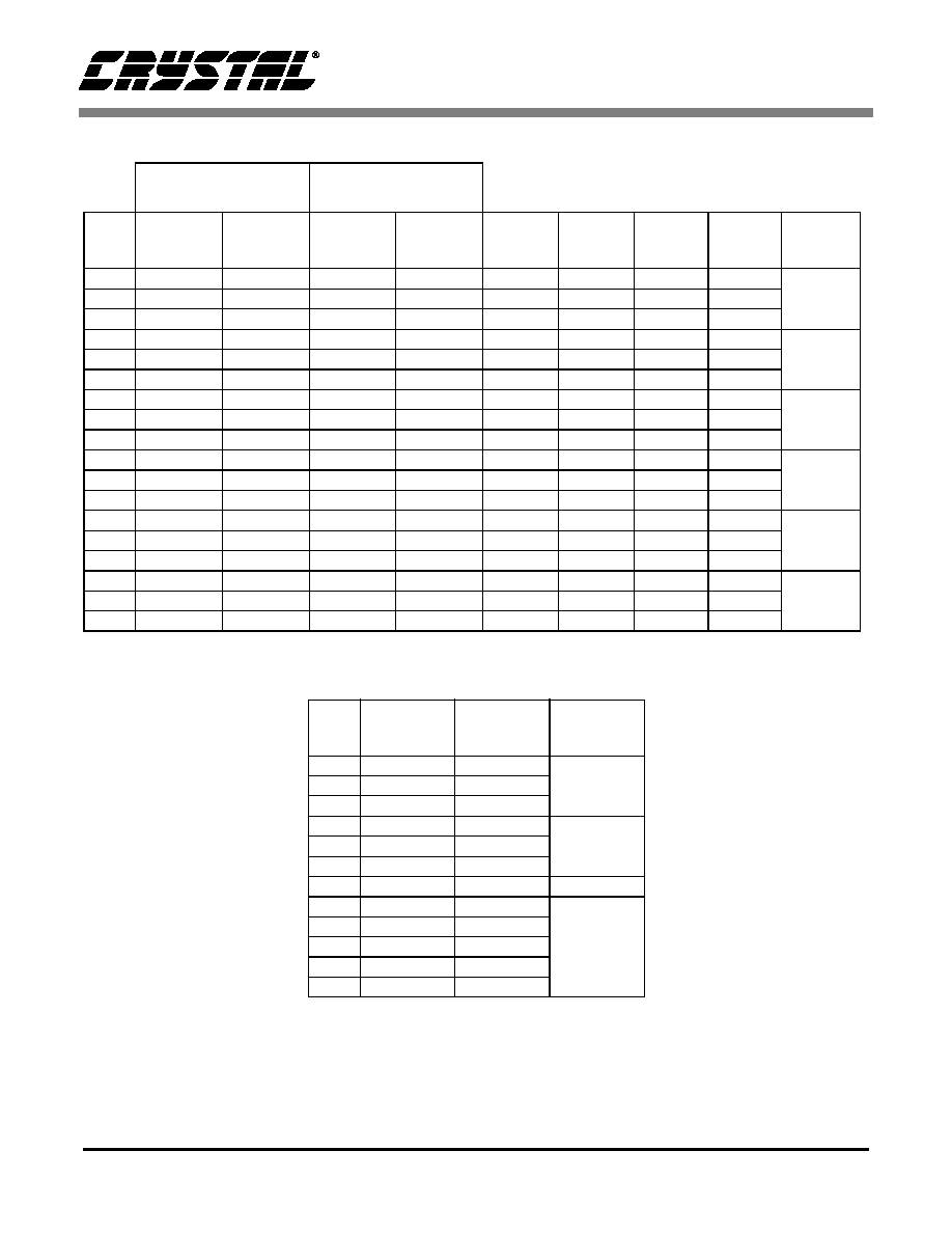
Table 10. ATAPI Decode
HP_A
HP_B
Left Channel
Audio Data
Right Channel
Audio Data
Channel B
Digital
Volume
Control
EQ
Channel A
Digital
Volume
Control
EQ
& Mute
& Mute
Figure 6. Dynamics Control Block Diagram

CS44210
22
DS539PP1
4.9 Mode Control 2 (address 0Ah)
4.9.1 MASTER CLOCK DIVIDE ENABLE (MCLKDIV)
Default = 0
Function:
The MCLKDIV bit enables a circuit which divides the externally applied MCLK signal by 2 prior to all other
internal circuitry. MCLKDIV, DBS, CLKDIV and FRQSFT are set per the user's MCLK and LRCK require-
ments. Refer to Tables 11, 12, 13, 14, and
Section 6.2.
4.9.2 CLOCK DIVIDE (CLKDIV)
Default = 00
Function:
MCLKDIV, DBS, CLKDIV and FRQSFT are set per the user's MCLK and LRCK requirements. Refer to
Tables 11, 12, 13, 14, and
Section 6.2
.
4.9.3 DOUBLE SPEED MODE (DBS)
Default = 0
0 - Single Speed
1 - Double Speed (DBS)
Function:
Single Speed supports 8kHz to 50 kHz sample rates and Double Speed supports 50 kHz to 96kHz sample
rates. MCLKDIV, DBS, CLKDIV and FRQSFT are set per the user's MCLK and LRCK requirements. Refer
to Tables 11, 12, 13, 14, and
Section 6.2.
Note: De-emphasis, ramp control, and treble control are not available in Double Speed Mode.
4.9.4 FREQUENCY SHIFT (FRQSFT)
Default = 00
Function:
MCLKDIV, DBS, CLKDIV and FRQSFT are set per the user's MCLK and LRCK requirements. Refer to
Tables 11, 12, 13, 14, and Section 6.2.
7
6
5
4
3
2
1
0
MCLKDIV
CLKDV1
CLKDV0
DBS
FRQSFT1
FRQSFT0
DEM1
DEM0
0
0
0
0
0
0
0
0
CS44210
DS539PP1
23
DBS = 0
MCLKDIV = 0
DBS = 0
MCLKDIV = 1
LRCK
(kHz)
MCLK/
LRCK
MCLK
(MHz)
MCLK/
LRCK
MCLK
(MHz)
FRQSFT1 FRQSFT0
CLKDIV1
CLKDIV0
PWM
Switching
Freq. (kHz)
48
256
12.288
512
24.576
0
0
0
0
48
384
18.432
768
36.864
0
0
0
1
384
48
512
24.576
1024
49.152
0
0
1
0
44.1
256
11.2896
512
22.5792
0
0
0
0
44.1
384
16.9344
768
33.8688
0
0
0
1
352.8
44.1
512
22.5792
1024
45.1584
0
0
1
0
32
512
16.384
1024
32.768
0
1
0
0
32
768
24.576
1536
49.152
0
1
0
1
512
32
1024
32.768
2048
65.536
0
1
1
0
24
512
12.288
1024
24.576
0
1
0
0
24
768
18.432
1536
36.864
0
1
0
1
384
24
1024
24.576
2048
49.152
0
1
1
0
12
1024
12.288
2048
24.576
1
0
0
0
12
1536
18.432
3072
36.864
1
0
0
1
384
12
2048
24.576
4096
49.152
1
0
1
0
8
1536
12.288
3072
24.576
1
1
0
0
8
2304
18.432
4608
36.864
1
1
0
1
384
8
3072
24.576
6144
49.152
1
1
1
0
Table 11. Single Speed Clock Modes - Control Port Mode
LRCK
(kHz)
MCLK/
LRCK
MCLK
(MHz)
PWM
Switching
Freq. (kHz)
48
256
12.288
48
384
18.432
384
48
512
24.576
44.1
256
11.2896
44.1
384
16.9344
352.8
44.1
512
22.5792
32
1024
32.768
512
24
1024
24.576
12
2048
24.576
8
1536
12.288
384
8
2304
18.432
8
3072
24.576
Table 12. Single Speed Clock Modes - Stand-Alone Mode
CS44210
24
DS539PP1
4.9.5 DE-EMPHASIS CONTROL (DEM)
Default = 00
00 - Disabled
01 - 44.1 kHz
10 - 48 kHz
11 - 32 kHz
Function:
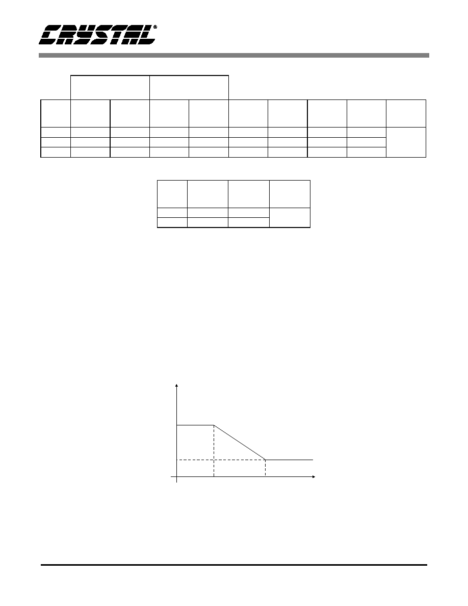
Selects the appropriate digital filter to maintain the standard 15
µs/50 µs digital de-emphasis filter re-
sponse at 32, 44.1 or 48 kHz sample rates (see Figure 7).
Note: De-emphasis is not available in double speed mode.
DBS = 1
MCLKDIV = 0
DBS = 1
MCLKDIV = 1
LRCK
(kHz)
MCLK/
LRCK
MCLK
(MHz)
MCLK/
LRCK
MCLK
(MHz)
FRQSFT1
FRQSFT0
CLKDIV1
CLKDIV0
PWM
Switching
Freq. (kHz)
96
128
12.288
256
24.576
0
0
0
0
96
192
18.432
384
36.864
0
0
0
1
384
96
256
24.576
512
49.152
0
0
1
0
Table 13. Double Speed Clock Modes - Control Port Mode
LRCK
(kHz)
MCLK/
LRCK
MCLK
(MHz)
PWM
Switching
Freq. (kHz)
96
128
12.288
384
96
192
18.432
Table 14. Double Speed Clock Modes - Stand-Alone Mode
Gain
dB
-10dB
0dB
Frequency
T2 = 15 µs
T1=50 µs
F1
F2
3.183 kHz
10.61 kHz
Figure 7. De-Emphasis Curve

CS44210
DS539PP1
25
4.10 Mode Control 3 (address 0Bh)
4.10.1 DIGITAL INTERFACE FORMATS (DIF)
Default = 00
00 - I
2
S
01 - Right Justified, 16 bit
10 - Left Justified
11 - Right Justified, 24 bit
Function:
The required relationship between the Left/Right clock, serial clock and serial data is defined by the Digital
Interface Format and the options are detailed in figures 19 through 22.
4.10.2 CHANNEL A VOLUME = CHANNEL B VOLUME (A=B)
Default = 0
0 - Disabled
1 - Enabled
Function:
The HP_A and HP_B volume levels and the DRIVER_x outputs are independently controlled by the A and
the B Channel Volume Control Bytes when this function is disabled. The volume on both HP_A, HP_B,
DRIVER_A and DRIVER_B are determined by the A Channel Volume Control Byte and the B Channel
Byte is ignored when this function is enabled.
4.10.3 VOLUME CONTROL BYPASS (VCBYP)
Default = 0
0 - Disabled
1 - Enabled
Function:
The digital volume control section is bypassed when this function is enabled. This disables the digital vol-
ume control, muting, bass boost, treble boost, limiting, and ATAPI functions.
4.10.4 CONTROL PORT ENABLE (CP_EN)
Default = 0
0 - Disabled
1 - Enabled
Function:
This bit defaults to 0, allowing the device to power-up in Stand-Alone mode. The Control port mode can
be accessed by setting this bit to 1. This will allow the operation of the device to be controlled by the reg-
isters and the pin definitions will conform to Control Port Mode. Refer to Section 7.1
.
7
6
5
4
3
2
1
0
DIF1
DIF0
A=B
VCBYP
CP_EN
FREEZE
HPSEN
Reserved
0
0
0
0
0
0
0
0
CS44210
26
DS539PP1
4.10.5 FREEZE (FREEZE)
Default = 0
0 - Disabled
1 - Enabled
Function:
This function allows modifications to be made to the registers without the changes being taking effect until
the FREEZE is disabled. To make multiple changes in the Control port registers take effect simultaneous-
ly, you will first enable the FREEZE Bit, then make all register changes, then Disable the FREEZE bit.
4.11 Revision Indicator (address 0Ch)[Read Only]
Default = none
0000 - Revision A
0001 - Revision B
0010 - Revision C
etc.
Function:
This read-only register indicates the revision level of the device.
7
6
5
4
3
2
1
0
Reserved
Reserved
Reserved
Reserved
REV3
REV2
REV1
REV0
0
0
0
0
0
0
0
0

CS44210
DS539PP1
27
5. PIN DESCRIPTION
1
2
3
4
5
6
7
8
9
10
11
12
13
14
24
23
22
21
20
19
18
17
16
15
Serial Data 2
SDIN2
SDIN3
Serial Data 3
Serial Data 1
SDIN1
RST
Reset
Left/Right Clock
LRCK
GND
Headphone B Ground
Serial Clock
SCLK
HP_B
Headphone B Output
Master Clock
MCLK
VA_HPB
Headphone B Power
Digital Power
VD
VA_HPA
Headphone A Power
Ground
GND
HP_A
Headphone A Output
Interface Power
VL
GND
Headphone A Ground
SCL/CCLK/DIF0 SCL/CCLK/DIF0
SDA/CDIN/DEM SDA/CDIN/DEM
Addr0/ChipSel/DIF1
AD0/CS/DIF1
AD1/CDOUT
Addr1/CDOUT
Sync Clock
SYNC_CLK
DRIVER_A
Driver Output A
Test In
TSTIN
DRIVER_B
DriverOutput B
SDIN1
SDIN2
SDIN3
2
1
24
Serial Audio Data Input (Input) - Input for two's complement serial audio data. Unused inputs
should be grounded.
LRCK
3
Left Right Clock (Input) - Determines which channel, Left or Right, is currently active on the
serial audio data line. The frequency of the left/right clock must be at the audio sample rate, Fs.
SCLK
4
Serial Clock (Input) - Serial clock for the serial audio interface.
MCLK
5
Master Clock (Input) - Clock source for the PWM modulator and digital filters. Table 11, 12, 13
and 14 illustrate several standard audio sample rates and the required master clock frequen-
cies.
VD
6
Digital Power (Input) - Positive power supply for the digital section. Refer to "Recommended
Operating Conditions" for appropriate voltages.
GND
7, 17
& 22
Ground (Input) - Ground Reference.
VL
8
Logic Power (Input) - Determines the required signal level for the digital input/output. Refer to
"Recommended Operating Conditions" for appropriate voltages.
Sync Clock
11
SYNC_CLK (Output) - Provides a high frequency clock signal at 32 x PWM switching frequency
to synchronize external circuitry, if needed.
TSTIN
12
Test In (Input) - This pin is not used and must remaing floating.
DRIVER_A
DRIVER_B
14
13
DRIVER OUTPUTS(Outputs) Outputs used to drive external power devices.
HP_A
HP_B
18
21
Headphone Outputs (Output) - PWM Headphone Outputs. An external LC filter should be
added to suppress high frequency switching noise. A DC blocking capacitor is also required.
Refer to Typical Connection Diagrams.
VA_HPA
VA_HPB
19
20
Headphone Amplifier Power (Input) - Positive power supply for the headphone amplifier.
Refer to "Recommended Operating Conditions" for appropriate voltages.
RST
23
Reset (Input) - The device enters a low power mode and all internal registers are reset to their
default settings when low. The control port cannot be accessed when Reset is low. See Sec-
tion 6.5
Control Port
Definitions
SCL/CCLK
9
Serial Control Port Clock (Input) - Serial clock for the serial control port. Requires an external
pull-up resistor to VL in Two-Wire mode.

CS44210
28
DS539PP1
ADO/CS
10
Address Bit 0 (Two-Wire) / Control Port Chip Select (SPI) (Input) - AD0 is a chip address pin
Two-Wire mode; CS is used to enable the control port interface.
AD1/CDOUT
15
AD1/CDOUT - Address Bit 1 (Two Wire) / Serial Control data out (SPI) (Input/Output) - In
Two- Wire mode, AD1 is a chip address pin. In SPI mode, CDOUT is the output data from the
control port interface.
SDA/CDIN
16
Serial Control Data (Input/Output) - SDA is a data I/O line in Two-Wire mode and requires an
external pull-up resistor to the logic interface voltage. CDIN is the input data line for the control
port interface in SPI mode.
Stand Alone
Definitions
DIF0
DIF1
9
10
Digital Interface Format (Input) - The required relationship between the Left/Right clock, serial
clock and serial data is defined by the Digital Interface Format and the options are detailed
below
AD1/CDOUT
15
Non-applicable (input) - non-functional in this mode should be connected to ground.
DEM
16
De-emphasis Control (Input) - Selects the standard 15
µs/50 µs digital de-emphasis filter
response at 44.1 kHz sample rates. NOTE: De-emphasis is not available in Double or Quad
Speed Modes. When DEM is grounded, de-emphasis is disabled.
.
DIF1
DIF0
DESCRIPTION
FIGURE
0
0
Left Justified, up to 24-bit data
19
0
1
Right Justified, 24 -bit Data
20
1
0
I
2
S, up to 24-bit data
21
1
1
Right Justified, 16-bit Data
22
Table 15. Digital Interface Format - DIF1 and DIF0
(St
d Al
M d )

CS44210
DS539PP1
29
6.
APPLICATIONS
6.1 Grounding and Power Supply Decoupling
As with any switching converter, the CS44210 re-
quires careful attention to power supply and
grounding arrangements to optimize performance.
Figures 4 and 5 show the recommended power ar-
rangement with VD, VA_HPx, and VL connected
to clean supplies. Decoupling capacitors should be
located as close to the device package as possible.
If desired, all supply pins may be connected to the
same supply, but a decoupling capacitor should still
be used on each supply pin.
6.2 Clock Modes
One of the characteristics of a PWM amplifier is
that the frequency content of out-of-band noise
generated by the modulator is dependent on the
PWM switching frequency. The systems designer
will specify the external filter based on this switch-
ing frequency. The obvious implementation in a
digital PWM system is to directly lock the PWM
switching rate to the incoming data sample rate.
However, this would require a tuneable filter to at-
tentuate the switching frequency across the range
of possible sample rates. To simplify the external
filter design and to accommodate sample rates
ranging from 8 kHz to 96 kHz the CS44210 Con-
troller uses several clock modes that keep the PWM
switching frequency in a small range.
In control port mode, for operation at a particular
sample rate the user selects register settings (refer
to Section 4.9 and Tables 11 and 13) based on their
MCLK and MCLK/LRCK parameters. When us-
ing Stand-Alone mode, refer to Tables 12 and 14
for available clock modes.
6.3 De-Emphasis
The CS44210 includes on-chip digital de-empha-
sis. Figure 7 shows the de-emphasis curve. The fre-
quency response of the de-emphasis curve will
scale proportionally with changes in sample rate,
Fs.
The de-emphasis feature is included to accommo-
date older audio recordings that utilize pre-empha-
sis equalization as a means of noise reduction.
6.4 PWM PopGuard Transient Control
The CS44210 uses PopGuard
Æ
technology to mini-
mize the effects of output transients during pow-
er-up and power-down. This technique minimizes
the audio transients commonly produced by sin-
gle-ended, single-supply converters when it is im-
plemented with external DC-blocking capacitors
connected in series with the audio outputs.
When the device is initially powered-up, the
DRIVER_x, and HP_x outputs are clamped to
GND. Following a delay each output begins to in-
crease the PWM duty cycle toward the quiescent
voltage point. By a speed set by the RMP_SP bit,
the DRIVER_x and HP_x outputs will later reach
the bias point (50% PWM duty cycle), and audio
output begins. This gradual voltage ramping allows
time for the external DC-blocking capacitor to
charge to the quiescent voltage, minimizing the
power-up transient.
To prevent transients at power-down, the device
must first enter its power-down state. When this oc-
curs, audio output ceases and the PWM duty cycle
is decreased until the DRIVER_x and HP_x out-
puts reach GND. The time required to reach GND
is determined by the RMP_SP bits. This allows the
DC-blocking capacitors to slowly discharge. Once
this charge is dissipated, the power to the device
may be turned off, and the system is ready for the
next power-on.
To prevent an audio transient at the next power-on,
the DC-blocking capacitors must fully discharge
before turning off the power or exiting the pow-
er-down state. If full discharge does not occur, a
transient will occur when the audio outputs are ini-
tially clamped to GND. The time that the device
must remain in the power-down state is related to
the value of the DC-blocking capacitance and the
output load. For example, with a 220 µF capacitor

CS44210
30
DS539PP1
and a 16 ohm load on the headphone outputs, the
minimum power-down time will be approximately
0.4 seconds.
Note that ramp up and ramp down period can be set
to zero with the RUPBYP and RDNBYP bits re-
spectively.
6.5 Recommended Power-up Sequence
6.5.1 Stand Alone Mode
1. Hold RST low until the power supply, master,
and left/right clocks are stable. In this state, the
control port is reset to its default settings and the
HP_x and DRIVER_x lines will remain low.
2. Bring RST high. The device will remain in a low
power state and will initiate the Stand-Alone pow-
er-up sequence. The control port will be accessible
at this time.
6.5.2 Control Port Mode
1. Hold RST low until the power supply, master,
and left/right clocks are stable. In this state, the
control port is reset to its default settings and the
HP_x and DRIVER_x lines will remain low.
2. Bring RST high. The device will remain in a low
power state and will initiate the Stand-Alone pow-
er-up sequence. The control port will be accessible
at this time.
3. On the CS44210 the control port pins are shared
with stand-alone configuration pins. To enable the
control port, the user must set the CP_EN bit. This
is done by performing a Two-Wire or SPI write.
Once the control port is enabled, these pins are ded-
icated to control port functionality.
To prevent audible artifacts the CP_EN bit (see
Section 4.10.4) should be set prior to the comple-
tion of the Stand-Alone power-up sequence, ap-
proximately 21mS. Writing this bit will halt the
Stand-Alone power-up sequence and initialize the
control port to its default settings. Note, the CP_EN
bit can be set any time after RST goes high; how-
ever, setting this bit after the Stand-Alone pow-
er-up sequence has completed can cause audible
artifacts.

CS44210
DS539PP1
31
7. CONTROL PORT INTERFACE
The control port is used to load all the internal set-
tings. The operation of the control port may be
completely asynchronous with the audio sample
rate. However, to avoid potential interference prob-
lems, the control port pins should remain static if
no operation is required.
The CS44210 has MAP auto increment capability,
enabled by the INCR bit in the MAP register,
which is the MSB. If INCR is 0, then the MAP will
stay constant for successive writes. If INCR is set
to 1, then MAP will auto increment after each byte
is written, allowing block reads or writes of succes-
sive registers.
7.1 Format Selection
The control port has 2 formats: SPI and Two-Wire,
with the CS44210 operating as a slave device.
If Two-Wire operation is desired, AD0/CS should
be tied to VL or GND. If the CS44210 ever detects
a high to low transition on AD0/CS after power-up
and after the control port is activated, SPI format
will be selected.
7.2 Two-Wire Format
In Two-Wire Format, SDA is a bidirectional data
line. Data is clocked into and out of the part by the
clock, SCL, with a clock to data relationship as
shown in Figure 8. The receiving device should
send an acknowledge (ACK) after each byte re-
ceived. There is no CS pin. Pins AD0 and AD1
forms the partial chip address and should be tied to
VL or GND as required. The upper 6 bits of the 7-
bit address field must be 001000.
Note: MCLK is required during all two-wire
transactions. The Two-Wire format is compatible
with the I
2
C protocol.
7.2.1 Writing in Two-Wire Format
To communicate with the CS44210, initiate a
START condition of the bus. Next, send the chip
address. The eighth bit of the address byte is the
R/W bit (low for a write). The next byte is the
Memory Address Pointer, MAP, which selects the
register to be read or written. The MAP is then fol-
lowed by the data to be written. To write multiple
registers, continue providing a clock and data,
waiting for the CS44210 to acknowledge between
each byte. To end the transaction, send a STOP
condition.
7.2.2 Reading in Two-Wire Format
To communicate with the CS44210, initiate a
START condition of the bus. Next, send the chip
address. The eighth bit of the address byte is the
R/W bit (high for a read). The contents of the reg-
ister pointed to by the MAP will be output after the
chip address. To read multiple registers, continue
providing a clock and issue an ACK after each
byte. To end the transaction, send a STOP condi-
tion.
7.3 SPI Format
In SPI format, CS is the CS44210 chip select sig-
nal, CCLK is the control port bit clock, CDIN is the
input data line from the microcontroller, CDOUT is
the output data line, and the chip address is
0010000. CS, CCLK and CDIN are all inputs and
data is clocked in on the rising edge of CCLK. CD-
OUT is an output and is three-stated when not ac-
tively outputting data.
7.3.1 Writing in SPI
Figure 9 shows the operation of the control port in
SPI format. To write to a register, bring CS low.
The first 7 bits on CDIN form the chip address and
must be 0010000. The eighth bit is a read/write in-
dicator (R/W), which must be low to write. The
next 8 bits form the Memory Address Pointer
(MAP), which is set to the address of the register
that is to be updated. The next 8 bits are the data
which will be placed into register designated by the
MAP. To write multiple registers, keep CS low and
continue providing clocks on CCLK. End the read
transaction by setting CS high.

CS44210
32
DS539PP1
SDA
SCL
001000
ADDR
AD0
R/W
Start
ACK
DATA
1-8
ACK
DATA
1-8
ACK
Stop
Note: If operation is a write, this byte contains the Memory Address Pointer, MAP.
Note 1
Figure 8. Control Port Timing, Two-Wire Format
MAP
MSB
LSB
DATA
byte 1
byte n
R/W
MAP = Memory Address Pointer
ADDRESS
CHIP
CDIN
CCLK
CS
0010000
Figure 9. Control Port Timing, SPI Format (Write)

CS44210
DS539PP1
33
7.3.2 Reading in SPI
Figure 10 shows the operation of the control port in
SPI format. To read to a register, bring CS low. The
first 7 bits on CDIN form the chip address and must
be 0010000. The eighth bit is a read/write indicator
(R/W), which must be high to read. The CDOUT
line will then output the data from the register des-
ignated by the MAP. To read multiple registers,
keep CS low and continue providing clocks on
CCLK. End the read transaction by setting CS high.
The CDOUT line will tri-state once CS goes high.
7.4 Memory Address Pointer (MAP)
7.4.1 INCR (Auto Map Increment Enable)
Default = `0'
0 - Disabled
1 - Enabled
7.4.2 MAP3-0 (Memory Address Pointer)
Default = `0000'
LSB
byte 1
byte n
R/W
ADDRESS
CHIP
CDIN
CCLK
CS
0010000
MSB
DATA
CDOUT
Figure 10. Control Port Timing, SPI Format (Read)
7
6
5
4
3
2
1
0
INCR
Reserved
Reserved
Reserved
MAP3
MAP2
MAP1
MAP0
0
0
0
0
0
0
0
0
CS44210
34
DS539PP1
-100
-90
-80
-70
-60
-50
-40
-30
-20
-10
0
0
0.1
0.2
0.3
0.4
0.5
0.6
0.7
0.8
0.9
1
Freque ncy (norm alize d to Fs )
Am
pl
i
t
u
d
e
(
d
B)
-100
-90
-80
-70
-60
-50
-40
-30
-20
-10
0
0.4
0.42
0.44
0.46
0.48
0.5
0.52
0.54
0.56
0.58
0. 6
Fre que ncy (norm alize d to Fs )
Am
pl
i
t
u
d
e
(
d
B)
Figure 11. Single Speed Stopband Rejection
Figure 12. Single Speed Transition Band
-10
-9
-8
-7
-6
-5
-4
-3
-2
-1
0
0.45
0.46
0.47
0. 48
0.49
0.5
0.51
0.52
0.53
0.54
0.55
Frequency (norm alized to Fs)
Am
pli
t
u
d
e
(
d
B)
-0.5
-0.4
-0.3
-0.2
-0.1
0
0.1
0.2
0.3
0.4
0.5
0
0. 05
0.1
0.15
0.2
0.25
0.3
0.35
0.4
0.45
0. 5
Frequency (norm alized to Fs)
Am
p
l
it
u
d
e
(
d
B
)
Figure 13. Single Speed Transition Band (Detail)
Figure 14. Single Speed Passband Ripple
-100
-90
-80
-70
-60
-50
-40
-30
-20
-10
0
0
0.1
0.2
0.3
0.4
0.5
0.6
0.7
0.8
0.9
1
Frequency (norm alized to Fs )
Am
pl
i
t
u
d
e
(
d
B)
-100
-90
-80
-70
-60
-50
-40
-30
-20
-10
0
0.4
0.42
0.44
0.46
0.48
0.5
0.52
0.54
0.56
0.58
0. 6
Fre que ncy (norm alize d to Fs )
Am
pl
i
t
u
d
e
(
d
B)
Figure 15. Double Speed Stopband Rejection
Figure 16. Double Speed Transition Band

CS44210
DS539PP1
35
-10
-9
-8
-7
-6
-5
-4
-3
-2
-1
0
0.45
0.46
0.47
0. 48
0. 49
0.5
0.51
0.52
0.53
0.54
0.55
Fre que ncy (norm alize d to Fs )
Am
p
l
i
t
u
d
e
(
d
B)
-0 .50
-0 .40
-0 .30
-0 .20
-0 .10
0 .00
0 .10
0 .20
0 .30
0 .40
0 .50
0. 00
0 .05
0. 1 0
0. 15
0. 20
0.2 5
0 .30
0. 35
0. 40
0. 45
0.5 0
F r equency (no r maliz ed t o F s )
Figure 17. Double Speed Transition Band (Detail)
Figure 18. Double Speed Passband Ripple
Figure 19. Left Justified, up to 24-Bit Data
LRCK
SCLK
Left Channel
Right Channel
SDATA
+3 +2 +1 LSB
+5 +4
MSB -1 -2 -3 -4 -5
+3 +2 +1 LSB
+5 +4
MSB -1 -2 -3 -4
Figure 20. Right Justified, 24-Bit Data
LRCK
SCLK
Left Channel
SDATA
6
5
4
3
2
1
0
7
23 22 21 20 19 18
6
5
4
3
2
1
0
7
23 22 21 20 19 18
32 clocks
0
Right Channel
LRCK
SCLK
Left Channel
Right Channel
SDATA
+3 +2 +1 LSB
+5 +4
MSB -1 -2 -3 -4 -5
+3 +2 +1 LSB
+5 +4
MSB -1 -2 -3 -4
Figure 21. I
2
S, Up to 24-Bit Data
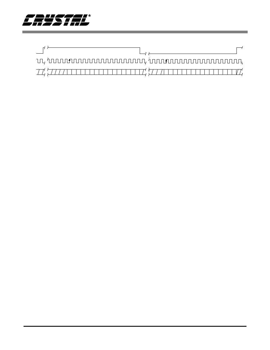
CS44210
36
DS539PP1
8. PARAMETER DEFINITIONS
Total Harmonic Distortion + Noise (THD+N)
The ratio of the rms value of the signal to the rms sum of all other spectral components over the specified
bandwidth (typically 10 Hz to 20 kHz), including distortion components. Expressed in decibels.
Dynamic Range
The ratio of the full scale rms value of the signal to the rms sum of all other spectral components over the
specified bandwidth. Dynamic range is a signal-to-noise measurement over the specified bandwidth
made with a -60 dBFS signal. 60 dB is then added to the resulting measurement to refer the measurement
to full scale. This technique ensures that the distortion components are below the noise level and do not
effect the measurement. This measurement technique has been accepted by the Audio Engineering So-
ciety, AES17-1991, and the Electronic Industries Association of Japan, EIAJ CP-307.
Interchannel Isolation
A measure of crosstalk between the left and right channels. Measured for each channel at the converter's
output with all zeros to the input under test and a full-scale signal applied to the other channel. Units in
decibels.
Interchannel Gain Mismatch
The gain difference between left and right channels. Units in decibels.
9.0 REFERENCES
1) "The I
2
C-Bus Specification: Version 2.0" Philips Semiconductors, December 1998.
http://www.semiconductors.philips.com
Figure 22. Right Justified, 16-Bit Data
LRCK
SCLK
Left Channel
Right Channel
SDATA
6
5
4
3
2
1
0
9
8
7
15 14 13 12 11 10
6
5
4
3
2
1
0
9
8
7
15 14 13 12 11 10
32 clocks
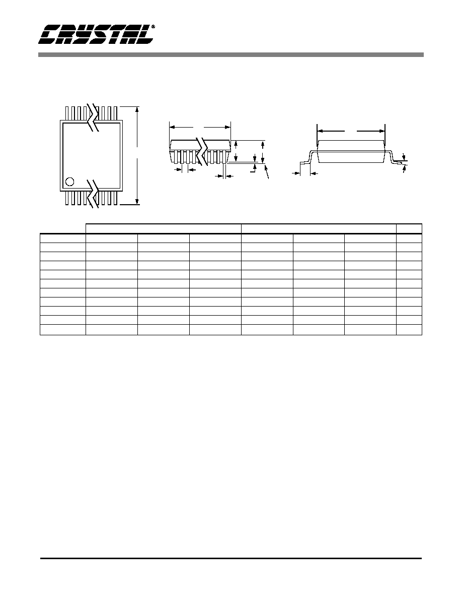
CS44210
DS539PP1
37
10. PACKAGE DIMENSIONS
Note:
1."D" and "E1" are reference datums and do not included mold flash or protrusions, but do include mold
mismatch and are measured at the parting line, mold flash or protrusions shall not exceed 0.20 mm per
side.
2.Dimension "b" does not include dambar protrusion/intrusion. Allowable dambar protrusion shall be
0.13 mm total in excess of "b" dimension at maximum material condition. Dambar intrusion shall not
reduce dimension "b" by more than 0.07 mm at least material condition.
3.These dimensions apply to the flat section of the lead between 0.10 and 0.25 mm from lead tips.
INCHES
MILLIMETERS
NOTE
DIM
MIN
NOM
MAX
MIN
NOM
MAX
A
--
--
0.043
--
--
1.10
A1
0.002
0.004
0.006
0.05
--
0.15
A2
0.03346
0.0354
0.037
0.85
0.90
0.95
b
0.00748
0.0096
0.012
0.19
0.245
0.30
2,3
D
0.303
0.307
0.311
7.70
7.80
7.90
1
E
0.248
0.2519
0.256
6.30
6.40
6.50
E1
0.169
0.1732
0.177
4.30
4.40
4.50
1
e
--
0.026 BSC
--
--
0.65 BSC
--
L
0.020
0.024
0.028
0.50
0.60
0.70
0∞
4∞
8∞
0∞
4∞
8∞
JEDEC #: MO-153
Controlling Dimension is Millimeters.
24L TSSOP (4.4 mm BODY) PACKAGE DRAWING
E
N
1 2 3
e
b
2
A1
A2
A
D
SEATING
PLANE
E1
1
L
SIDE VIEW
END VIEW
TOP VIEW
