Document Outline
- 1. Characteristics and Specifications
- 2. Pin Descriptions
- 3. Typical Connection Diagrams
- 4. Applications
- 5. Power Supply, Grounding, and PCB layout
- 6. Register Quick Reference
- 7. Register Description
- 7.1 Memory Address Pointer (MAP)
- 7.2 CS44600 I.D. and Revision Register (address 01h) (Read Only)
- 7.3 Clock Configuration and Power Control (address 02h)
- 7.4 PWM Channel Power Down Control (address 03h)
- 7.5 Misc. Configuration (address 04h)
- 7.6 Ramp Configuration (address 05h)
- 7.7 Volume Control Configuration (address 06h)
- 7.8 Master Volume Control - Integer (address 07h)
- 7.9 Master Volume Control - Fraction (address 08h)
- 7.10 Channel XX Volume Control - Integer (addresses 09h - 0Eh)
- 7.11 Channel XX Volume Control1 - Fraction (address 11h)
- 7.12 Channel XX Volume Control2 - Fraction (address 12h)
- 7.13 Channel Mute (address 13h)
- 7.14 Channel Invert (address 14h)
- 7.15 Peak Limiter Control Register (address 15h)
- 7.16 Limiter Attack Rate (address 16h)
- 7.17 Limiter Release Rate (address 17h)
- 7.18 Chnl XX Load Compensation Filter - Coarse Adjust (addresses�18h,�1Ah,�1Ch,�1Eh,�20h,�22h)
- 7.19 Chnl XX Load Compensation Filter - Fine Adjust (addresses�19h,�1Bh,�1Dh,�1Fh,�21h,�23h)
- 7.20 Interrupt Mode Control (address 28h)
- 7.21 Interrupt Mask (address 29h)
- 7.22 Interrupt Status (address 2Ah) (Read Only)
- 7.23 Channel Over Flow Status (address 2Bh) (Read Only)
- 7.24 GPIO Pin In/Out (address 2Ch)
- 7.25 GPIO Pin Polarity/Type (address 2Dh)
- 7.26 GPIO Pin Level/Edge Trigger (address 2Eh)
- 7.27 GPIO Status Register (address 2Fh)
- 7.28 GPIO Interrupt Mask Register (address 30h)
- 7.29 PWM Configuration Register (address 31h)
- 7.30 PWM Minimum Pulse Width Register (address 32h)
- 7.31 PWMOUT Delay Register (address 33h)
- 7.32 PSR and Power Supply Configuration (address 34h)
- 7.33 Decimator Shift/Scale (addresses�35h,�36h,�37h)
- 7.34 Decimator Outd (addresses�3Bh,�3Ch,�3Dh)
- 8. Parameter Definitions
- 9. References
- 10. Package Dimensions
- 11. Thermal Characteristics�
- 12. Revision History
Copyright
©
Cirrus Logic, Inc. 2005
(All Rights Reserved)
http://www.cirrus.com
Preliminary Product Information
This document contains information for a new product.
Cirrus Logic reserves the right to modify this product without notice.
6
-Channel Digital Amplifier Controller
Features
> 100 dB Dynamic Range - System Level
< 0.03% THD+N @ 1 W - System Level
32 kHz to 192 kHz Sample Rates
Internal Oscillator Circuit Supports 24.576 MHz
to 54 MHz Crystals
Integrated Sample Rate Converter (SRC)
≠ Eliminates Clock Jitter Effects
≠ Input Sample Rate Independent Operation
Power Supply Rejection Realtime Feedback
Spread Spectrum Modulation - Reduces
Modulation Energy
PWM PopGuard
Ѓ
for Single-Ended Mode
Eliminates AM Frequency Interference
Programmable Load Compensation Filters
Support for up to 40 kHz Audio Bandwidth
Digital Volume Control with Soft Ramp
≠ +24 to -127 dB in 0.25 dB Steps
Per Channel Programmable Peak Detect and
Limiter
SPI and I≤C Host Control Interfaces
Separate 2.5 V to 5.0 V Serial Port and Host
Control Port Supplies
DAI
Serial
Port
XT
A
L
PWMOUTA1+
Power
Supply
Rejection
PWMOUTB1+
SPI/I
2
C Host
Control Port
SCL/CCLK
SDA/CDOUT
AD1/CDIN
AD0/CS
RST
INT
PSR_MCLK
PSR_SYNC
PSR_DATA
PWM
Backend
Control/
Status
GPIO4
GPIO5
GPIO0
GPIO1
GPIO2
XTO
XTI
PWMOUTA1-
PWMOUTB1-
PWMOUTA2+
PWMOUTB2+
PWMOUTA2-
PWMOUTB2-
PWMOUTA3+
PWMOUTB3+
PWMOUTA3-
PWMOUTB3-
MUTE
DAI_MCLK
DAI_SCLK
DAI_LRCK
DAI_SDIN1
DAI_SDIN2
DAI_SDIN3
Volume
/ Limiter
Multibit
Modulator
PWM
Conversion
PWM
Conversion
PWM
Conversion
Volume
/ Limiter
Multibit
Modulator
Volume
/ Limiter
Multibit
Modulator
PWM
Clock
Control
Auto Fs
Detect
SYS_CLK
GPIO3
GPIO6
PSR_EN
PSR_RESET
PS_SYNC
SRC
MAY '05
DS633PP1
CS44600

2
DS633PP1
CS44600
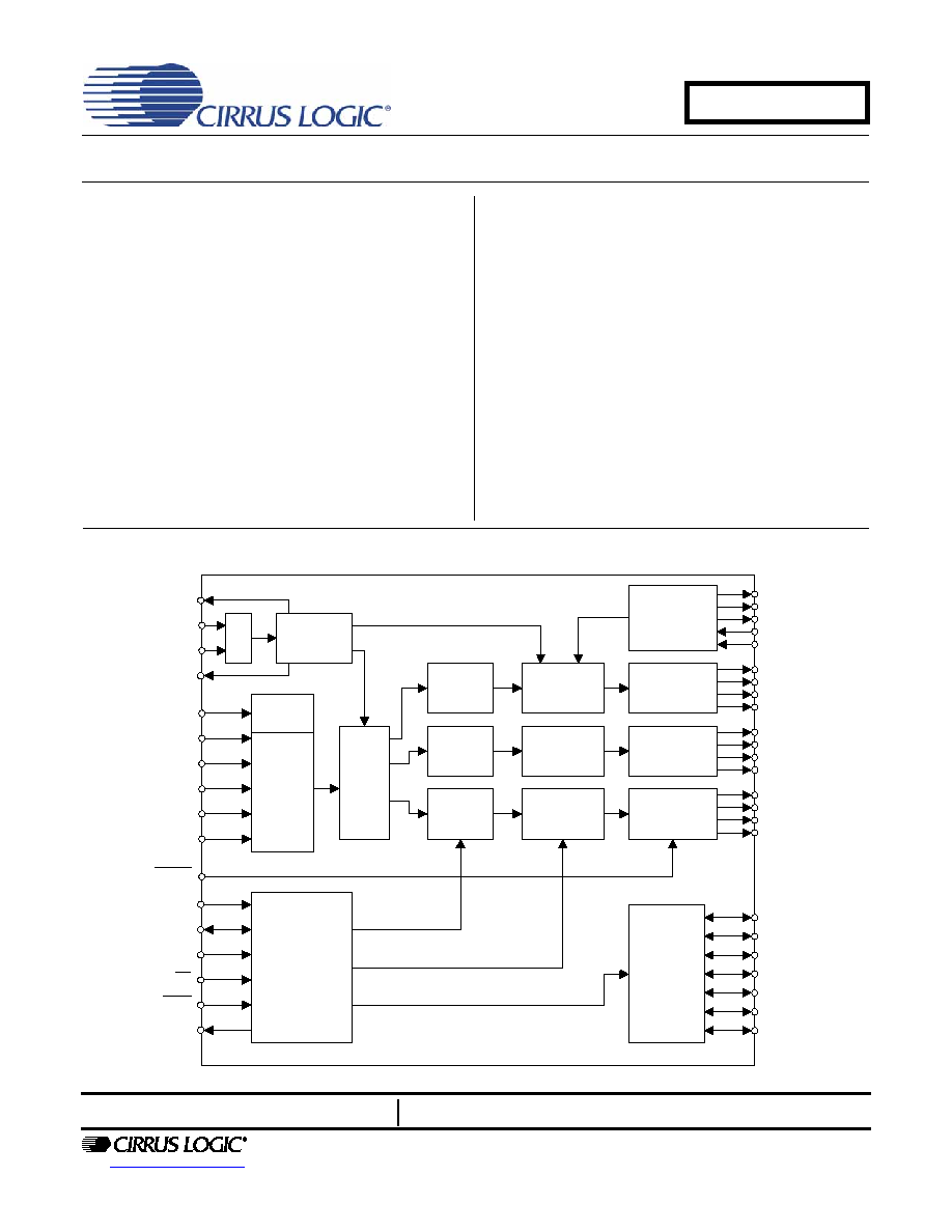
General Description
The CS44600 is a multi-channel digital-to-PWM Class D audio system controller including interpolation, sample rate
conversion, half- and full-bridge PWM driver outputs, and power supply rejection feedback in a 64-pin LQFP pack-
age.The architecture uses a direct-to-digital approach that maintains digital signal integrity to the final output filter,
minimizing analog interference effects which negatively affect system performance.
The CS44600 integrates on-chip digital volume control, peak detect with limiter, de-emphasis, and 7 GPIO's, allow-
ing easy interfacing to many commonly available power stages. The PWM amplifier can achieve greater than 90%
efficiency. This efficiency provides for smaller device package, less heat sink requirements, and smaller power
supplies.
The CS44600 is ideal for audio systems requiring wide dynamic range, negligible distortion and low noise, such as
A/V receivers, DVD receivers, digital speaker and automotive audio systems.
ORDERING INFORMATION
Product
Description
Package
Pb-Free
Temp Range Container
Order#
CS44600
6
-Channel Digital Amplifier
Controller
LQFP
YES
-10∞ to +70∞C
Rail
CS44600-CQZ
CS44600
6
-Channel Digital Amplifier
Controller
LQFP
YES
-10∞ to +70∞C
Tape and
Reel
CS44600-CQZR
CS44600
6
-Channel Digital Amplifier
Controller
LQFP
YES
-40∞ to +85∞C
Rail
CS44600-DQZ
CS44600
6
-Channel Digital Amplifier
Controller
LQFP
YES
-40∞ to +85∞C
Tape and
Reel
CS44600-DQZR
CDB44800
CS44600/800 Evaluation
Board
-
-
-
-
CDB44800
CRD44800
8x50 W Half-Bridge
Reference Design Board
-
-
-
-
CRD44800
CRD44800-ST-FB
8x60 W Full-Bridge
Reference Design Board
-
-
-
-
CRD44800-ST-FB
CRD44600-PH-FB
2x100 W Full-Bridge
Reference Design Board
-
-
-
-
CRD44600-PH-FB

DS633PP1
3
CS44600
TABLE OF CONTENTS
1. CHARACTERISTICS AND SPECIFICATIONS ........................................................................ 8
SPECIFIED OPERATING CONDITIONS ...................................................................................... 8
ABSOLUTE MAXIMUM RATINGS ................................................................................................. 8
DC ELECTRICAL CHARACTERISTICS ........................................................................................ 9
DIGITAL INTERFACE CHARACTERISTICS ................................................................................. 9
PWM OUTPUT PERFORMANCE CHARACTERISTICS ............................................................. 10
PWM FILTER CHARACTERISTICS ............................................................................................ 11
SWITCHING CHARACTERISTICS - XTI ..................................................................................... 11
SWITCHING CHARACTERISTICS - SYS_CLK .......................................................................... 12
SWITCHING CHARACTERISTICS - PWMOUTA1-B3 ................................................................ 12
SWITCHING CHARACTERISTICS - PS_SYNC .......................................................................... 12
SWITCHING CHARACTERISTICS - DAI INTERFACE ............................................................... 13
SWITCHING CHARACTERISTICS - CONTROL PORT - I≤C FORMAT ...................................... 14
SWITCHING CHARACTERISTICS - CONTROL PORT - SPI FORMAT ..................................... 15
2. PIN DESCRIPTIONS .............................................................................................................. 16
2.1 I/O Pin Characteristics ..................................................................................................... 19
3. TYPICAL CONNECTION DIAGRAMS ................................................................................... 20
4. APPLICATIONS ..................................................................................................................... 22
4.1 Overview .......................................................................................................................... 22
4.2 Feature Set Summary ..................................................................................................... 22
4.3 Clock Generation ............................................................................................................. 23
4.3.1 FsIn Domain Clocking ......................................................................................... 24
4.3.2 FsOut Domain Clocking ...................................................................................... 24
4.4 FsIn Clock Domain Modules ............................................................................................ 26
4.4.1 Digital Audio Input Port ....................................................................................... 26
4.4.2 Auto Rate Detect ................................................................................................. 30
4.4.3 De-Emphasis ...................................................................................................... 30
4.5 FsOut Clock Domain Modules ......................................................................................... 31
4.5.1 Sample Rate Converter ...................................................................................... 31
4.5.2 Load Compensation Filter ................................................................................... 31
4.5.3 Digital Volume and Mute Control ........................................................................ 31
4.5.4 Peak Detect / Limiter ........................................................................................... 32
4.5.5 PWM Engines ..................................................................................................... 32
4.5.6 Interpolation Filter ............................................................................................... 33
4.5.7 Quantizer ............................................................................................................ 33
4.5.8 Modulator ............................................................................................................ 33
4.5.9 PWM Outputs ...................................................................................................... 33
4.5.10 Power Supply Rejection (PSR) Real-Time Feedback ....................................... 34
4.6 Control Port Description and Timing ................................................................................ 35
4.6.1 SPI Mode ............................................................................................................ 35
4.6.2 I≤C Mode ............................................................................................................. 36
4.6.3 GPIOs ................................................................................................................. 37
4.6.4 Host Interrupt ...................................................................................................... 37
5. POWER SUPPLY, GROUNDING, AND PCB LAYOUT ......................................................... 38
5.1 Reset and Power-Up ....................................................................................................... 41
5.1.1 PWM PopGuardЃ Transient Control ................................................................... 41
5.1.2 Recommended Power-Up Sequence ................................................................. 41
5.1.3 Recommended PSR Calibration Sequence ....................................................... 42
5.1.4 Recommended Power-Down Sequence ............................................................. 43
6. REGISTER QUICK REFERENCE .......................................................................................... 44
7. REGISTER DESCRIPTION .................................................................................................... 48
7.1 Memory Address Pointer (MAP) ...................................................................................... 48

4
DS633PP1
CS44600
7.1.1 Increment (INCR) ................................................................................................ 48
7.1.2 Memory Address Pointer (MAPx) ....................................................................... 48
7.2 CS44600 I.D. and Revision Register (address 01h) (Read Only) ................................... 48
7.2.1 Chip I.D. (Chip_IDx) ............................................................................................ 48
7.2.2 Chip Revision (Rev_IDx) ..................................................................................... 48
7.3 Clock Configuration and Power Control (address 02h) ................................................... 49
7.3.1 Enable SYS_CLK Output (EN_SYS_CLK) ......................................................... 49
7.3.2 SYS_CLK Clock Divider Settings (SYS_CLK_DIV[1:0]) ..................................... 49
7.3.3 PWM Master Clock Divider Settings (PWM_MCLK_DIV[1:0]) ............................ 49
7.3.4 Power Down XTAL (PDN_XTAL) ........................................................................ 49
7.3.5 Power Down Output Mode (PDN_OUTPUT_MODE) ......................................... 50
7.3.6 Power Down (PDN) ............................................................................................. 50
7.4 PWM Channel Power Down Control (address 03h) ........................................................ 50
7.4.1 Power Down PWM Channels (PDN_PWMB3:PDN_PWMA1) ............................ 50
7.5 Misc. Configuration (address 04h) ................................................................................... 51
7.5.1 Digital Interface Format (DIFX) ........................................................................... 51
7.5.2 AM Frequency Hopping (AM_FREQ_HOP) ........................................................ 51
7.5.3 Freeze Controls (FREEZE) ................................................................................. 51
7.5.4 De-Emphasis Control (DEM[1:0]) ....................................................................... 52
7.6 Ramp Configuration (address 05h) ................................................................................. 52
7.6.1 Ramp-Up/Down Setting (RAMP[1:0]) ................................................................ 52
7.6.2 Ramp Speed (RAMP_SPD[1:0]) ......................................................................... 52
7.7 Volume Control Configuration (address 06h) .................................................................. 53
7.7.1 Single Volume Control (SNGVOL) ...................................................................... 53
7.7.2 Soft Ramp and Zero Cross Control (SZC[1:0]) ................................................... 53
7.7.3 Enable 50% Duty Cycle for Mute Condition (MUTE_50/50) ............................... 53
7.7.4 Soft Ramp-Down on Interface Error (SRD_ERR) .............................................. 54
7.7.5 Soft Ramp-Up on Recovered Interface Error (SRU_ERR) ................................. 54
7.7.6 Auto-Mute (AMUTE) ........................................................................................... 54
7.8 Master Volume Control - Integer (address 07h) .............................................................. 55
7.8.1 Master Volume Control - Integer (MSTR_IVOL[7:0]) .......................................... 55
7.9 Master Volume Control - Fraction (address 08h) ............................................................. 55
7.9.1 Master Volume Control - Fraction (MSTR_FVOL[1:0]) ....................................... 55
7.10 Channel XX Volume Control - Integer (addresses 09h - 0Eh) ....................................... 57
7.10.1 Channel Volume Control - Integer (CHXx_IVOL[7:0]) ...................................... 57
7.11 Channel XX Volume Control1 - Fraction (address 11h) .............................................. 57
7.12 Channel XX Volume Control2 - Fraction (address 12h) ................................................ 57
7.12.1 Channel Volume Control - Fraction (CHXX_FVOL[1:0]) ................................... 57
7.13 Channel Mute (address 13h) ......................................................................................... 58
7.13.1 Independent Channel Mute (CHXX_MUTE) ..................................................... 58
7.14 Channel Invert (address 14h) ........................................................................................ 58
7.14.1 Invert Signal Polarity (CHXX_INV) .................................................................... 58
7.15 Peak Limiter Control Register (address 15h) ............................................................... 59
7.15.1 Peak Signal Limit All Channels (LIMIT_ALL) .................................................... 59
7.15.2 Peak Signal Limiter Enable (LIMIT_EN) ........................................................... 59
7.16 Limiter Attack Rate (address 16h) ................................................................................ 59
7.16.1 Attack Rate (ARATE[7:0]) ................................................................................. 59
7.17 Limiter Release Rate (address 17h) ........................................................................... 60
7.17.1 Release Rate (RRATE[7:0]) .............................................................................. 60
7.18 Chnl XX Load Compensation Filter - Coarse Adjust (addresses 18h, 1Ah, 1Ch, 1Eh, 20h, 22h)
...................................................................................................................................... 60
7.18.1 Channel Compensation Filter - Coarse Adjust (CHXX_CORS[5:0]) ................. 60
7.19 Chnl XX Load Compensation Filter - Fine Adjust (addresses 19h, 1Bh, 1Dh, 1Fh, 21h, 23h)
...................................................................................................................................... 61

DS633PP1
5
CS44600
7.19.1 Channel Compensation Filter - Fine Adjust (CHXX_FINE[5:0]) ........................ 61
7.20 Interrupt Mode Control (address 28h) ........................................................................... 61
7.20.1 Interrupt Pin Control (INT1/INT0) ...................................................................... 61
7.20.2 Overflow Level/Edge Select (OVFL_L/E) .......................................................... 62
7.21 Interrupt Mask (address 29h) ........................................................................................ 62
7.22 Interrupt Status (address 2Ah) (Read Only) ................................................................. 62
7.22.1 SRC Unlock Interrupt (SRC_UNLOCK) ............................................................ 62
7.22.2 SRC Lock Interrupt (SRC_LOCK) ..................................................................... 63
7.22.3 Ramp-Up Complete Interrupt (RMPUP_DONE) ............................................... 63
7.22.4 Ramp-Down Complete Interrupt (RMPDN_DONE) .......................................... 63
7.22.5 Mute Complete Interrupt (Mute_DONE) ........................................................... 63
7.22.6 Channel Over Flow Interrupt (OVFL_INT) ........................................................ 63
7.22.7 GPIO Interrupt Condition (GPIO_INT) .............................................................. 63
7.23 Channel Over Flow Status (address 2Bh) (Read Only) ................................................. 64
7.23.1 ChXX_OVFL ..................................................................................................... 64
7.24 GPIO Pin In/Out (address 2Ch) ..................................................................................... 64
7.24.1 GPIO In/Out Selection (GPIOX_I/O) ................................................................. 64
7.25 GPIO Pin Polarity/Type (address 2Dh) .......................................................................... 64
7.25.1 GPIO Polarity/Type Selection (GPIOX_P/T) ..................................................... 64
7.26 GPIO Pin Level/Edge Trigger (address 2Eh) ................................................................. 65
7.26.1 GPIO Level/Edge Input Sensitive (GPIOX_L/E) ............................................... 65
7.27 GPIO Status Register (address 2Fh) ............................................................................. 65
7.27.1 GPIO Pin Status (GPIOX_STATUS) ................................................................. 65
7.28 GPIO Interrupt Mask Register (address 30h) ................................................................ 66
7.28.1 GPIO Pin Interrupt Mask (M_GPIOX) ............................................................... 66
7.29 PWM Configuration Register (address 31h) ................................................................. 66
7.29.1 Over Sample Rate Selection (OSRATE) .......................................................... 66
7.29.2 Channels A1 and B1 Output Configuration (A1/B1_OUT_CNFG) .................... 66
7.29.3 Channels A2 and B2 Output Configuration (A2/B2_OUT_CNFG) .................... 66
7.29.4 Channel A3 Output Configuration (A3_OUT_CNFG) ....................................... 67
7.29.5 Channel B3 Output Configuration (B3_OUT_CNFG) ....................................... 67
7.30 PWM Minimum Pulse Width Register (address 32h) .................................................... 67
7.30.1 Disable PWMOUTXX - Signal (DISABLE_PWMOUTXX-) ................................ 67
7.30.2 Minimum PWM Output Pulse Settings (MIN_PULSE[4:0]) ............................... 67
7.31 PWMOUT Delay Register (address 33h) ...................................................................... 68
7.31.1 Differential Signal Delay (DIFF_DLY[2:0]) ........................................................ 68
7.31.2 Channel Delay Settings (CHNL_DLY[4:0]) ...................................................... 68
7.32 PSR and Power Supply Configuration (address 34h) .................................................... 69
7.32.1 Power Supply Rejection Enable (PSR_EN) ...................................................... 69
7.32.2 Power Supply Rejection Reset (PSR_RESET) ................................................. 70
7.32.3 Power Supply Rejection Feedback Enable (FEEDBACK_EN) ......................... 70
7.32.4 Power Supply Sync Clock Divider Settings (PS_SYNC_DIV[2:0]) ................... 70
7.33 Decimator Shift/Scale (addresses 35h, 36h, 37h) ......................................................... 70
7.33.1 Decimator Shift (DEC_SHIFT[2:0]) ................................................................... 70
7.33.2 Decimator Scale (DEC_SCALE[18:0]) .............................................................. 71
7.34 Decimator Outd (addresses 3Bh, 3Ch, 3Dh) ................................................................. 71
7.34.1 Decimator Outd (DEC_OUTD[23:0]) ................................................................. 71
8. PARAMETER DEFINITIONS .................................................................................................. 72
9. REFERENCES ........................................................................................................................ 74
10. PACKAGE DIMENSIONS ........................................................................................... 75
11. THERMAL CHARACTERISTICS ......................................................................................... 76
12. REVISION HISTORY ............................................................................................................ 77